

Page 1
LM613
Dual Operational Amplifiers, Dual Comparators, and
Adjustable Reference
LM613 Dual Operational Amplifiers, Dual Comparators, and Adjustable Reference
August 2000
General Description
The LM613 consists of dual op-amps, dual comparators, and
a programmable voltage reference in a 16-pin package. The
op-amps out-performs most single-supply op-amps by providing higher speed and bandwidth along with low supply
current. This device was specifically designed to lower cost
and board space requirements in transducer, test, measurement, and data acquisition systems.
Combining a stable voltage reference with wide output swing
op-amps makes the LM613 ideal for single supply transducers, signal conditioning and bridge driving where large
common-mode-signals are common. The voltage reference
consists of a reliable band-gap design that maintains low dynamic output impedance (1Ω typical), excellent initial tolerance (0.6%), and the ability to be programmed from 1.2V to
6.3V via two external resistors. The voltage reference is very
stable even when driving large capacitive loads, as are commonly encountered in CMOS data acquisition systems.
As a member of National’s Super-Block
is a space-saving monolithic alternative to a multi-chip solution, offering a high level of integration without sacrificing
performance.
™
family, the LM613
Features
OP AMP
n Low operating current (Op Amp): 300 µA
n Wide supply voltage range: 4V to 36V
n Wide common-mode range: V
n Wide differential input voltage:
n Available in plastic package rated for Military Temp.
Range Operation
REFERENCE
n Adjustable output voltage: 1.2V to 6.3V
n Tight initial tolerance available:
n Wide operating current range: 17 µA to 20 mA
n Tolerant of load capacitance
−
to (V+− 1.8V)
±
36V
±
0.6%
Applications
n Transducer bridge driver
n Process and mass flow control systems
n Power supply voltage monitor
n Buffered voltage references for A/D’s
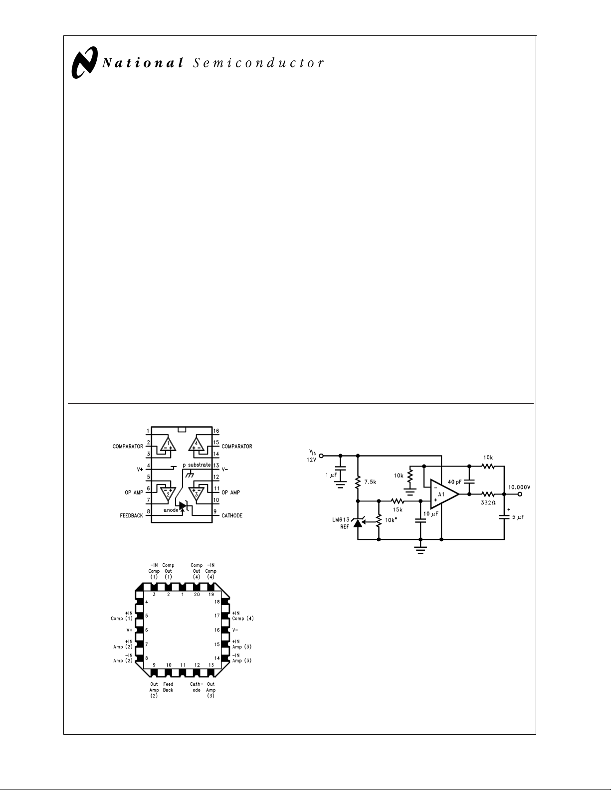
Ultra Low Noise, 10.00V Reference.
Total output noise is typically 14 µV
RMS
.
DS009226-1
Top View
E Package Pinout
*10k must be low
t.c. trimpot
DS009226-48
Super-Block™is a trademark of National Semiconductor Corporation.
© 2000 National Semiconductor Corporation DS009226 www.national.com
DS009226-43
Page 2
Absolute Maximum Ratings (Note 1)
LM613
If Military/Aerospace specified devices are required,
please contact the National Semiconductor Sales Office/
Distributors for availability and specifications.
Voltage on Any Pin Except V
(referred to V−pin)
(Note 2)
(Note 3)
Current through Any Input Pin
Pin
&V
R
Differential Input Voltage
Military and Industrial
Commercial
Storage Temperature Range −65˚C ≤ T
R
36V (Max)
−0.3V (Min)
±
20 mA
±
36V
±
32V
≤ +150˚C
J
Thermal Resistance,
Junction-to-Ambient (Note 5)
N Package
WM Package
Soldering Information (10 Sec.)
N Package
WM Package
ESD Tolerance (Note 6)
Operating Temperature Range
LM613AI, LM613BI: −40˚C to +85˚C
LM613AM, LM613M: −55˚C to +125˚C
LM613C: 0˚C ≤ T
Maximum Junction Temp.(Note 4) 150˚C
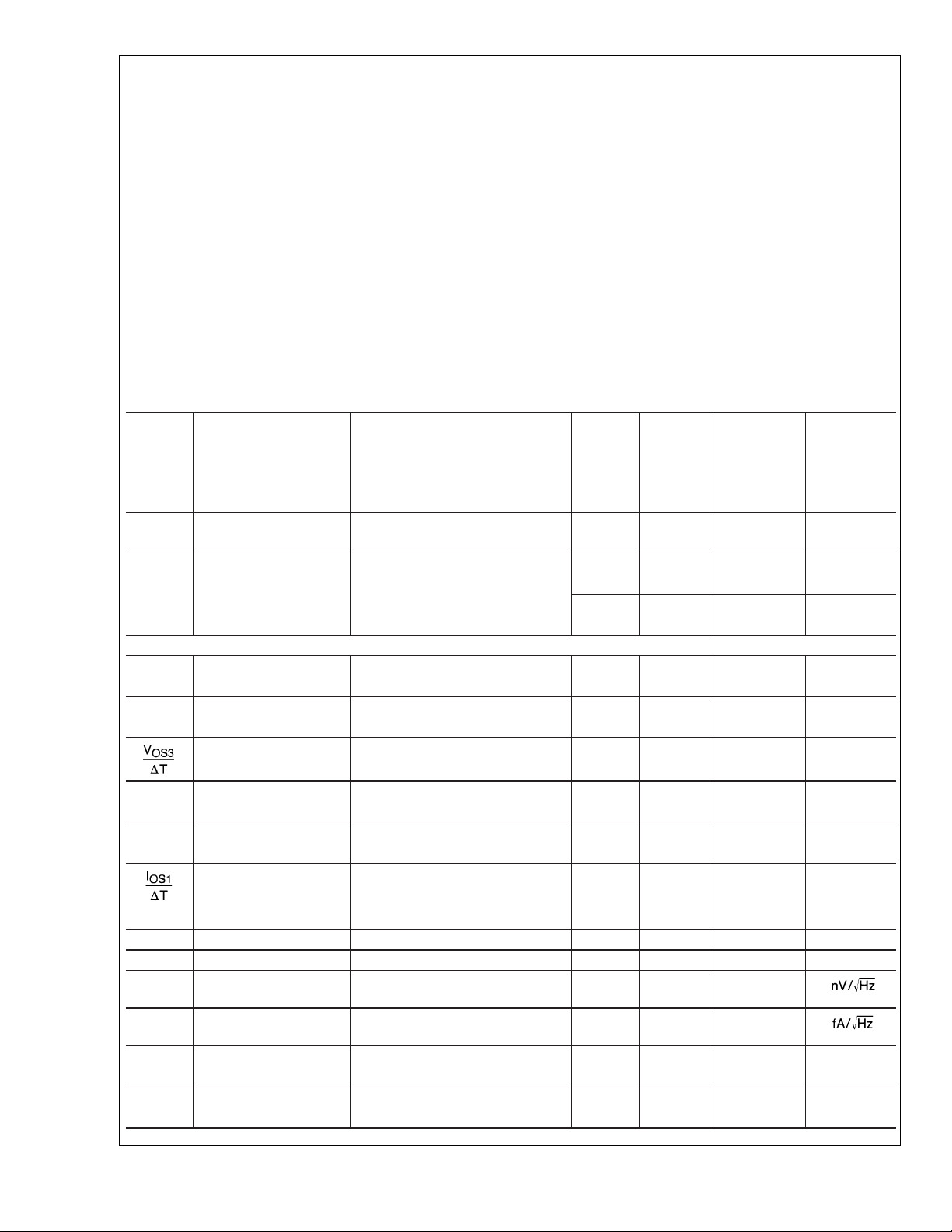
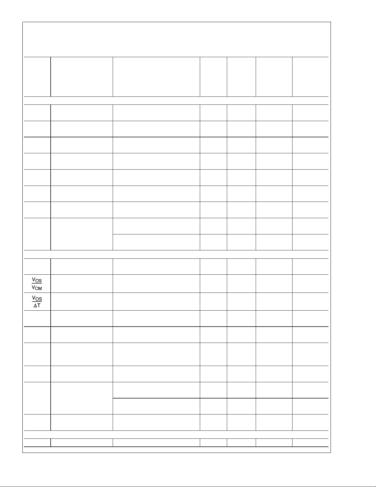
Electrical Characteristics
These specifications apply for V−= GND = 0V, V+= 5V, VCM=V
unless otherwise specified. Limits in standard typeface are for T
Temperature Range.
Symbol Parameter Conditions (Note 7) Limits LM613C Units
I
S
V
S
Total Supply Current R
Supply Voltage Range 2.2 2.8 2.8 V (Min)
=∞, 450 940 1000 µA (Max)
LOAD
+
4V ≤ V
≤ 36V (32V for LM613C) 550 1000 1070 µA (Max)
OPERATIONAL AMPLIFIERS
V
OS1
V
OS2
VOSOver Supply 4V ≤ V+≤ 36V 1.5 3.5 5.0 mV (Max)
+
VOSOver V
CM
(4V ≤ V
VCM= 0V through VCM= 1.0 3.5 5.0 mV (Max)
(V
≤ 32V for LM613C) 2.0 6.0 7.0 mV (Max)
+
− 1.8V), V+= 30V, V−=0V 1.5 6.0 7.0 mV (Max)
Average VOSDrift (Note 8) 15 µV/˚C
I
B
I
OS
Input Bias Current 10 25 35 nA (Max)
Input Offset Current 0.2 4 4 nA (Max)
Average Offset Current
= 2.5V, IR= 100 µA, FEEDBACK pin shorted to GND,
OUT
= 25˚C; limits in boldface type apply over the Operating
J
LM613AM LM613M
Typical LM613AI LM613I
(Note 8) Limits
(Note 8)
2.9 3 3 V (Min)
46 36 32 V (Max)
43 36 32 V (Max)
11 30 40 nA (Max)
0.3 5 5 nA (Max)
4 pA/˚C
100˚C/W
150˚C/W
260˚C
220˚C
±
1kV
≤ +70˚C
J
(Max)
R
IN
C
IN
e
n
I
n
Input Resistance Differential 1000 MΩ
Input Capacitance Common-Mode 6 pF
Voltage Noise f = 100 Hz, Input Referred 74
Current Noise f = 100 Hz, Input Referred 58
CMRR Common-Mode V+= 30V, 0V ≤ VCM≤ (V+− 1.8V) 95 80 75 dB (Min)
Rejection Ratio CMRR = 20 log (∆V
PSRR Power Supply 4V ≤ V
+
≤ 30V, VCM=V+/2, 110 80 75 dB (Min)
Rejection Ratio PSRR = 20 log (∆V
www.national.com 2
/∆VOS) 90 75 70 dB (Min)
CM
+
/VOS) 100 75 70 dB (Min)
Page 3
Electrical Characteristics (Continued)
These specifications apply for V−= GND = 0V, V+= 5V, VCM=V
unless otherwise specified. Limits in standard typeface are for TJ= 25˚C; limits in boldface type apply over the Operating
Temperature Range.
Symbol Parameter Conditions (Note 7) Limits LM613C Units
OPERATIONAL AMPLIFIERS
A
V
SR Slew Rate V
GBW Gain Bandwidth C
V
O1
V
O2
I
OUT
I
SINK
I
SHORT
Open Loop RL=10kΩto GND, V+= 30V, 500 100 94 V/mV
Voltage Gain 5V ≤ V
+
L
≤ 25V 50 40 40 (Min)
OUT
= 30V (Note 9) 0.70 0.55 0.50 V/µs
= 50 pF 0.8 MHz
Output Voltage RL=10kΩto GND, V+− 1.4 V+− 1.7 V+− 1.8 V (Min)
Swing High V
+
= 36V (32V for LM613C) V+− 1.6 V+− 1.9 V+− 1.9 V (Min)
Output Voltage RL=10kΩto V+,V
Swing Low V
Output Source Current V
Output Sink Current V
Short Circuit Current V
+
= 36V (32V for LM613C) V−+ 0.9 V−+ 1.0 V−+ 1.0 V (Max)
= 2.5V, V
OUT
−
V
= −0.3V 15 13 13 mA (Min)
IN
= 1.6V, V
OUT
−
V
= 0.3V 98 8mA (Min)
IN
= 0V,V
OUT
−
V
=2V 40 60 60 mA (Max)
IN
V
= 5V, V
OUT
−
V
=3V 32 80 90 mA (Max)
IN
+
= 0V, 25 20 16 mA (Min)
IN
+
= 0V, 17 14 13 mA (Min)
IN
+
= 3V, 30 50 50 mA (Max)
IN
+
= 2V, 30 60 70 mA (Max)
IN
COMPARATORS
V
OS
Offset Voltage 4V ≤ V+≤ 36V (32V for LM613C), 1.0 3.0 5.0 mV (Max)
R
=15kΩ 2.0 6.0 7.0 mV (Max)
L
Offset Voltage 0V ≤ VCM≤ 36V 1.0 3.0 5.0 mV (Max)
over V
CM
V+= 36V, (32V for LM613C) 1.5 6.0 7.0 mV (Max)
Average Offset 15 µV/˚C
Voltage Drift (Max)
I
B
I
OS
A
V
Input Bias Current 5 25 35 nA (Max)
Input Offset Current 0.2 4 4 nA (Max)
Voltage Gain RL=10kΩto 36V (32V for
LM613C)
t
r
I
SINK
I
LEAK
Large Signal V
Response Time R
Output Sink Current V
Output Leakage V
Current V
2V ≤ V
+
IN
L
+
IN
V
OUT
V
OUT
+
IN
OUT
≤ 27V 100 V/mV
OUT
= 1.4V, V
−
= TTL Swing, 1.5 µs
IN
= 5.1 kΩ 2.0 µs
−
= 0V, V
= 1V, 20 10 10 mA (Min)
IN
= 1.5V 13 8 8 mA (Min)
= 0.4V 2.8 1.0 0.8 mA (Min)
−
= 1V, V
= 0V, 0.1 10 10 µA (Max)
IN
= 36V (32V for LM613C) 0.2 µA (Max)
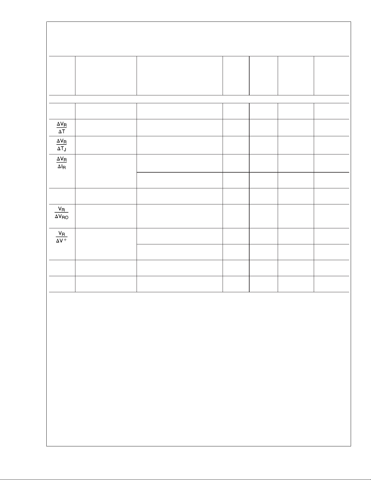
VOLTAGE REFERENCE
V
R
Voltage Reference (Note 10) 1.244 1.2365 1.2191 V (Min)
= 2.5V, IR= 100 µA, FEEDBACK pin shorted to GND,
OUT
LM613AM LM613M
Typical LM613AI LM613I
(Note 8) Limits
(Note 8)
0.65 0.45 0.45
0.5 MHz
−
+ 0.8 V−+ 0.9 V−+ 0.95 V (Max)
830 40nA (Max)
0.3 5 5 nA (Max)
500 V/mV
2.4 0.5 0.5 mA (Min)
LM613
www.national.com3
Page 4
Electrical Characteristics (Continued)
LM613
These specifications apply for V−= GND = 0V, V+= 5V, VCM=V
unless otherwise specified. Limits in standard typeface are for TJ= 25˚C; limits in boldface type apply over the Operating
Temperature Range.
Symbol Parameter Conditions (Note 7) Limits LM613C Units
VOLTAGE REFERENCE
Average Temp. Drift (Note 11) 10 80 150 ppm/˚C
Hysteresis (Note 12) 3.2 µV/˚C
= 2.5V, IR= 100 µA, FEEDBACK pin shorted to GND,
OUT
LM613AM LM613M
Typical LM613AI LM613I
(Note 8) Limits
(Note 8)
1.2515 1.2689 V (Max)
±
(
0.6%) (±2%)
(Max)
VRChange V
R(100 µA)−VR(17 µA)
0.05 1 1 mV (Max)
with Current 0.1 1.1 1.1 mV (Max)
V
R(10 mA)−VR(100 µA)
1.5 5 5 mV (Max)
(Note 13) 2.0 5.5 5.5 mV (Max)
R Resistance ∆V
∆V
VRChange V
with High V
RO
(5.06V between Anode and 2.8 10 10 mV (Max)
R(10→0.1 mA)
R(100→17 µA)
R(Vro = Vr)−VR(Vro = 6.3V)
/9.9 mA 0.2 0.56 0.56 Ω (Max)
/83 µA 0.6 13 13 Ω (Max)
2.5 7 7 mV (Max)
FEEDBACK)
VRChange with V
V
Change (V+= 32V for LM613C) 0.1 1.3 1.3 mV (Max)
ANODE
R(V+ = 5V)−VR(V+ = 36V)
V
R(V+ = 5V)−VR(V+ = 3V)
0.1 1.2 1.2 mV (Max)
0.01 1 1 mV (Max)
0.01 1.5 1.5 mV (Max)
I
FB
FEEDBACK Bias V
≤ VFB≤ 5.06V 22 35 50 nA (Max)
ANODE
Current 29 40 55 nA (Max)
e
n
Note 1: Absolute maximum ratings indicate limits beyond which damage to the component may occur. Electrical specifications do not apply when operating the device beyond its rated operating conditions.
Note 2: Input voltage above V
Note 3: More accurately, it is excessive current flow, with resulting excess heating, that limits the voltages on all pins. When any pin is pulled a diode drop below
−
V
, a parasitic NPN transistor turns ON. No latch-up will occur as long as the current through that pin remains below the Maximum Rating. Operation is undefined
and unpredictable when any parasitic diode or transistor is conducting.
Note 4: Simultaneous short-circuit of multiple comparators while using high supply voltages may force junction temperature above maximum, and thus should not
be continuous.
Note 5: Junction temperature may be calculated using T
soldered to copper-clad board with dissipation from one comparator or reference output transistor, nominal θ
WM package.
Note 6: Human body model, 100 pF discharged through a 1.5 kΩ resistor.
Note 7: Typical values in standard typeface are for T
most likely parametric norm.
Note 8: All limits are guaranteed at room temperature (standard type face) or at operating temperature extremes (bold type face).
Note 9: Slew rate is measured with the op amp in a voltage follower configuration. For rising slew rate, the input voltage is driven from 5V to 25V, and the output
voltage transition is sampled at 10V and
and 10V.
Note 10: V
Note 11: Average reference drift is calculated from the measurement of the reference voltage at 25˚C and at the temperature extremes. The drift, in ppm/˚C, is
6
10
is guaranteed by design and sample testing.
Note 12: Hysteresis is the change in V
hysteresis to the typical value, its junction temperature should be cycled in the following pattern, spiraling in toward 25˚C: 25˚C, 85˚C, −40˚C, 70˚C, 0˚C, 25˚C.
Note 13: Low contact resistance is required for accurate measurement.
VRNoise 10 Hz to 10 kHz, 30 µV
+
is allowed. As long as one input pin voltage remains inside the common-mode range, the comparator will deliver the correct output.
@
20V.For falling slew rate, the input voltage is driven from 25V to 5V,and the output voltage transition is sampled at 20V
is the Cathode-to-feedback voltage, nominally 1.244V.
R
∆VR/(V
•
∆TJ), where ∆VRis the lowest value subtracted from the highest, V
•
R[25˚C]
caused by a change in TJ, after the reference has been “dehysterized”. To dehysterize the reference; that is minimize the
R
VRO=V
R
J=TA+PDθJA
= 25˚C; values in bold face type apply for the full operating temperature range. These values represent the
J
. The given thermal resistance is worst-case for packages in sockets in still air. For packages
is the value at 25˚C, and ∆TJis the temperature range. This parameter
R[25˚C]
is 90˚C/W for the N package, and 135˚C/W for the
JA
RMS
www.national.com 4
Page 5
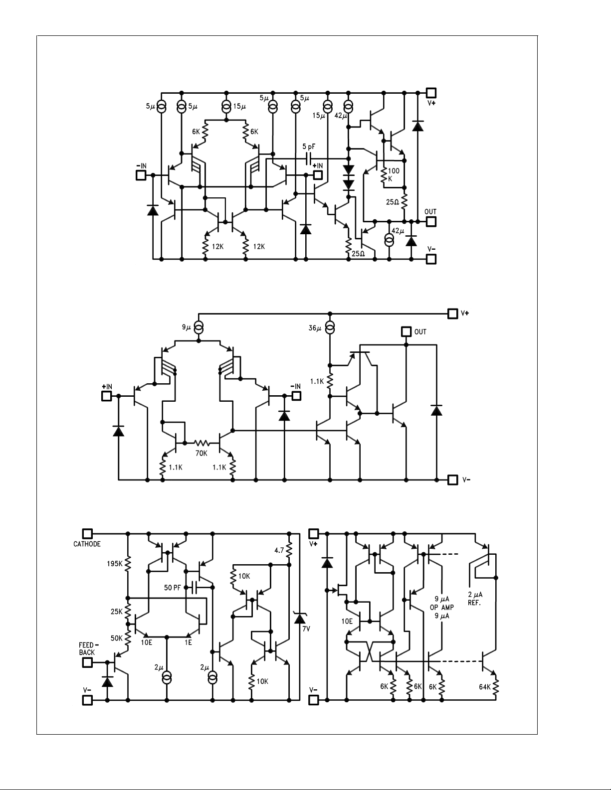
Simplified Schematic Diagrams
LM613
Op Amp
DS009226-2
Comparator
Reference/Bias
DS009226-3
DS009226-4
www.national.com5
Page 6
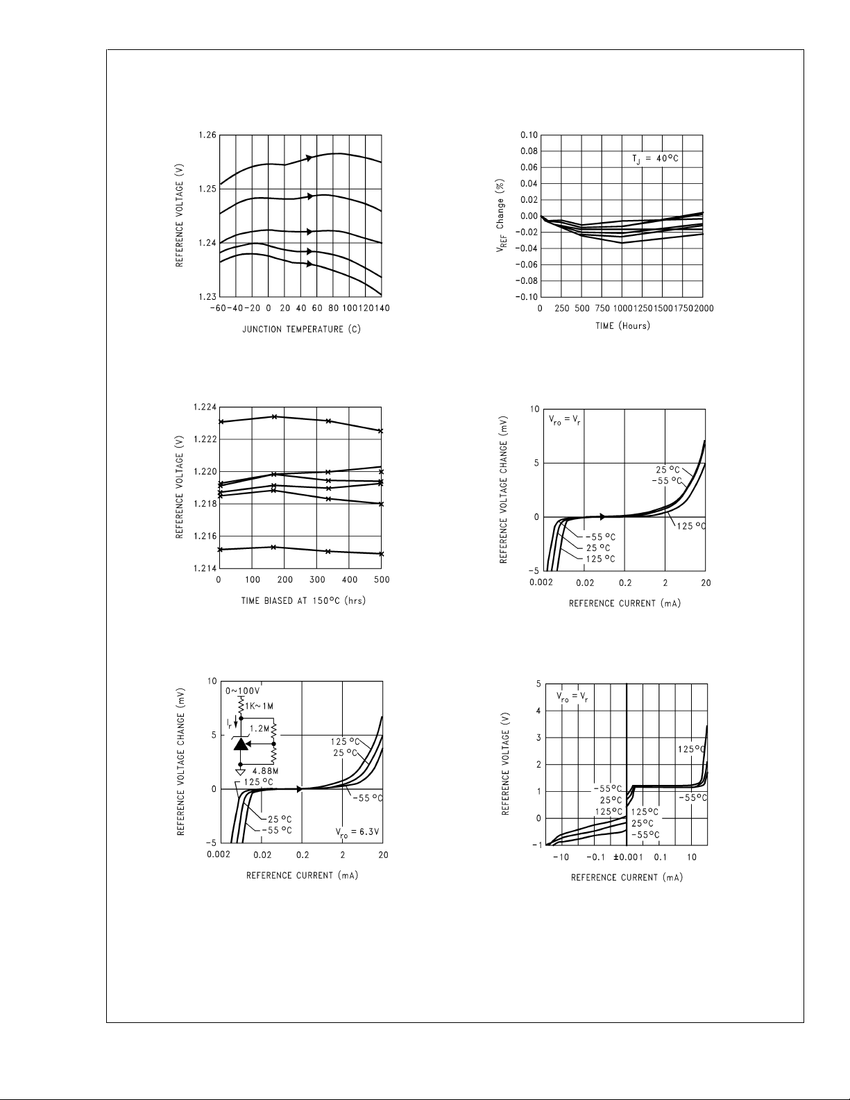
Typical Performance Characteristics (Reference) T
0V, unless otherwise noted
LM613
= 25˚C, FEEDBACK pin shorted to V−=
J
Reference Voltage vs Temp.
Accelerated Reference
Voltage Drift vs Time
DS009226-49
Reference Voltage Drift
DS009226-50
Reference Voltage vs
Current and Temperature
Reference Voltage vs
Current and Temperature
DS009226-51
DS009226-53
DS009226-52
Reference Voltage vs
Reference Current
DS009226-54
www.national.com 6
Page 7
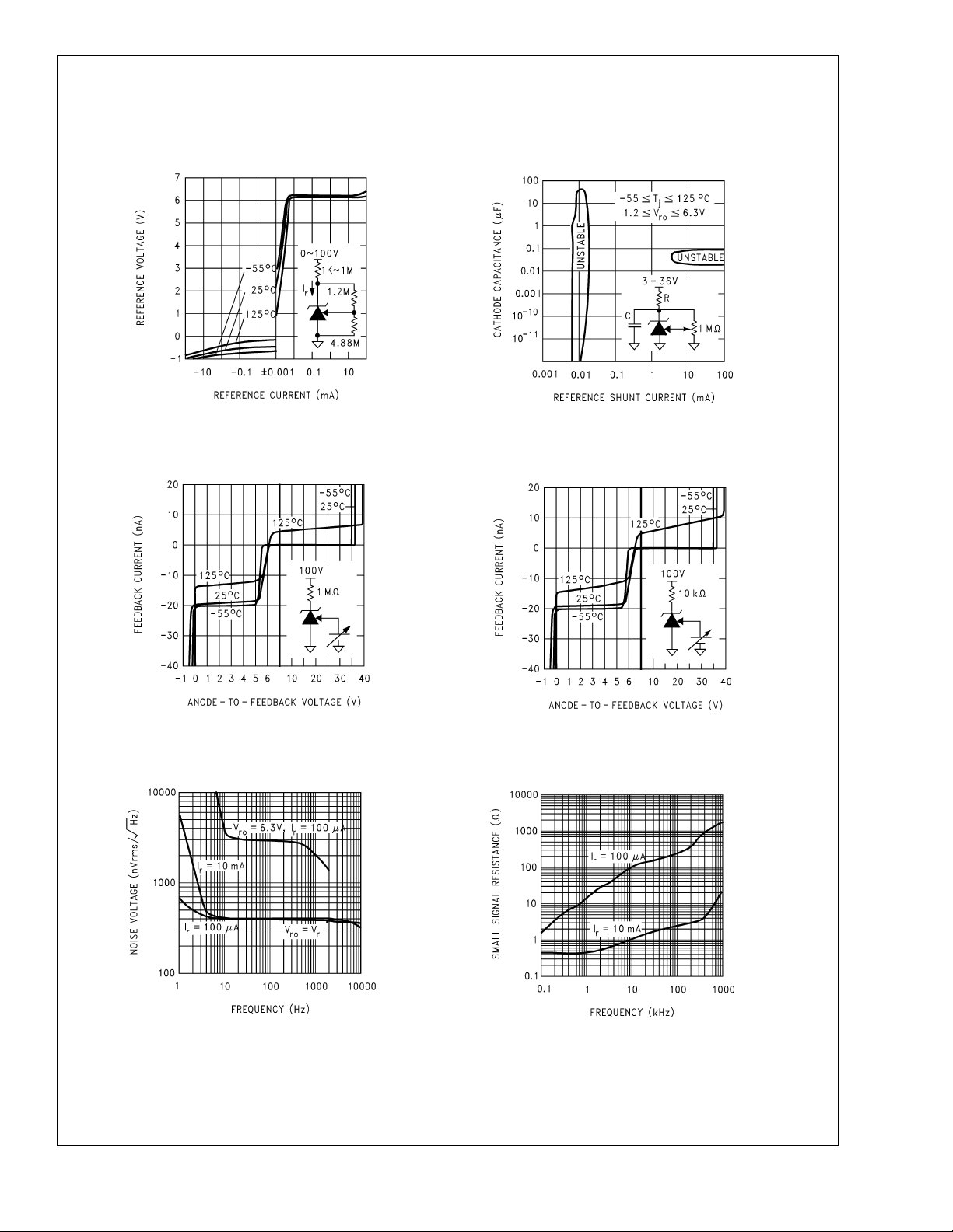
Typical Performance Characteristics (Reference) T
= 0V, unless otherwise noted (Continued)
= 25˚C, FEEDBACK pin shorted to V
J
LM613
−
Reference Voltage vs
Reference Current
FEEDBACK Current vs
FEEDBACK-to-Anode Voltage
DS009226-55
Reference AC
Stability Range
DS009226-56
FEEDBACK Current vs
FEEDBACK-to-Anode Voltage
Reference Noise Voltage
vs Frequency
DS009226-57
DS009226-59
DS009226-58
Reference Small-Signal
Resistance vs Frequency
DS009226-60
www.national.com7
Page 8

Typical Performance Characteristics (Reference) T
= 0V, unless otherwise noted (Continued)
LM613
= 25˚C, FEEDBACK pin shorted to V
J
−
Reference Power-Up Time
Reference Voltage with
100 ∼ 12 µA Current Step
Reference Voltage with
FEEDBACK Voltage Step
DS009226-61
DS009226-62
Reference Step Response
for 100 µA ∼ 10 mA
Current Step
Reference Voltage Change
with Supply Voltage Step
DS009226-63
DS009226-64
Reference Change vs
Common-Mode Voltage
DS009226-65
DS009226-66
www.national.com 8
Page 9

LM613
Typical Performance Characteristics (Op Amps) V
=V+/2, TJ= 25˚C, unless otherwise noted
Input Common-Mode
Voltage Range vs
Temperature
DS009226-67
Input Bias Current vs
Common-Mode Voltage
VOSvs Junction
Temperature
Large-Signal
Step Response
+
=5V,V−=GND=0V,VCM=V+/2, V
DS009226-68
OUT
Output Voltage Swing
vs Temp. and Current
DS009226-69
DS009226-71
DS009226-70
Output Source Current vs
Output Voltage and Temp.
DS009226-72
www.national.com9
Page 10

Typical Performance Characteristics (Op Amps) V
V
LM613
=V+/2, TJ= 25˚C, unless otherwise noted (Continued)
OUT
+
= 5V, V−= GND = 0V, VCM=V+/2,
Output Sink Current vs
Output Voltage
Output Impedance vs
Frequency and Gain
DS009226-73
Output Swing,
Large Signal
DS009226-74
Small Signal Pulse
Response vs Temp.
DS009226-75
Small-Signal Pulse
Response vs Load
DS009226-77
www.national.com 10
Op Amp Voltage Noise
vs Frequency
DS009226-76
DS009226-78
Page 11

Typical Performance Characteristics (Op Amps) V
V
=V+/2, TJ= 25˚C, unless otherwise noted (Continued)
OUT
+
= 5V, V−= GND = 0V, VCM=V+/2,
LM613
Op Amp Current Noise
vs Frequency
Small-Signal Voltage Gain
vs Frequency and Load
DS009226-79
Small-Signal Voltage Gain vs
Frequency and Temperature
DS009226-80
Follower Small-Signal
Frequency Response
Common-Mode Input
Voltage Rejection Ratio
DS009226-81
DS009226-83
DS009226-82
Power Supply Current
vs Power Supply Voltage
DS009226-84
www.national.com11
Page 12

Typical Performance Characteristics (Op Amps) V
V
LM613
=V+/2, TJ= 25˚C, unless otherwise noted (Continued)
OUT
+
= 5V, V−= GND = 0V, VCM=V+/2,
Positive Power Supply
Voltage Rejection Ratio
Slew Rate vs Temperature
DS009226-85
Negative Power Supply
Voltage Rejection Ratio
DS009226-86
Input Offset Current vs
Junction Temperature
Input Bias Current vs
Junction Temperature
DS009226-87
DS009226-88
DS009226-89
www.national.com 12
Page 13

Typical Performance Characteristics (Comparators)
LM613
Output Sink Current
Comparator
Response Times—Inverting
Input, Positive Transition
DS009226-10
Input Bias Current vs
Common-Mode Voltage
DS009226-11
Comparator
Response Times—Inverting
Input, Negative Transition
Comparator
Response Times—Non-Inverting
Input, Positive Transition
DS009226-12
DS009226-14
DS009226-13
Comparator
Response Times—Non-Inverting
Input, Negative Transition
DS009226-15
www.national.com13
Page 14

Typical Performance Characteristics (Comparators) (Continued)
LM613
Comparator
Response Times—Inverting
Input, Positive Transition
Comparator
Response Times—Inverting
Input, Negative Transition
DS009226-16
Comparator
Response Times—Non-Inverting
Input, Positive Transition
DS009226-18
Typical Performance Distributions
Average VOSDrift
Military Temperature Range
DS009226-17
Comparator
Response Times—Non-Inverting
Input, Negative Transition
DS009226-19
Average VOSDrift
Industrial Temperature Range
DS009226-20
www.national.com 14
DS009226-21
Page 15

Typical Performance Distributions (Continued)
LM613
Average V
Drift
OS
Commercial Temperature Range
DS009226-22
Average IOSDrift
Industrial Temperature Range
Average IOSDrift
Military Temperature Range
DS009226-23
Op Amp Voltage
Noise Distribution
DS009226-24
Average IOSDrift
Commercial Temperature Range
DS009226-25
DS009226-27
Op Amp Current
Noise Distribution
DS009226-28
www.national.com15
Page 16

Typical Performance Distributions
(Continued)
LM613
Voltage Reference Broad-Band
Noise Distribution
DS009226-26
Application Information
VOLTAGE REFERENCE
Reference Biasing
The voltage reference is of a shunt regulator topology that
models as a simple zener diode. With current I
“forward” direction there is the familiar diode transfer function. I
flowing in the reverse direction forces the reference
r
voltage to be developed from cathode to anode. The cathode may swing from a diode drop below V
voltage or to the avalanche voltage of the parallel protection
diode, nominally 7V. A 6.3V reference with V
allowed.
FIGURE 1. Voltage Associated with Reference
(current source I
is external)
r
−
to the reference
DS009226-29
flowing in the
r
+
=3Vis
DS009226-30
FIGURE 2. Reference Equivalent Circuit
DS009226-31
FIGURE 3. 1.2V Reference
Capacitors in parallel with the reference are allowed. See the
Reference AC Stability Range typical curve for capacitance
values—from 20 µA to 3 mA any capacitor value is stable.
With the reference’s wide stability range with resistive and
capacitive loads, a wide range of RC filter values will perform
noise filtering.
Adjustable Reference
The FEEDBACK pin allows the reference output voltage,
, to vary from 1.24V to 6.3V. The reference attempts to
V
ro
hold V
at 1.24V. If Vris above 1.24V, the reference will con-
r
duct current from Cathode to Anode; FEEDBACK current always remains low. If FEEDBACK is connected to Anode,
then V
= 1.24V. For higher voltages FEEDBACK is
ro=Vr
held at a constant voltage above Anode—say 3.76V for V
= 5V.Connecting a resistor across the constant Vrgenerates
a current I=R1/V
flowing from Cathode into FEEDBACK
r
node.A Thevenin equivalent 3.76V is generated from FEEDBACK to Anode with R2=3.76/I. Keep I greater than one
thousand times larger than FEEDBACK bias current for
<
0.1% error—I≥32 µAfor the military grade over the military
temperature range (I≥5.5 µA for a 1% untrimmed error for a
commercial part).
ro
The reference equivalent circuit reveals how V
is held at the
r
constant 1.2V by feedback, and how the FEEDBACK pin
passes little current.
To generate the required reverse current, typically a resistor
is connected from a supply voltage higher than the reference
voltage. Varying that voltage, and so varying I
, has small ef-
r
fect with the equivalent series resistance of less than an ohm
at the higher currents. Alternatively, an active current source,
such as the LM134 series, may generate I
www.national.com 16
.
r
DS009226-32
FIGURE 4. Thevenin Equivalent of Reference
with 5V Output
Page 17

Application Information (Continued)
LM613
DS009226-33
R1 = Vr/I = 1.24/32µ = 39k
R2 = R1 {(Vro/Vr) − 1} = 39k {(5/1.24) − 1)} = 118k
FIGURE 5. Resistors R1 and R2 Program Reference
Output Voltage to be 5V
Understanding that V
is fixed and that voltage sources, re-
r
sistors, and capacitors may be tied to the FEEDBACK pin, a
range of V
temperature coefficients may be synthesized.
r
DS009226-34
FIGURE 6. Output Voltage has Negative Temperature
Coefficient (TC) if R2 has Negative TC
DS009226-36
FIGURE 8. Diode in Series with R1 Causes Voltage
Across R1 and R2 to be Proportional to Absolute
Temperature (PTAT)
Connecting a resistor across Cathode-to-FEEDBACK creates a 0 TC current source, but a range of TCs may be
synthesized.
DS009226-37
I = Vr/R1 = 1.24/R1
FIGURE 9. Current Source is Programmed by R1
DS009226-35
FIGURE 7. Output Voltage has Positive TC
if R1 has Negative TC
DS009226-38
FIGURE 10. Proportional-to-Absolute-Temperature
Current Source
DS009226-39
FIGURE 11. Negative-TC Current Source
www.national.com17
Page 18

Application Information (Continued)
LM613
Reference Hysteresis
The reference voltage depends, slightly, on the thermal history of the die. Competitive micro-power products vary— always check the data sheet for any given device. Do not assume that no specification means no hysteresis.
OPERATIONAL AMPLIFIERS AND COMPARATORS
Any amp, comparator, or the reference may be biased in any
way with no effect on the other sections of the LM613, except when a substrate diode conducts, see Electrical Characteristics (Note 1). For example, one amp input may be outside the common-mode range, another amp may be
operating as a comparator, and all other sections may have
all terminals floating with no effect on the others. Tying inverting input to output and non-inverting input to V
used amps is preferred. Unused comparators should have
non-inverting input and output tied to V
tied to V
−
. Choosing operating points that cause oscillation,
such as driving too large a capacitive load, is best avoided.
Op Amp Output Stage
These op amps, like the LM124 series, have flexible and
relatively wide-swing output stages. There are simple rules
to optimize output swing, reduce cross-over distortion, and
optimize capacitive drive capability:
1. Output Swing: Unloaded, the 42 µA pull-down will bring
the output within 300 mV of V
ture range. If more than 42 µAis required, a resistor from
output to V
−
will help. Swing across any load may be improved slightly if the load can be tied to V
poorer sinking open-loop voltage gain.
2. Cross-Over Distortion: The LM613 has lower cross-over
distortion (a 1 V
deadband versus 3 VBEfor the
BE
+
, and inverting input
−
over the military tempera-
+
−
on un-
, at the cost of
LM124), and increased slew rate as shown in the characteristic curves.A resistor pull-up or pull-down will force
class-A operation with only the PNP or NPN output transistor conducting, eliminating cross-over distortion.
3. Capacitive Drive: Limited by the output pole caused by
the output resistance driving capacitive loads, a
pull-down resistor conducting 1 mA or more reduces the
output stage NPN r
until the output resistance is that of
e
the current limit 25Ω. 200 pF may then be driven without
oscillation.
Comparator Output Stage
The comparators, like the LM139 series, have open-collector
output stages. A pull-up resistor must be added from each
output pin to a positive voltage for the output transistor to
switch properly. When the output transistor is OFF, the output voltage will be this external positive voltage.
For the output voltage to be under the TTL-low voltage
threshold when the output transistor is ON, the output current must be less than 8 mA (over temperature). This impacts the minimum value of pull-up resistor.
The offset voltage may increase when the output voltage is
low and the output current is less than 30 µA. Thus, for best
accuracy, the pull-up resistor value should be low enough to
allow the output transistor to sink more than 30 µA.
Op Amp and Comparator Input Stage
The lateral PNP input transistors, unlike those of most op
amps, have BV
equal to the absolute maximum supply
EBO
voltage.Also, they have no diode clamps to the positive supply nor across the inputs. These features make the inputs
look like high impedances to input sources producing large
differential and common-mode voltages.
Typical Applications
DS009226-40
FIGURE 12. High Current, High Voltage Switch
www.national.com 18
Page 19

Typical Applications (Continued)
FIGURE 13. High Speed Level Shifter. Response time is approximately
1.5 µs, where output is either approximately +V or −V.
LM613
DS009226-41
*10k must be low
t.c. trimpot
DS009226-43
FIGURE 14. Ultra Low Noise, 10.00V Reference. Total output noise is typically 14 µV
RMS
.
www.national.com19
Page 20

Typical Applications (Continued)
LM613
FIGURE 15. Basic Comparator
FIGURE 16. Basic Comparator with External Strobe
Ordering Information
DS009226-44
DS009226-45
FIGURE 17. Wide-Input Range
Comparator with TTL Output
DS009226-47
FIGURE 18. Comparator with
Hysteresis (∆V
=+V(1k/1M))
H
DS009226-46
Reference
Tolerance & V
±
0.6%
OS
−55˚C ≤ T
LM613AMJ/883 (Note 14) 16-Pin
80 ppm/˚C Max.
≤ 3.5 mV
V
OS
±
2.0%
150 ppm/˚C Max.
≤ 5.0 mV Max.
V
OS
Note 14: A military RETS 613AMX electrical test specification is available on request. The Military screened parts can also be procured as a Standard Military Drawing.
Temperature Range
Military Industrial
≤ +125˚C −40˚C ≤ TA≤ +85˚C
A
LM613IWM
LM613IWMX
Package
Ceramic DIP
16-Pin Wide
Surface Mount
NSC
Drawing
J16A
M16B
www.national.com 20
Page 21

Physical Dimensions inches (millimeters) unless otherwise noted
16-Lead Ceramic Dual-In-Line Package (J)
Order Number LM613AMJ/883
NS Package Number J16A
LM613
16-Lead Small Outline Package (WM)
Order Number LM613IWM or LM613IWMX
NS Package Number M16B
www.national.com21
Page 22

Notes
LIFE SUPPORT POLICY
NATIONAL’S PRODUCTS ARE NOT AUTHORIZED FOR USE AS CRITICAL COMPONENTS IN LIFE SUPPORT
DEVICES OR SYSTEMS WITHOUT THE EXPRESS WRITTEN APPROVAL OF THE PRESIDENT AND GENERAL
COUNSEL OF NATIONAL SEMICONDUCTOR CORPORATION. As used herein:
1. Life support devices or systems are devices or
systems which, (a) are intended for surgical implant
LM613 Dual Operational Amplifiers, Dual Comparators, and Adjustable Reference
into the body, or (b) support or sustain life, and
whose failure to perform when properly used in
accordance with instructions for use provided in the
2. A critical component is any component of a life
support device or system whose failure to perform
can be reasonably expected to cause the failure of
the life support device or system, or to affect its
safety or effectiveness.
labeling, can be reasonably expected to result in a
significant injury to the user.
National Semiconductor
Corporation
Americas
Tel: 1-800-272-9959
Fax: 1-800-737-7018
Email: support@nsc.com
www.national.com
National does not assume any responsibility for use of any circuitry described, no circuit patent licenses are implied and National reserves the right at any time without notice to change said circuitry and specifications.
National Semiconductor
Europe
Fax: +49 (0) 180-530 85 86
Email: europe.support@nsc.com
Deutsch Tel: +49 (0) 69 9508 6208
English Tel: +44 (0) 870 24 0 2171
Français Tel: +33 (0) 1 41 91 8790
National Semiconductor
Asia Pacific Customer
Response Group
Tel: 65-2544466
Fax: 65-2504466
Email: ap.support@nsc.com
National Semiconductor
Japan Ltd.
Tel: 81-3-5639-7560
Fax: 81-3-5639-7507
 Loading...