

Page 1
LM6132 Dual/LM6134 Quad
Low Power 10 MHz Rail-to-Rail I/O Operational
Amplifiers
LM6132 Dual and LM6134 Quad, Low Power 10 MHz Rail-to-Rail I/O Operational Amplifiers
April 2000
General Description
The LM6132/34 provides new levels of speed vs power performance in applications where low voltage supplies or
power limitations previously made compromise necessary.
With only 360 µA/amp supply current, the 10 MHz
gain-bandwidth ofthis device supports new portable applications where higher power devices unacceptably drain battery
life.
The LM6132/34 can be driven by voltages that exceed both
power supply rails, thus eliminating concerns over exceeding
the common-mode voltage range. The rail-to-rail output
swing capability provides the maximum possible dynamic
range at the output. This is particularly important when operating on low supply voltages. The LM6132/34 can also drive
large capacitive loads without oscillating.
Operating on supplies from 2.7V to over 24V,the LM6132/34
is excellent for a very wide range of applications, from battery operated systems with large bandwidth requirements to
high speed instrumentation.
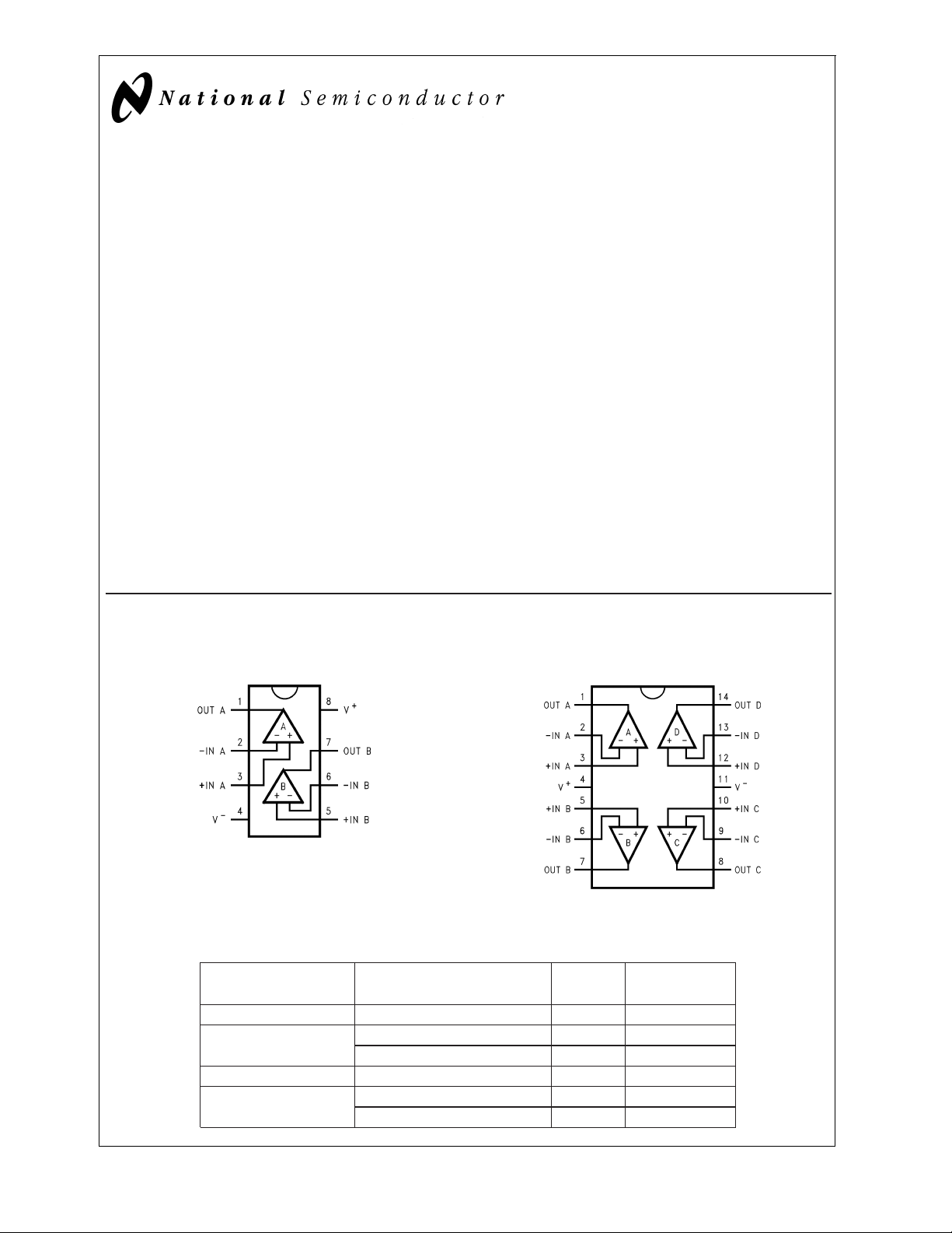
Connection Diagrams
8-Pin DIP/SO
Features
(For 5V Supply, Typ Unless Noted)
n Rail-to-Rail input CMVR −0.25V to 5.25V
n Rail-to-Rail output swing 0.01V to 4.99V
n High gain-bandwidth, 10 MHz at 20 kHz
n Slew rate 12 V/µs
n Low supply current 360 µA/Amp
n Wide supply range 2.7V to over 24V
n CMRR 100 dB
n Gain 100 dB with R
n PSRR 82 dB
L
= 10k
Applications
n Battery operated instrumentation
n Instrumentation Amplifiers
n Portable scanners
n Wireless communications
n Flat panel display driver
14-Pin DIP/SO
DS012349-1
Top View
DS012349-2
Top View
Ordering Information
Package Temperature Range NSC Transport
Industrial, −40˚C to +85˚C Drawing Media
8-Pin Molded DIP LM6132AIN, LM6132BIN N08E Rails
8-Pin Small Outline LM6132AIM, LM6132BIM M08A Rails
LM6132AIMX, LM6132BIMX M08A Tape and Reel
14-Pin Molded DIP LM6134AIN, LM6134BIN N14A Rails
14-Pin Small Outline LM6134AIM, LM6134BIM M14A Rails
LM6134AIMX, LM6134BIMX M14A Tape and Reel
© 2000 National Semiconductor Corporation DS012349 www.national.com
Page 2
Absolute Maximum Ratings (Note 1)
Junction Temperature (Note 4) 150˚C
If Military/Aerospace specified devices are required,
please contact the National Semiconductor Sales Office/
Distributors for availability and specifications.
ESD Tolerance (Note 2) 2500V
LM6132/LM6134
Differential Input Voltage 15V
Voltage at Input/Output Pin (V
+–V−
Supply Voltage (V
) 35V
+
)+0.3V, (V−)−0.3V
Current at Input Pin
Current at Output Pin (Note 3)
Current at Power Supply Pin 50 mA
±
10 mA
±
25 mA
Operating Ratings(Note 1)
Supply Voltage 1.8V ≤ V
Junction Temperature Range
LM6132, LM6134 −40˚C ≤ T
Thermal resistance (θ
N Package, 8-pin Molded DIP 115˚C/W
M Package, 8-pin Surface Mount 193˚C/W
N Package, 14-pin Molded DIP 81˚C/W
M Package, 14-pin Surface Mount 126˚C/W
)
JA
Lead Temp. (soldering, 10 sec.) 260˚C
Storage Temperature Range −65˚C to +150˚C
5.0V DC Electrical Characteristics
Unless otherwise specified, all limits guaranteed for TJ= 25˚C, V+= 5.0V, V−= 0V, VCM=VO=V+/2 and R
Boldface limits apply at the temperature extremes
LM6134AI LM6134BI
Symbol Parameter Conditions
V
OS
TCV
I
B
I
OS
R
IN
CMRR Common Mode Rejection Ratio 0V ≤ V
PSRR Power Supply Rejection Ratio
V
CM
Input Offset Voltage 0.25 2
Input Offset Voltage Average Drift 5 µV/C
OS
Input Bias Current 0V ≤ VCM≤ 5V 110 140
Input Offset Current 3.4 30
Input Resistance, CM 104 MΩ
≤ 4V 100 75
CM
0V ≤ V
±
2.5V ≤ VS≤±12V 82 78
≤ 5V 80 60
CM
Input Common-Mode Voltage
Range
A
V
V
O
Large Signal Voltage Gain RL= 10k 100 25
Output Swing 100k Load 4.992 4.98
10k Load 4.952 4.94
5k Load 4.923 4.90
I
SC
Output Short Circuit Current
Sourcing 4 2
LM6132
Sinking 3.5 1.8
Typ
(Note 5)
−0.25 00
5.25 5.0 5.0
0.007 0.017
0.032 0.07
0.051 0.095
LM6132AI LM6132BI
Limit Limit
(Note 6) (Note 6)
4
300
50
70
55
75
8
4.93
0.019
4.85
0.09
4.85
0.12
2
1.8
L
6
8
180
350
30
50
75
70
60
55
78
75
15
6
4.98
4.93
0.017
0.019
4.94
4.85
0.07
0.09
4.90
4.85
0.095
0.12
2
1
1.8
1
>
≤ 24V
S
≤ +85˚C
J
1MΩto VS/2.
Units
mV
max
nA
max
nA
max
dB
min
dB
min
V
V/mV
min
V
min
V
max
V
min
V
max
V
min
V
max
mA
min
mA
min
www.national.com 2
Page 3
5.0V DC Electrical Characteristics (Continued)
Unless otherwise specified, all limits guaranteed for TJ= 25˚C, V+= 5.0V, V−= 0V, VCM=VO=V+/2 and R
Boldface limits apply at the temperature extremes
LM6134AI LM6134BI
Symbol Parameter Conditions
Typ
(Note 5)
LM6132AI LM6132BI
Limit Limit
(Note 6) (Note 6)
I
SC
Output Short Circuit Current
LM6134
Sourcing 3 2
1.6
Sinking 3.5 1.8
1.3
I
S
Supply Current Per Amplifier
360
400
450
>
1MΩto VS/2.
L
2
1
1.8
1
400
450
Units
mA
min
mA
min
µA
max
5.0V AC Electrical Characteristics
Unless otherwise specified, all limits guaranteed for TJ= 25˚C, V+= 5.0V, V−= 0V, VCM=VO=V+/2 and R
Boldface limits apply at the temperature extremes
LM6134AI LM6134BI
Symbol Parameter Conditions
Typ
(Note 5)
LM6132AI LM6132BI
Limit Limit
(Note 6) (Note 6)
±
SR Slew Rate
4V@VS=±6V 14 8 8 V/µs
<
R
1kΩ 77min
S
GBW Gain-Bandwidth Product f = 20 kHz 10 7.4 7.4 MHz
77min
θm Phase Margin R
G
m
e
n
Gain Margin RL= 10k 10 dB
Input Referred Voltage Noise f = 1 kHz 27
= 10k 33 deg
L
>
1MΩto VS/2.
L
Units
LM6132/LM6134
i
n
Input Referred Current Noise f = 1 kHz 0.18
www.national.com3
Page 4
2.7V DC Electrical Characteristics
Unless otherwise specified, all limits guaranteed for TJ= 25˚C, V+= 2.7V, V−= 0V, VCM=VO=V+/2 and R
Boldface limits apply at the temperature extreme
LM6134AI LM6134BI
Symbol Parameter Conditions
LM6132/LM6134
V
OS
I
B
I
OS
R
IN
Input Offset Voltage 0.12 2 6 mV
Input Bias Current 0V ≤ VCM≤ 2.7V 90 nA
Input Offset Current 2.8 nA
Input Resistance 134 MΩ
CMRR Common Mode 0V ≤ V
Rejection Ratio
PSRR Power Supply
±
1.35V ≤ VS≤±12V 80 dB
Rejection Ratio
V
CM
Input Common-Mode 2.7 2.7 V
Voltage Range 0 0
A
V
Large Signal RL= 10k 100 V/mV
Voltage Gain
V
O
I
S
Output Swing RL= 100k 0.03 0.08 0.08 V
Supply Current Per Amplifier 330 µA
Typ
(Note 5)
≤ 2.7V 82 dB
CM
2.66 2.65 2.65 V
LM6132AI LM6132BI
Limit Limit
(Note 6) (Note 6)
812max
0.112 0.112 max
2.25 2.25 min
>
1MΩto VS/2.
L
Units
2.7V AC Electrical Characteristics
Unless otherwise specified, all limits guaranteed for TJ= 25˚C, V+= 2.7V, V−= 0V, VCM=VO=V+/2 and R
LM6134AI LM6134BI
Symbol Parameter Conditions
GBW Gain-Bandwidth Product R
θ
m
G
m
Phase Margin RL= 10k 23 deg
Gain Margin 12 dB
= 10k, f = 20 kHz 7 MHz
L
Typ
(Note 5)
LM6132AI LM6132BI
Limit Limit
(Note 6) (Note 6)
>
1MΩto VS/2.
L
Units
www.national.com 4
Page 5
24V DC Electrical Characteristics
Unless otherwise specified, all limits guaranteed for TJ= 25˚C, V+= 24V, V−= 0V, VCM=VO=V+/2 and R
Boldface limits apply at the temperature extreme
LM6134AI LM6134BI
Symbol Parameter Conditions
V
OS
I
B
I
OS
R
IN
CMRR Common Mode 0V ≤ V
Input Offset Voltage 1.7 3 7 mV
Input Bias Current 0V ≤ VCM≤ 24V 125 nA
Input Offset Current 4.8 nA
Input Resistance 210 MΩ
≤ 24V 80 dB
CM
Rejection Ratio
PSRR Power Supply 2.7V ≤ V
≤ 24V 82 dB
S
Rejection Ratio
V
CM
Input Common-Mode −0.25 0 0 V min
Voltage Range 24.25 24 24 V max
A
V
Large Signal RL= 10k 102 V/mV
Voltage Gain
V
O
I
S
Output Swing RL= 10k 0.075 0.15 0.15 V
Supply Current Per Amplifier 390 450 450 µA
Typ
(Note 5)
23.86 23.8 23.8 V
LM6132AI LM6132BI
Limit Limit
(Note 6) (Note 6)
59max
490 490 max
>
1MΩto VS/2.
L
LM6132/LM6134
Units
max
min
24V AC Electrical Characteristics
Unless otherwise specified, all limits guaranteed for TJ= 25˚C, V+= 24V, V−= 0V, VCM=VO=V+/2 and R
LM6134AI LM6134BI
Symbol Parameter Conditions
Typ
(Note 5)
LM6132AI LM6132BI
Limit Limit
(Note 6) (Note 6)
GBW Gain-Bandwidth Product R
θ
m
G
m
THD +
Phase Margin RL= 10k 23 deg
Gain Margin RL= 10k 12 dB
Total Harmonic A
N
= 10k, f = 20 kHz 11 MHz
L
= +1, VO= 20V
V
P-P
0.0015 %
Distortion and Noise f = 10 kHz
Note 1: Absolute Maximum Ratings indicate limits beyond which damage to the device may occur. Operating Ratings indicate conditions for which the device is intended to be functional, but specific performance is not guaranteed. For guaranteed specifications and the test conditions, see the Electrical characteristics.
Note 2: Human body model, 1.5 kΩ in series with 100 pF.
Note 3: Applies to both single-supply and split-supply operation. Continuous short circuit operation at elevated ambient temperature can result in exceeding the
maximum allowed junction temperature of 150˚C.
Note 4: The maximum power dissipation isafunctionofT
−TA)/θJA. All numbers apply for packages soldered directly into a PC board.
Note 5: Typical Values represent the most likely parametric norm.
Note 6: All limits are guaranteed by testing or statistical analysis.
, θJA, and TA. The maximum allowable power dissipation at any ambient temperature is PD=(T
J(max)
>
1MΩto VS/2.
L
Units
J(max)
www.national.com5
Page 6

Typical Performance Characteristics T
= 25˚C, RL=10kΩunless otherwise specified
A
Supply Current vs
Supply Voltage
LM6132/LM6134
dVOSvs V
CM
DS012349-3
Offset Voltage vs
Supply Voltage
dVOSvs V
CM
DS012349-5
dVOSvs V
I
vs V
bias
CM
DS012349-6
CM
I
vs V
bias
CM
Neg PSRR vs
Frequency
DS012349-7
DS012349-10
I
vs V
bias
CM
Pos PSSR vs
Frequency
DS012349-8
DS012349-11
DS012349-9
Input Bias Current vs
Supply Voltage
DS012349-12
dVOSvs
Output Voltage
DS012349-13
www.national.com 6
DS012349-14
DS012349-15
Page 7

LM6132/LM6134
Typical Performance Characteristics T
dV
vs
OS
Output Voltage
Output Voltage vs
Sinking Current
DS012349-16
dVOSvs
Output Voltage
Output Voltage vs
Sinking Current
= 25˚C, RL=10kΩunless otherwise specified (Continued)
A
CMRR vs Frequency
DS012349-17
DS012349-18
Output Voltage vs
Sinking Current
Output Voltage vs
Sourcing Current
DS012349-19
DS012349-22
Output Voltage vs
Sourcing Current
DS012349-20
DS012349-23
DS012349-21
Output Voltage vs
Sourcing Current
DS012349-24
www.national.com7
Page 8

Typical Performance Characteristics T
= 25˚C, RL=10kΩunless otherwise specified (Continued)
A
Noise Voltage vs
Frequency
LM6132/LM6134
Gain and Phase vs
Frequency
DS012349-25
Noise Current vs
Frequency
Gain and Phase vs
Frequency
NF vs Source Resistance
DS012349-39
DS012349-38
Gain and Phase vs
Frequency
DS012349-28
GBW vs Supply
Voltage at 20 kHz
DS012349-31
LM6132/34 Application Hints
The LM6132 brings a new level of ease of use to opamp system design.
With greater than rail-to-rail input voltage range concern
over exceeding the common-mode voltage range is eliminated.
Rail-to-rail output swing provides the maximum possible dynamic range at the output. This is particularly important
when operating on low supply voltages.
The high gain-bandwidth with low supply current opens new
battery powered applications, where high power consumption, previously reduced battery life to unacceptable levels.
DS012349-29
DS012349-30
To take advantage of these features, some ideas should be
kept in mind.
ENHANCED SLEW RATE
Unlike most bipolar opamps, the unique phase reversal
prevention/speed-up circuit in the input stage eliminates
phase reversal and allows the slew rate to be very much a
function of the input signal amplitude.
Figure 2
shows how excess input signal is routed around the
input collector-base junctions directly to the current mirrors.
The LM6132/34 input stage converts the input voltage
change to a current change. This current change drives the
current mirrors through the collectors of Q1–Q2, Q3–Q4
when the input levels are normal.
www.national.com 8
Page 9

LM6132/LM6134
LM6132/34 Application Hints
(Continued)
If the input signal exceeds the slew rate of the input stage
and the differential input voltage rises above a diode drop,
the excess signal bypasses the normal input transistors,
(Q1–Q4), and is routed in correct phase through the two additional transistors, (Q5, Q6), directly into the current mirrors.
This rerouting of excess signal allows the slew-rate to increase by a factor of 10 to 1 or more. (See
As the overdrive increases, the opamp reacts better than a
conventional opamp. Large fast pulses will raise the slewrate to around 25V to 30V/µs.
Figure 1
.)
Slew Rate vs Differential V
IN
VS=±12V
DS012349-40
FIGURE 1.
This effect is most noticeable at higher supply voltages and
lower gains where incoming signals are likely to be large.
This speed-up action adds stability to the system when driving large capacitive loads.
DRIVING CAPACITIVE LOADS
Capacitive loads decrease the phase margin of all opamps.
This is caused by the output resistance of the amplifier and
the load capacitance forming an R-C phase lag network.
This can lead to overshoot, ringing and oscillation. Slew rate
limiting can also cause additional lag. Most opamps with a
fixed maximum slew-rate will lag further and further behind
when driving capacitive loads even though the differential input voltage raises. With the LM6132, the lag causes the slew
rate to raise. The increased slew-rate keeps the output following the input much better. This effectively reduces phase
lag. After the output has caught up with the input, the differential input voltage drops down and the amplifier settles
rapidly.
These features allow the LM6132 to drive capacitive loads
as large as 500 pF at unity gain and not oscillate. The scope
photos (
Figure 3
and
Figure 4
) above show the LM6132 driv-
FIGURE 2.
DS012349-36
ing a 500 pF load. In
Figure 3
, the lower trace is with no capacitive load and the upper trace is with a 500 pF load. Here
we are operating on
±
12V supplies with a 20 Vp-p pulse. Ex-
www.national.com9
Page 10

LM6132/34 Application Hints
(Continued)
cellent response is obtained with a C
the supplies have been reduced to
4 Vp-p and C
LM6132/LM6134
capacitor should be established after the board layout is fin-
is 39 pF. The best value for the compensation
f
of 39 pF. In
f
±
2.5V, the pulse is
ished because the value is dependent on board stray capacity, the value of the feedback resistor, the closed loop gain
and, to some extent, the supply voltage.
Another effect that is common to all opamps is the phase
shift caused by the feedback resistor and the input capacitance. This phase shift also reduces phase margin. This effect is taken care of at the same time as the effect of the capacitive load when the capacitor is placed across the
feedback resistor.
The circuit shown in
Figure 5
was used for these scope
photos.
Figure 4
,
DS012349-43
FIGURE 5.
Figure 6
tance (C
the output and a feedback capacitor C
output and the inverting input pin. Feedback capacitor C
shows a method for compensating for load capaci-
) effects by adding both an isolation resistor Ro at
o
directly between the
F
F
compensates for the pole introduced by Roand Co, minimizing ringing in the output waveform while the feedback resistor R
compensates for dc inaccuracies introduced by Ro.
F
Depending on the size of the load capacitance, the value of
R
is typically chosen to be between 100Ω to1kΩ.
o
FIGURE 3.
FIGURE 4.
DS012349-45
DS012349-42
DS012349-37
FIGURE 6.
Typical Applications
3 OPAMP INSTRUMENTATION AMP WITH
RAIL-TO-RAIL INPUT AND OUTPUT
Using the LM6134, a 3 opamp instrumentation amplifier with
rail-to-rail inputs and rail to rail output can be made. These
features make these instrumentation amplifiers ideal for
single supply systems.
Some manufacturers use a precision voltage divider array of
5 resistors to divide the common-mode voltage to get an input range of rail-to-rail or greater. The problem with this
method is that it also divides the signal, so to even get unity
gain, the amplifier must be run at high closed loop gains.
This raises the noise and drift by the internal gain factor and
lowers the input impedance. Any mismatch in these precision resistors reduces the CMR as well. Using the LM6134,
all of these problems are eliminated.
In this example, amplifiers A and B act as buffers to the differential stage (
impedance is over 100 MΩ and they eliminate the requirement for precision matched resistors in the input stage. They
also assure that the difference amp is driven from a voltage
source. This is necessary to maintain the CMR set by the
matching of R1–R2 with R3–R4.
Figure 7
). These buffers assure that the input
www.national.com 10
Page 11

Typical Applications (Continued)
DS012349-44
FLAT PANEL DISPLAY BUFFERING
Three features of the LM6132/34 make it a superb choice for
TFT LCD applications. First, its low current draw (360 µA per
amplifier
applications such as in laptop computers. Second, since the
device operates down to 2.7V, it is a natural choice for next
generation 3V TFT panels. Last, but not least, the large capacitive drive capability of the LM6132 comes in very handy
in driving highly capacitive loads that are characteristic of
LCD display drivers.
The large capacitive drive capability of the LM6132/34 allows it to be used as buffers for the gamma correction reference voltage inputs of resistor-DAC type column (Source)
drivers in TFT LCD panels. This amplifier is also useful for
buffering only the center reference voltage input of
Capacitor-DAC type column (Source) drivers such as the
LMC750X series.
@
5V) makes it an ideal choice for battery powered
LM6132/LM6134
FIGURE 7.
Since for VGA and SVGA displays, the buffered voltages
must settle within approximately 4 µs, the well known technique of using a small isolation resistor in series with the amplifier’s output very effectively dampens the ringing at the
output.
With its wide supply voltage range of 2.7V to 24V), the
LM6132/34 can be used for a diverse range of applications.
The system designer is thus able to choose a single device
type that serves many sub-circuits in the system, eliminating
the need to specify multiple devices in the bill of materials.
Along with its sister parts, the LM6142 and LM6152 that
have the same wide supply voltage capability, choice of the
LM6132 in a design eliminates the need to search for multiple sources for new designs.
www.national.com11
Page 12

Physical Dimensions inches (millimeters) unless otherwise noted
LM6132/LM6134
8-Lead (0.150" Wide) Molded Small Outline Package, JEDEC
Order Number LM6132AIM, LM6132BIM, LM6132AIMX or LM6132BIMX
NS Package Number M08A
14-Lead (0.300" Wide) Molded Small Outline Package, JEDEC
Order Number LM6134AIM, LM6134BIM, LM6134AIMX or LM6134BIMX
NS Package Number M14A
www.national.com 12
Page 13

Physical Dimensions inches (millimeters) unless otherwise noted (Continued)
LM6132/LM6134
8-Lead (0.300" Wide) Molded Dual-In-Line Package
Order Number LM6132AIN, LM6132BIN
NS Package Number N08E
14-Lead (0.300" Wide) Molded Dual-In-Line Package
Order Number LM6134AIN, LM6134BIN
NS Package Number N14A
www.national.com13
Page 14

Notes
LIFE SUPPORT POLICY
NATIONAL’S PRODUCTS ARE NOT AUTHORIZED FOR USE AS CRITICAL COMPONENTS IN LIFE SUPPORT
DEVICES OR SYSTEMS WITHOUT THE EXPRESS WRITTEN APPROVAL OF THE PRESIDENT AND GENERAL
COUNSEL OF NATIONAL SEMICONDUCTOR CORPORATION. As used herein:
1. Life support devices or systems are devices or
systems which, (a) are intended for surgical implant
into the body, or (b) support or sustain life, and
whose failure to perform when properly used in
accordance with instructions for use provided in the
2. A critical component is any component of a life
support device or system whose failure to perform
can be reasonably expected to cause the failure of
the life support device or system, or to affect its
safety or effectiveness.
labeling, can be reasonably expected to result in a
significant injury to the user.
LM6132 Dual and LM6134 Quad, Low Power 10 MHz Rail-to-Rail I/O Operational Amplifiers
National does not assume any responsibility for use of any circuitry described, no circuit patent licenses are implied and National reserves the right at any time without notice to change said circuitry and specifications.
National Semiconductor
Corporation
Americas
Tel: 1-800-272-9959
Fax: 1-800-737-7018
Email: support@nsc.com
www.national.com
National Semiconductor
Europe
Fax: +49 (0) 180-530 85 86
Email: europe.support@nsc.com
Deutsch Tel: +49 (0) 69 9508 6208
English Tel: +44 (0) 870 24 0 2171
Français Tel: +33 (0) 1 41 91 8790
National Semiconductor
Asia Pacific Customer
Response Group
Tel: 65-2544466
Fax: 65-2504466
Email: ap.support@nsc.com
National Semiconductor
Japan Ltd.
Tel: 81-3-5639-7560
Fax: 81-3-5639-7507
 Loading...