

Page 1
TL/H/11979
LM6104 Quad Gray Scale Current Feedback Amplifier
June 1994
LM6104
Quad Gray Scale Current Feedback Amplifier
General Description
The LM6104 quad amplifier meets the requirements of battery operated liquid crystal displays by providing high speed
while maintaining low power consumption.
Combining this high speed with high integration, the
LM6104 conserves valuable board space in portable systems with a cost effective, surface mount quad package.
Built on National’s advanced high speed VIP
TM
(Vertically
Integrated PNP) process, the LM6104 current feedback architecture is easily compensated for speed and loading conditions. These features make the LM6104 ideal for buffering
grey levels in liquid crystal displays.
Features (Typical unless otherwise noted)
Y
Low power I
S
e
875 mA/amplifier
Y
Slew rate 100V/ms
Y
b
3dB bandwidth (R
F
e
1kX) 30 MHz
Y
High output drive
g
5V into 100X
Y
Wide operating range V
S
e
5V tog12V
Y
High integration Quad surface mount
Applications
Y
Grey level buffer for liquid crystal displays
Y
Column buffer for portable LCDs
Y
Video distribution amplifiers, video line drivers
Y
Hand-held, high speed signal conditioning
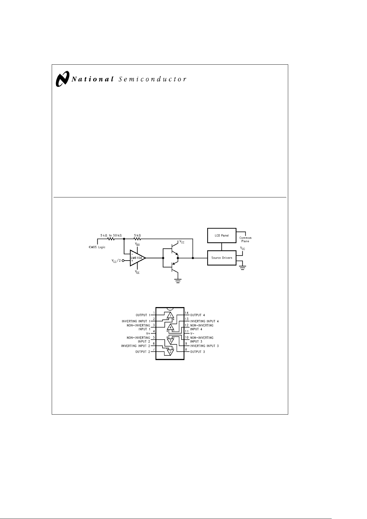
Typical Application
LCD Buffer Application for Grey Levels
TL/H/11979– 1
Connection Diagram
TL/H/11979– 2
Order Number LM6104M
See NS Package Number M14A
VIPTMis a trademark of National Semiconductor Corporation.
C
1995 National Semiconductor Corporation RRD-B30M115/Printed in U. S. A.
Page 2
Absolute Maximum Ratings (Note 1)
If Military/Aerospace specified devices are required,
please contact the National Semiconductor Sales
Office/Distributors for availability and specifications.
Supply Voltage 24V
Differential Input Voltage
g
6V
Input Voltage
g
Supply Voltage
Inverting Input Current 15 mA
Soldering Information
Vapor Phase (60s) 215
§
C
Infrared (15s) 220
§
C
Storage Temperature Range
b
65§CsT
J
s
a
150§C
Maximum Junction Temperature 150§C
ESD Rating (Note 2) 2000V
Operating Ratings
Supply Voltage Range 4.75V to 24V
Junction Temperature Range (Note 3)
LM6104M
b
20
§
s
T
J
s
a
80§C
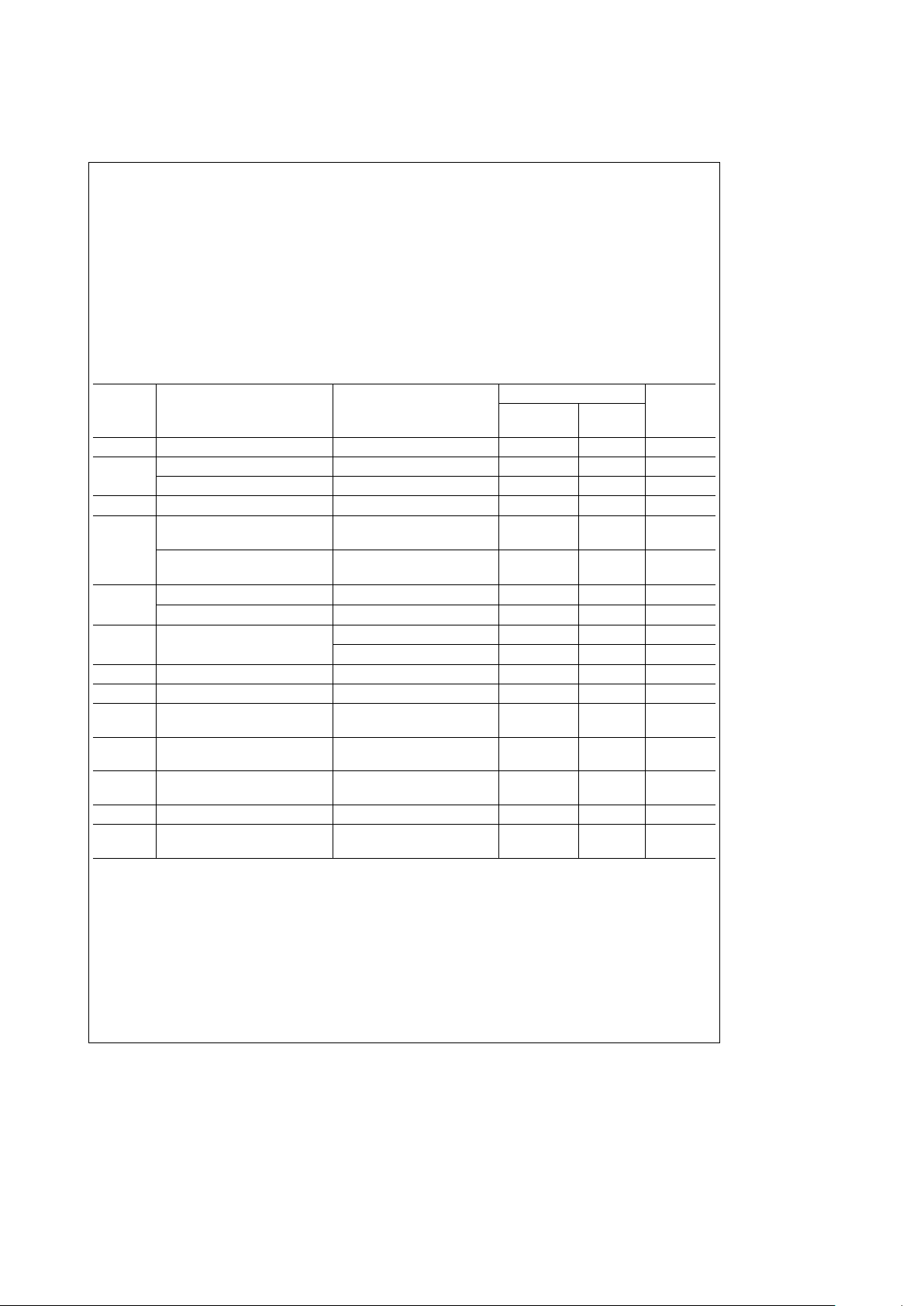
Electrical Characteristics
The following specifications apply for Vae8V, V
beb
5V, R
L
e
R
F
e
2kXand 0
§
s
T
J
s
60§C unless otherwise noted.
Symbol Parameter Conditions
LM6104M
Units
Typical Limits
(Note 4) (Note 5)
V
OS
Input Offset Voltage 10 30 mV max
I
B
Inverting Input Bias Current 5.0 20 mA max
Non-Inverting Input Bias Current 0.5 2 mA max
I
S
Supply Current V
O
e
0V 3.5 4.0 mA max
I
SC
Output Source Current V
O
e
0V
60 45
mA
I
IN(b)
eb
100 mA min
Output Sink Current V
O
e
0V
60 45
mA
I
IN(b)
e
100 mA min
V
O
Positive Output Swing I
IN(b)
eb
100 mA 6.5 6.1 V min
Negative Output Swing I
IN(b)
e
100 mA
b
3.5
b
3.1 V max
PSRR Power Supply Rejection Ratio V
S
e
g
4tog10V 70 60 dB min
100 mV pp@100 kHz 40 30 dB min
R
T
Transresistance 10 5 MX min
SR Slew Rate (Note 6) 100 55 V/ms min
BW Bandwidth A
V
eb
1
7.5 5.0 MHz
R
IN
e
R
F
e
2kX
Amp-to-Amp Isolation R
L
e
2kX
60 dB
F
e
1 MHz
CMVR Common Mode Voltage Range V
a
b
1.4V
V
V
b
a
1.4V
CMRR Common Mode Rejection Ratio 60 dB
t
S
Settling Time 0.05%, 5V Step, A
V
eb
1
240 ns
R
F
e
R
S
e
2kX,V
S
e
g
5V
Note 1: Absolute Maximum Ratings indicate limits beyond which damage to the device may occur. DC and AC electrical specifications do not apply when operating
the device beyond its rated operating conditions. Operating ratings indicate conditions the device is intended to be functional, but device parameter specifications
may not be guaranteed under the conditions.
Note 2: Human body model 1.5 kX and 100 pF. This is a class 2 device rating.
Note 3: Thermal resistance of the SO package is 98
§
C/W. When operating at T
A
e
80§C, maximum power dissipation is 700 mW.
Note 4: Typical values represent the most likely parametric norm.
Note 5: All limits guaranteed at operating temperature extremes.
Note 6: A
V
eb
1 with R
IN
e
R
F
e
2kX. Slew rate is calculated from the 25% to the 75% point on both rising and falling edges. Output swing isb0.6V toa5.6V
and 5.6V to 0.6V.
2
Page 3

Typical Performance Characteristics
Closed Loop Gain
Frequency Response vs
Amplifier Isolation
Amplifier to
Supply Voltage
Supply Current vs
A
V
eb
1
Large Signal Pulse Response
A
V
eb
1, R
F
e
R
G
Frequency Response vs R
F
I
IN
e
g
100 mA
V
S
e
g
5V
V
OUT
Referred to Supplies
vs Source Current
LM6104 Output Voltage
vs Sink Current
LM6104 Output Voltage
TL/H/11979– 3
3
Page 4

Applications Information
CURRENT FEEDBACK TOPOLOGY
The small-signal bandwidth of conventional voltage feedback amplifiers is inversely proportional to the closed-loop
gain based on the gain-bandwidth concept. In contrast, the
current feedback amplifier topology, such as the LM6104,
enables a signal bandwidth that is relatively independent of
the amplifier’s gain (see typical curve Frequency Response
vs Closed Loop Gain).
FEEDBACK RESISTOR SELECTION: R
F
Current feedback amplifier bandwidth and slew rate are
controlled by R
F.RF
and the amplifier’s internal compensation capacitor set the dominant pole in the frequency response. The amplifier, therefore, always requires a feedback resistor, even in unity gain.
Bandwidth and slew rate are inversely proportional to the
value of R
F
(see typical curve Frequency Response vs RF).
This makes the amplifier especially easy to compensate for
a desired pulse response (see typical curve Large Signal
Pulse Response). Increased capacitive load driving capability is also achieved by increasing the value of R
F
.
The LM6104 has guaranteed performance with a feedback
resistor of 2 kX.
CAPACITIVE FEEDBACK
It is common to place a small lead capacitor in parallel with
feedback resistance to compensate voltage feedback amplifiers. Do not place a capacitor across R
F
to limit the bandwidth of current feedback amplifiers. The dynamic impedance of capacitors in the feedback path of the LM6104, as
with any current feedback amplifier, will cause instability.
4
Page 5

5
Page 6

LM6104 Quad Gray Scale Current Feedback Amplifier
Physical Dimensions inches (millimeters)
14-Pin SO Package
Order Number LM6104M
NS Package Number M14A
LIFE SUPPORT POLICY
NATIONAL’S PRODUCTS ARE NOT AUTHORIZED FOR USE AS CRITICAL COMPONENTS IN LIFE SUPPORT
DEVICES OR SYSTEMS WITHOUT THE EXPRESS WRITTEN APPROVAL OF THE PRESIDENT OF NATIONAL
SEMICONDUCTOR CORPORATION. As used herein:
1. Life support devices or systems are devices or 2. A critical component is any component of a life
systems which, (a) are intended for surgical implant support device or system whose failure to perform can
into the body, or (b) support or sustain life, and whose be reasonably expected to cause the failure of the life
failure to perform, when properly used in accordance support device or system, or to affect its safety or
with instructions for use provided in the labeling, can effectiveness.
be reasonably expected to result in a significant injury
to the user.
National Semiconductor National Semiconductor National Semiconductor National Semiconductor
Corporation Europe Hong Kong Ltd. Japan Ltd.
1111 West Bardin Road Fax: (
a
49) 0-180-530 85 86 13th Floor, Straight Block, Tel: 81-043-299-2309
Arlington, TX 76017 Email: cnjwge@tevm2.nsc.com Ocean Centre, 5 Canton Rd. Fax: 81-043-299-2408
Tel: 1(800) 272-9959 Deutsch Tel: (
a
49) 0-180-530 85 85 Tsimshatsui, Kowloon
Fax: 1(800) 737-7018 English Tel: (
a
49) 0-180-532 78 32 Hong Kong
Fran3ais Tel: (
a
49) 0-180-532 93 58 Tel: (852) 2737-1600
Italiano Tel: (
a
49) 0-180-534 16 80 Fax: (852) 2736-9960
National does not assume any responsibility for use of any circuitry described, no circuit patent licenses are implied and National reserves the right at any time without notice to change said circuitry and specifications.
 Loading...