

Page 1
LM56
Dual Output Low Power Thermostat
LM56 Dual Output Low Power Thermostat
April 2000
General Description
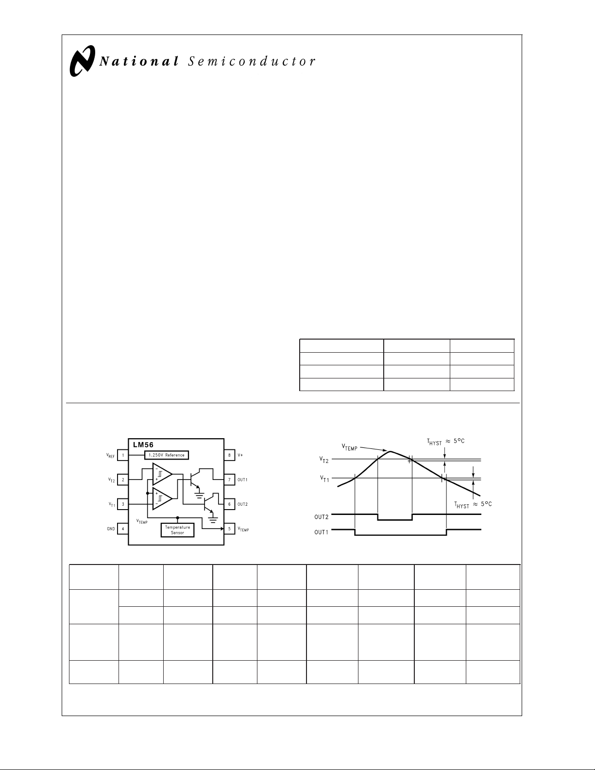
The LM56 is a precision low power thermostat. Two stable
temperature trip points (V
ing down the LM56 1.250V bandgap voltage reference using
3 external resistors. The LM56hastwodigitaloutputs.OUT1
goes LOW when the temperature exceeds T1 and goes
HIGH when the the temperature goes below (T1–T
Similarly, OUT2 goes LOW when the temperature exceeds
T2 and goes HIGH when the temperature goes below
(T2–T
The LM56 is available in an 8-lead Mini-SO8 surface mount
package and an 8-lead small outline package.
HYST
). T
is an internally set 5˚C typical hysteresis.
HYST
and VT2) are generated by divid-
T1
HYST
Applications
n Microprocessor Thermal Management
n Appliances
n Portable Battery Powered 3.0V or 5V Systems
n Fan Control
n Industrial Process Control
n HVAC Systems
n Remote Temperature Sensing
n Electronic System Protection
Features
n Digital outputs support TTL logic levels
n Internal temperature sensor
n 2 internal comparators with hysteresis
n Internal voltage reference
n Currently available in 8-pin SO plastic package
).
n Future availability in the 8-pin Mini-SO8 package
Key Specifications
n Power Supply Voltage 2.7V–10V
n Power Supply Current 230 µA (max)
n V
REF
n Hysteresis Temperature 5˚C
n Internal Temperature Sensor
Output Voltage (+6.20 mV/˚C x T) +395 mV
n Temperature Trip Point Accuracy:
+25˚C
+25˚C to +85˚C
−40˚C to +125˚C
Simplified Block Diagram and Connection Diagram
1.250V±1% (max)
LM56BIM LM56CIM
±
2˚C (max)
±
2˚C (max)
±
3˚C (max)
±
3˚C (max)
±
3˚C (max)
±
4˚C (max)
DS012893-2
DS012893-1
Order
Number
NS
Package
Number
Transport
Media
Package
Marking
© 2000 National Semiconductor Corporation DS012893 www.national.com
LM56BIM LM56BIMX LM56CIM LM56CIMX LM56BIMM LM56BIMMX LM56CIMM LM56CIMMX
M08A M08A M08A M08A MUA08A MUA08A MUA08A MUA08A
SOP-8 SOP-8 SOP-8 SOP-8 MSOP-8 MSOP-8 MSOP-8 MSOP-8
2500 Units 2500 Units 3500 Units 3500 Units
Rail Tape &
Reel
LM56BIM LM56BIM LM56CIM LM56CIM T02B T02B T02C T02C
Rail Tape &
Reel
Rail Tape & Reel Rail Tape & Reel
Page 2
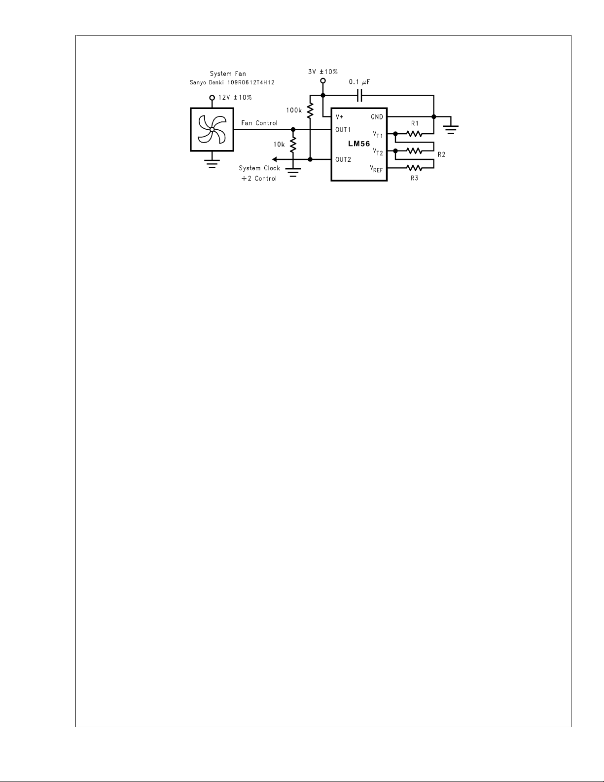
Typical Application
LM56
VT1= 1.250V x (R1)/(R1 + R2 + R3)
= 1.250V x (R1 + R2)/(R1 + R2 + R3)
V
T2
where:
(R1+R2+R3)=27kΩand
= [6.20 mV/˚C x T] + 395 mV therefore:
V
T1 or T2
/(1.25V) x 27 kΩ
R1=V
T1
R2=(V
R3=27kΩ−R1−R2
/(1.25V) x 27 kΩ)−R1
T2
DS012893-3
FIGURE 1. Microprocessor Thermal Management
www.national.com 2
Page 3

LM56
Absolute Maximum Ratings (Note 1)
Input Voltage 12V
Input Current at any pin (Note 2) 5 mA
Package Input Current(Note 2) 20 mA
Package Dissipation at T
(Note 3) 900 mW
ESD Susceptibility (Note 4)
Human Body Model 1000V
Machine Model 200V
= 25˚C
A
Vapor Phase (60 seconds) 215˚C
Infrared (15 seconds) 220˚C
Storage Temperature −65˚C to + 150˚C
Operating Ratings(Note 1)
Operating Temperature Range T
LM56BIM, LM56CIM −40˚C ≤ TA≤ +125˚C
+
Positive Supply Voltage (V
Maximum V
OUT1
and V
) +2.7V to +10V
OUT2
MIN
≤ TA≤ T
Soldering Information
SO Package (Note 5) :
LM56 Electrical Characteristics
The following specifications apply for V+= 2.7 VDC, and V
its apply for TA=TJ=T
MIN
to T
; all other limits TA=TJ= 25˚C unless otherwise specified.
MAX
Symbol Parameter Conditions (Note 6) Limits Limits (Limits)
Temperature Sensor
Trip Point Accuracy (Includes
V
, Comparator Offset, and +25˚C ≤ TA≤ +85˚C
REF
Temperature Sensitivity errors) −40˚C ≤ T
Trip Point Hysteresis T
= −40˚C 4 3 3 ˚C (min)
A
T
= +25˚C 5 3.5 3.5 ˚C (min)
A
T
= +85˚C 6 4.5 4.5 ˚C (min)
A
T
= +125˚C 6 4 4 ˚C (min)
A
Internal Temperature +6.20 mV/˚C
Sensitivity
Temperature Sensitivity Error
Output Impedance −1 µA ≤ I
Line Regulation +3.0V ≤ V
+25˚C≤T
+3.0V ≤ V
−40˚C≤T
+2.7V ≤ V
V
and VT2Analog Inputs
T1
I
BIAS
V
V
V
V
∆V
IN
OS
REF
REF
Output
REF
Analog Input Bias Current 150 300 300 nA (max)
Analog Input Voltage Range V+−1 V
Comparator Offset 2 88mV (max)
V
Nominal 1.250V V
REF
V
Error
REF
/∆V+Line Regulation +3.0V ≤ V+≤ +10V 0.13 0.25 0.25 mV/V (max)
+2.7V ≤ V
∆V
/∆ILLoad Regulation Sourcing +30 µA ≤ IL≤ +50 µA 0.15 0.15 mV/µA
REF
load current = 50 µA unless otherwise specified. Boldface lim-
REF
Typical LM56BIM LM56CIM Units
(Note 7) (Note 7)
≤ +125˚C
A
±
2
±
2
±
3
±
3 ˚C (max)
±
3 ˚C (max)
±
4 ˚C (max)
6 6 ˚C (max)
6.5 6.5 ˚C (max)
7.5 7.5 ˚C (max)
8 8 ˚C (max)
±
2
±
3
≤ +40 µA 1500 1500 Ω (max)
L
+
≤ +10V,
≤+85˚C
A
+
≤ +10V,
<
A
+
≤ +3.3V
25˚C
±
±
±
0.36
0.61
2.3
±
3 ˚C (max)
±
4 ˚C (max)
±
0.36 mV/V (max)
±
0.61 mV/V (max)
±
2.3 mV (max)
GND V
±
1
±
12.5
+
≤ +3.3V 0.15 1.1 1.1 mV (max)
±
1 % (max)
±
12.5 mV (max)
(max)
MAX
+10V
www.national.com3
Page 4

LM56 Electrical Characteristics
LM56
The following specifications apply for V+= 2.7 VDC, and V
its apply for TA=TJ=T
MIN
to T
; all other limits TA=TJ= 25˚C unless otherwise specified.
MAX
load current = 50 µA unless otherwise specified. Boldface lim-
REF
Symbol Parameter Conditions Typical Limits Units
(Note 6) (Note 7) (Limits)
+
V
Power Supply
I
S
Supply Current V+= +10V 230 µA (max)
+
V
= +2.7V 230 µA (max)
Digital Outputs
I
OUT(“1”)
Logical “1” Output Leakage V+= +5.0V 1 µA (max)
Current
V
OUT(“0”)
Note 1: Absolute MaximumRatings indicate limitsbeyond which damageto thedevice may occur. Operating Ratingsindicate conditionsfor which thedevice is functional, but do not guarantee specific performance limits. For guaranteed specifications andtest conditions, see the Electrical Characteristics. The guaranteedspecifications apply only for the test conditions listed. Some performance characteristics may degrade when the device is not operated under the listed test conditions.
Note 2: When the input voltage(V
mum package input current rating limits the number of pins that can safely exceed the power supplies with an input current of 5 mA to four.
Note 3: The maximum power dissipation must be derated at elevated temperaturesand is dictated by T
bient thermal resistance) andT
in the Absolute Maximum Ratings, whichever is lower. For this device, T
types when board mounted follow:
Logical “0” Output Voltage I
) at anypin exceeds the power supply (V
I
(ambient temperature). Themaximum allowable power dissipation at any temperatureis PD=(T
A
= +50 µA 0.4 V (max)
OUT
<
GND or V
I
= 125˚C. For this device the typical thermal resistance (θJA) of the different package
Jmax
>
V+), the currentat that pin should be limitedto 5 mA. The 20mA maxi-
I
Jmax
(maximum junction temperature), θJA(junction to am-
)/θJAor the number given
Jmax–TA
Package Type θ
JA
M08A 110˚C/W
MUA08A 250˚C/W
Note 4: The humanbody model isa 100 pFcapacitor discharge througha 1.5kΩ resistor intoeach pin. Themachine modelis a 200pF capacitor dischargeddirectly
into each pin.
Note 5: See AN450“Surface Mounting Methods andTheir Effects onProduct Reliability” or thesection titled “Surface Mount”found in anypost 1986 National Semiconductor Linear Data Book for other methods of soldering surface mount devices.
Note 6: Typicals are at T
Note 7: Limits are guaranteed to National’s AOQL(Average Outgoing Quality Level).
= 25˚C and represent most likely parametric norm.
J=TA
www.national.com 4
Page 5

Typical Performance Characteristics
LM56
Quiescent Current vs
Temperature
Trip Point Hysteresis vs
Temperature
DS012893-4
V
Output Voltage vs
REF
Load Current
Temperature Sensor
Output Voltage vs
Temperature
OUT1 and OUT2 Voltage
Levels vs Load Current
DS012893-5
DS012893-32
Temperature Sensor
Output Accuracy vs
Temperature
Trip Point
Accuracy vs Temperature
DS012893-7
DS012893-10
Comparator Bias Current
vs Temperature
DS012893-8
DS012893-11
DS012893-9
OUT1 and OUT2 Leakage
Current vs Temperature
DS012893-12
www.national.com5
Page 6

Typical Performance Characteristics (Continued)
LM56
V
Output
TEMP
Line Regulation vs Temperature
DS012893-31
V
Start-Up Response
REF
V
Start-Up Response
TEMP
DS012893-13
DS012893-14
www.national.com 6
Page 7

Functional Description
LM56
1.0 PIN DESCRIPTION
+
V
This is the positive supply voltage pin. This pin
should be bypassed with 0.1 µF capacitor to
ground.
GND This is the ground pin.
V
REF
This is the 1.250V bandgap voltage reference out-
put pin. In order to maintain trip point accuracy this
pin should source a 50 µA load.
V
TEMP
This is the temperature sensor output pin.
OUT1 Thisisanopen collector digital output. OUT1 is ac-
tive LOW. It goes LOW when the temperature is
greater than T
ture drops below T
and goes HIGH when the tempera-
1
–5˚C. This output is not in-
1
tended to directly drive a fan motor.
OUT2 Thisisanopen collector digital output. OUT2 is ac-
tive LOW. It goes LOW when the temperature is
greater than the T
the temperature is less than T
set point and goes HIGH when
2
–5˚C. This output is
2
not intended to directly drive a fan motor.
V
T1
This is the input pin for the temperature trip point
voltage for OUT1.
V
T2
This is the input pin for the low temperature trip
point voltage for OUT2.
VT1= 1.250V x (R1)/(R1 + R2 + R3)
= 1.250V x (R1 + R2)/(R1 + R2 + R3)
V
T2
where:
(R1+R2+R3)=27kΩand
= [6.20 mV/˚C x T] + 395 mV therefore:
V
T1 or T2
/(1.25V) x 27 kΩ
R1=V
T1
R2=(V
R3=27kΩ−R1−R2
/(1.25V) x 27 k)Ω–R1
T2
DS012893-15
DS012893-16
www.national.com7
Page 8

Application Hints
LM56
2.0 LM56 TRIP POINT ACCURACY SPECIFICATION
For simplicity the following is an analysis of the trip point accuracy using the single output configuration show in
with a set point of 82˚C.
Trip Point Error Voltage = V
Comparator Offset Error for V
Temperature Sensor Error = V
Reference Output Error = V
TPE
RE
,
T1E
TSE
FIGURE 2. Single Output Configuration
Figure 2
DS012893-17
±
range of −40˚C to +125˚C, for example, is specified at
3˚C
for the LM56BIM. Note this trip point error specification does
not include any error introduced by the tolerance of the actual resistors used, nor any error introduced by power supply
variation.
If the resistors have a
±
0.4˚C will be introduced. This error will increase to±0.8˚C
when both external resistors have a
±
0.5% tolerance, an additional errorof
±
1% tolerance.
3.0 BIAS CURRENT EFFECT ON
TRIP POINT ACCURACY
Bias current for the comparator inputs is 300 nA (max) each,
over the specified temperature range and will not introduce
considerable error if the sum of the resistor values are kept
to about 27 kΩ as shown in the typical application of
1
. This bias current of one comparator input will not flow if
Figure
the temperature is well below the trip point level. As the temperature approaches trip point level the bias current will start
to flow into the resistor network. When the temperature sensor output is equal to the trip point level the bias current will
be 150 nA(max).Oncethe temperature is well above the trip
point level the bias current will be 300 nA (max). Therefore,
the first trip point will be affected by 150 nA of bias current.
The leakage current is very small when the comparator input
transistor of the different pair is off (see
Figure 3
).
The effect of the bias current on the first trip point can be defined by the following equations:
1. V
TPE
=±V
T1E−VTSE+VRE
Where:
2. V
3. V
4. V
=±8 mV (max)
T1E
= (6.20 mV/˚C) x (±3˚C) =±18.6 mV
TSE
= 1.250V x (±0.01) R2/(R1 + R2)
RE
Using Equations from page 1 of the datasheet.
V
=1.25VxR2/(R1+R2)=(6.20 mV/˚C)(82˚C) +395 mV
T1
Solving for R2/(R1 + R2) = 0.7227
then,
5. V
(0.7227) =
= 1.250V x (±0.01) R2/(R1 + R2) = (0.0125) x
RE
±
9.03 mV
The individual errors do not add algebraically because, the
odds of all the errors being at their extremes are rare. This is
proven by the fact the specification for the trip point accuracy
stated in the Electrical Characteristic for the temperature
where IB= 300 nA (the maximum specified error).
The effect of the bias current on the second trip point can be
defined by the following equations:
where IB= 300 nA (the maximum specified error).
The closer the two trip points are to each other the more sig-
nificant the error is. Worst case would be when V
V
/2.
REF
T1=VT2
=
www.national.com 8
Page 9

Application Hints (Continued)
LM56
FIGURE 3. Simplified Schematic
4.0 MOUNTING CONSIDERATIONS
The majority of the temperature that the LM56 is measuring
is the temperature of its leads. Therefore, when the LM56 is
placed on a printed circuit board, it is not sensing the temperature of the ambient air. It is actually sensing the temperature differenceoftheairandthe lands and printed circuit
board that the leads are attached to. The most accurate temperature sensing is obtained when the ambient temperature
is equivalent to the LM56’s lead temperature.
DS012893-18
As with any IC, the LM56 and accompanying wiring and circuits must be kept insulated and dry, to avoid leakage and
corrosion. This is especially true if the cirucit may operate at
cold temperatures where condensation can occur.
Printed-circuit coatings and varnishes such as Humiseal and
epoxy paints or dips are often used to ensure that moisture
cannot corrode the LM56 or its connections.
www.national.com9
Page 10

Application Hints (Continued)
LM56
5.0 V
REF
AND V
CAPACTIVE LOADING
TEMP
FIGURE 4. Loading of V
The LM56 V
REF
and V
outputs handle capacitive load-
TEMP
ing well. Without any special precautions, these outputs can
drive any capacitive load as shown in
Figure 4
6.0 NOISY ENVIRONMENTS
Over the specified temperature range the LM56 V
put has a maximum output impedance of 1500Ω.Inanextremely noisy environment it may be necessary to add some
filtering to minimize noise pickup. It is recommended that 0.1
µF be added from V
voltage, as shown in
be necessary to add a capacitor from the V
+
to GND to bypass the power supply
Figure 4
. In a noisy environment it may
TEMP
ground. A 1 µF output capacitor with the 1500Ω output impedance will form a 106 Hz lowpass filter. Since the thermal
time constant of the V
output is much slower than the
TEMP
9.4 ms time constant formed by the RC, the overall response
time of the V
output will not be significantly affected. For
TEMP
much larger capacitors this additional time lag will increase
the overall response time of the LM56.
.
TEMP
output to
out-
DS012893-19
and V
REF
The circuit shown in
current error for V
equivalent to the error term of V
TEMP
Figure 5
T2
will reduce the effective bias
as discussed in Section 3.0 to be
. For this circuit the effect
T1
of the bias current on the first trip point can be defined by the
following equations:
where IB= 300 nA (the maximum specified error).
Similarly, bias current affect on V
can be defined by:
T2
7.0 APPLICATIONS CIRCUITS
DS012893-20
FIGURE 5. Reducing Errors Caused by Bias Current
www.national.com 10
where IB= 300 nA (the maximum specified error).
The current shown in
Figure 6
is a simple overtemperature
detector for power devices. In this example, an audio power
amplifier IC is bolted to a heat sink and an LM56 Celsius
temperature sensor is mounted on a PC board that is bolted
to the heat sink near the power amplifier. To ensure that the
sensing element isatthesametemperature as the heat sink,
the sensor’s leads are mounted to pads that have feed
throughs to the back side of the PC board. Since the LM56 is
sensing the temperature of the actual PC board the back
side of the PC board also has large ground plane to help
conduct the heat to the device. The comparator’s output
goes low if the heatsinktemperaturerisesaboveathreshold
set by R1, R2, and the voltage reference. This fault detection
output from the comparator now can be used to turn on a
cooling fan. The circuit as shown in design to turn the fan on
when heat sink temperature exceeds about 80˚C,andtoturn
the fan off when the heat sink temperature falls below approximately 75˚C.
Page 11

Application Hints (Continued)
LM56
FIGURE 6. Audio Power Amplifier Overtemperature Detector
FIGURE 7. Simple Thermostat
DS012893-21
DS012893-22
www.national.com11
Page 12

Physical Dimensions inches (millimeters) unless otherwise noted
LM56
8-Lead (0.150" Wide) Molded Small Outline Package, JEDEC
Order Number LM56BIM, LM56BIMX, LM56CIM or LM56CIMX
NS Package Number M08A
www.national.com 12
Page 13

Physical Dimensions inches (millimeters) unless otherwise noted (Continued)
LM56 Dual Output Low Power Thermostat
8-Lead Molded Mini Small Outline Package (MSOP)
(JEDEC REGISTRATION NUMBER M0-187)
Order Number LM56BIMM, LM56BIMMX, LM56CIMM, or LM56CIMMX
NS Package Number MUA08A
LIFE SUPPORT POLICY
NATIONAL’S PRODUCTS ARE NOT AUTHORIZED FOR USE AS CRITICAL COMPONENTS IN LIFE SUPPORT
DEVICES OR SYSTEMS WITHOUT THE EXPRESS WRITTEN APPROVAL OF THE PRESIDENT AND GENERAL
COUNSEL OF NATIONAL SEMICONDUCTOR CORPORATION. As used herein:
1. Life support devices or systems are devices or
systems which, (a) are intended for surgical implant
into the body, or (b) support or sustain life, and
whose failure to perform when properly used in
accordance with instructions for use provided in the
2. A critical component is any component of a life
support device or system whose failure to perform
can be reasonably expected to cause the failure of
the life support device or system, or to affect its
safety or effectiveness.
labeling, can be reasonably expected to result in a
significant injury to the user.
National Semiconductor
Corporation
Americas
Tel: 1-800-272-9959
Fax: 1-800-737-7018
Email: support@nsc.com
www.national.com
National Semiconductor
Europe
Fax: +49 (0) 180-530 85 86
Email: europe.support@nsc.com
Deutsch Tel: +49 (0) 69 9508 6208
English Tel: +44 (0) 870 24 0 2171
Français Tel: +33 (0) 1 41 91 8790
National Semiconductor
Asia Pacific Customer
Response Group
Tel: 65-2544466
Fax: 65-2504466
Email: ap.support@nsc.com
National Semiconductor
Japan Ltd.
Tel: 81-3-5639-7560
Fax: 81-3-5639-7507
National does not assume any responsibility for use of any circuitry described, no circuit patent licenses are implied and National reserves the right at any time without notice to change said circuitry and specifications.
 Loading...