

Page 1
LM567/LM567C
Tone Decoder
General Description
The LM567 and LM567C are general purpose tone decoders
designed to provide a saturated transistor switch to ground
when an input signal is present within the passband. The circuit consists of an I and Q detector driven by a voltage controlled oscillator which determines the center frequency of
the decoder. External components are used to independently set center frequency, bandwidth and output delay.
Features
n 20 to 1 frequency range with an external resistor
n Logic compatible output with 100 mA current sinking
capability
n Bandwidth adjustable from 0 to 14
Connection Diagrams
%
LM567/LM567C Tone Decoder
May 1999
n High rejection of out of band signals and noise
n Immunity to false signals
n Highly stable center frequency
n Center frequency adjustable from 0.01 Hz to 500 kHz
Applications
n Touch tone decoding
n Precision oscillator
n Frequency monitoring and control
n Wide band FSK demodulation
n Ultrasonic controls
n Carrier current remote controls
n Communications paging decoders
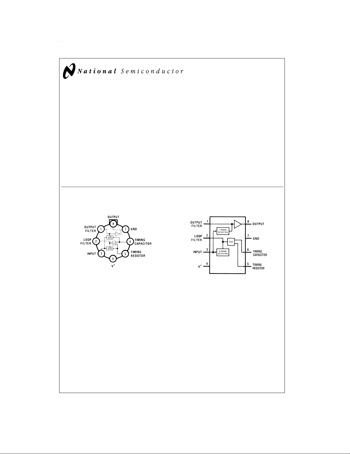
Metal Can Package
DS006975-1
Top View
Order Number LM567H or LM567CH
See NS Package Number H08C
Dual-In-Line and Small Outline Packages
DS006975-2
Top View
Order Number LM567CM
See NS Package Number M08A
Order Number LM567CN
See NS Package Number N08E
© 1999 National Semiconductor Corporation DS006975 www.national.com
Page 2

Absolute Maximum Ratings (Note 1)
If Military/Aerospace specified devices are required,
please contact the National Semiconductor Sales Office/
Distributors for availability and specifications.
Supply Voltage Pin 9V
Power Dissipation (Note 2) 1100 mW
V
8
V
3
V
3
Storage Temperature Range −65˚C to +150˚C
15V
−10V
V4+ 0.5V
Operating Temperature Range
LM567H −55˚C to +125˚C
LM567CH, LM567CM, LM567CN 0˚C to +70˚C
Soldering Information
Dual-In-Line Package
Soldering (10 sec.) 260˚C
Small Outline Package
Vapor Phase (60 sec.) 215˚C
Infrared (15 sec.) 220˚C
See AN-450 “Surface Mounting Methods and Their Effect
on Product Reliability” for other methods of soldering
surface mount devices.
Electrical Characteristics
25˚C, V
+
=
5V
LM567 LM567C/LM567CM
Min Typ Max Min Typ Max
= 20k 6 8 7 10 mA
L
= 20k 11 13 12 15 mA
L
= 100 mA, fi=f
L
= 100 mA, fi=f
C
o
o
20 25 20 25 mVrms
10 15 10 15 mVrms
Units
66dB
B
= 140 kHz
n
4.75–6.75V
<
<
T
70
A
<
<
T
−55
+125
A
4.75V–6.75V
4.75V–9V
= 15V 0.01 25 0.01 25 µA
8
= 25 mV, I8=30mA
i
= 25 mV, I8= 100 mA
e
i
−6 −6 dB
±
0.1
±
±
1
2
±
35
60
±
35
140
0.5 1.0
2.0
/20 fo/20
o
0.2
0.4
0.6
1.0
±
0.1
±
1
±
60
35
±
35
140
0.4 2.0
0.2
0.6
±
2.0
0.4
1.0
5
%
of f
%
of f
%
%
ppm/˚C
ppm/˚C
%
%
V
AC Test Circuit, T
=
A
Parameters Conditions
Power Supply Voltage Range 4.75 5.0 9.0 4.75 5.0 9.0 V
Power Supply Current Quiescent R
Power Supply Current Activated R
Input Resistance 18 20 15 20 kΩ
Smallest Detectable Input Voltage I
Largest No Output Input Voltage I
Largest Simultaneous Outband Signal to
Inband Signal Ratio
Minimum Input Signal to Wideband Noise
Ratio
Largest Detection Bandwidth 12 14 16 10 14 18
Largest Detection Bandwidth Skew 1 2 2 3
Largest Detection Bandwidth Variation
with Temperature
Largest Detection Bandwidth Variation
with Supply Voltage
Highest Center Frequency 100 500 100 500 kHz
Center Frequency Stability (4.75–5.75V) 0
Center Frequency Shift with Supply
Voltage
Fastest ON-OFF Cycling Rate f
Output Leakage Current V
Output Saturation Voltage e
Output Fall Time 30 30 ns
Output Rise Time 150 150 ns
Note 1: Absolute Maximum Ratings indicate limits beyond which damage to the device may occur. Operating Ratings indicate conditions for which the device is functional, but do not guarantee specific performance limits. Electrical Characteristics state DC andAC electrical specifications under particular test conditions which guarantee specific performance limits. This assumes that the device is within the Operating Ratings. Specifications are not guaranteed for parameters where no limit is
given, however, the typical value is a good indication of device performance.
Note 2: The maximum junction temperature of the LM567 and LM567C is 150˚C. For operating at elevated temperatures, devices in the TO-5 package must be derated based on a thermal resistance of 150˚C/W, junction to ambient or 45˚C/W, junction to case. For the DIP the device must be derated based on a thermal resistance of 110˚C/W, junction to ambient. For the Small Outline package, the device must be derated based on a thermal resistance of 160˚C/W, junction to ambient.
Note 3: Refer to RETS567X drawing for specifications of military LM567H version.
o
o
/˚C
V
/V
/V
www.national.com 2
Page 3
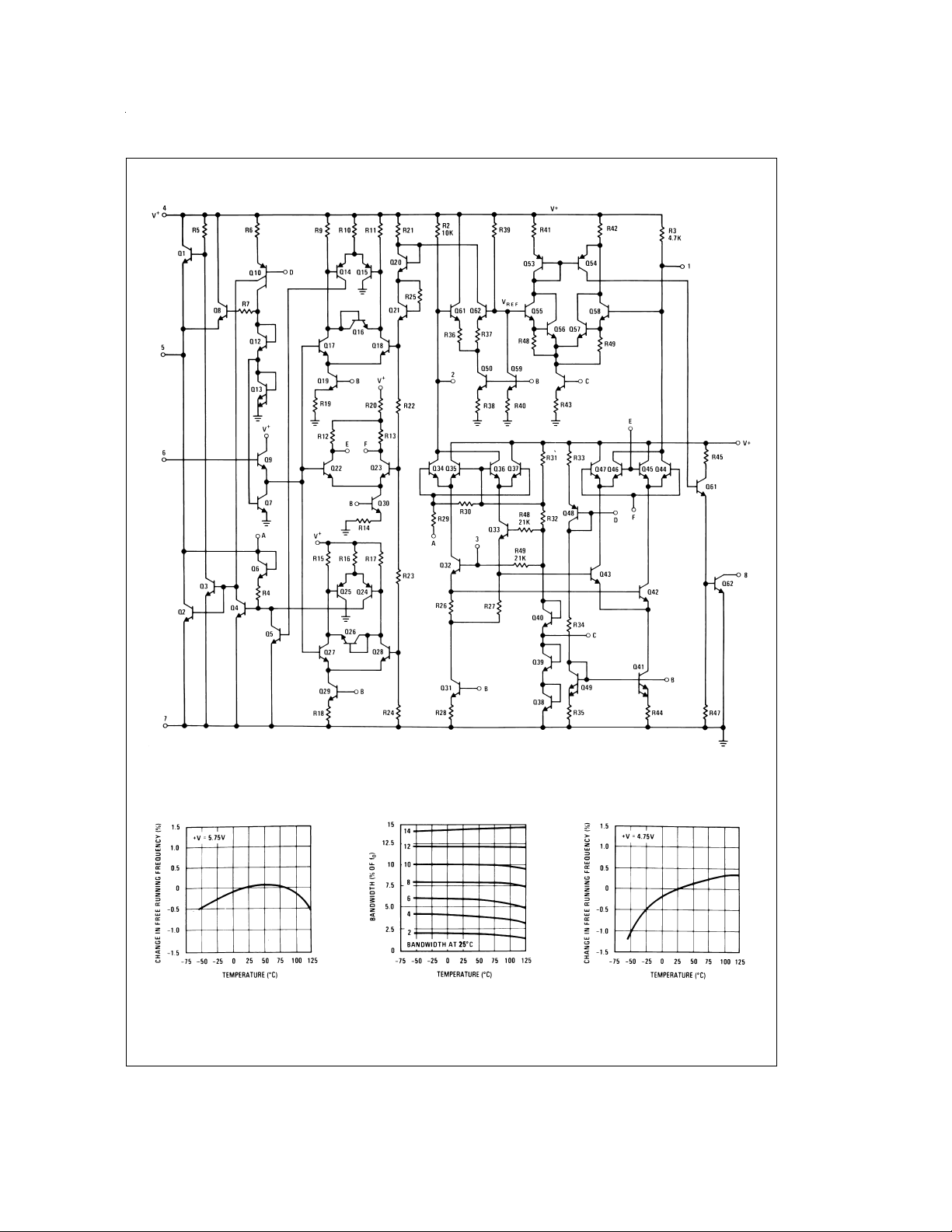
Schematic Diagram
Typical Performance Characteristics
Typical Frequency Drift
DS006975-10
Typical Bandwidth Variation
DS006975-11
DS006975-3
Typical Frequency Drift
DS006975-12
www.national.com3
Page 4
Typical Performance Characteristics (Continued)
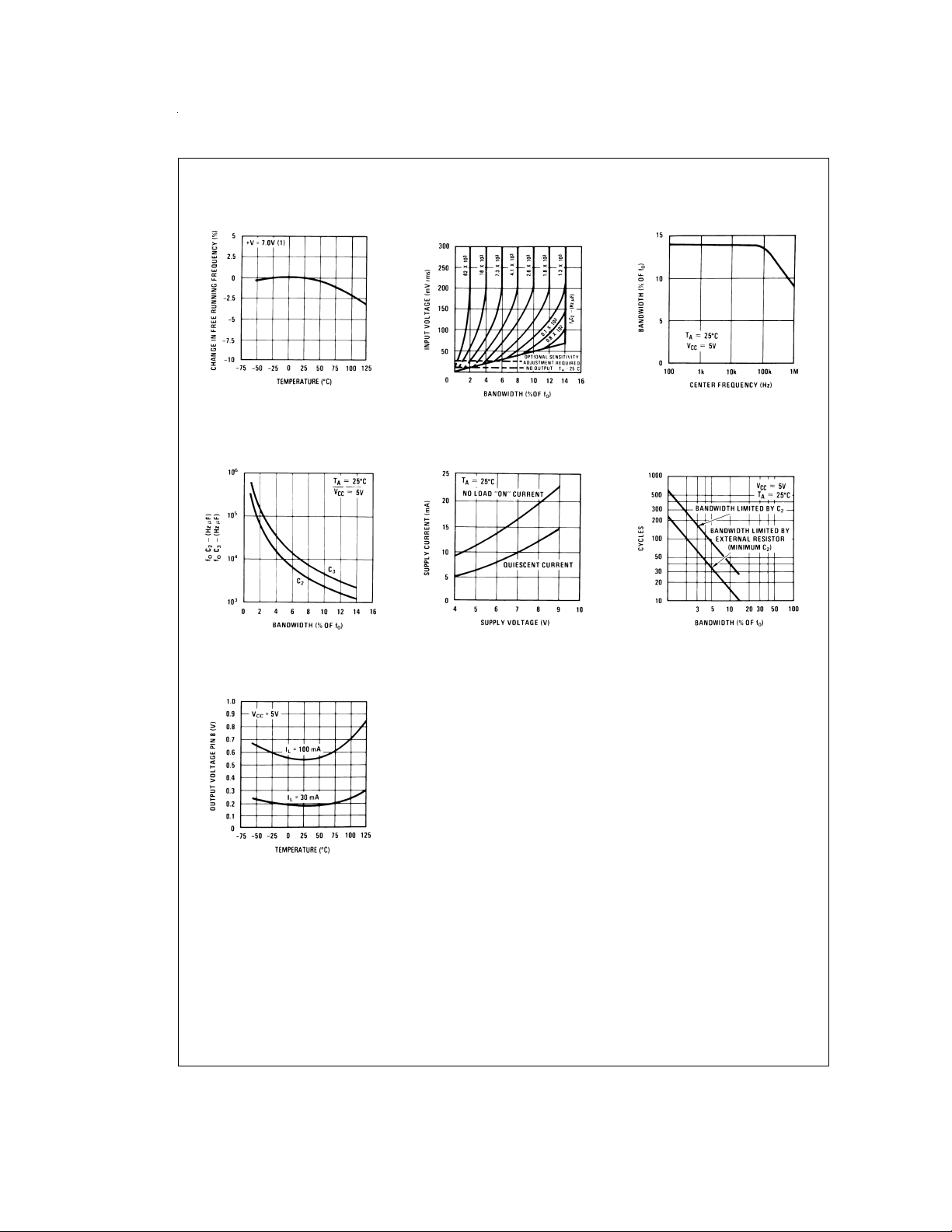
Typical Frequency Drift
Detection Bandwidth as a
Function of C
and C
2
3
DS006975-13
DS006975-16
Bandwidth vs Input Signal
Amplitude
Typical Supply Current vs
Supply Voltage
DS006975-14
DS006975-17
Largest Detection Bandwidth
DS006975-15
Greatest Number of Cycles
Before Output
DS006975-18
Typical Output Voltage vs
Temperature
DS006975-19
www.national.com 4
Page 5
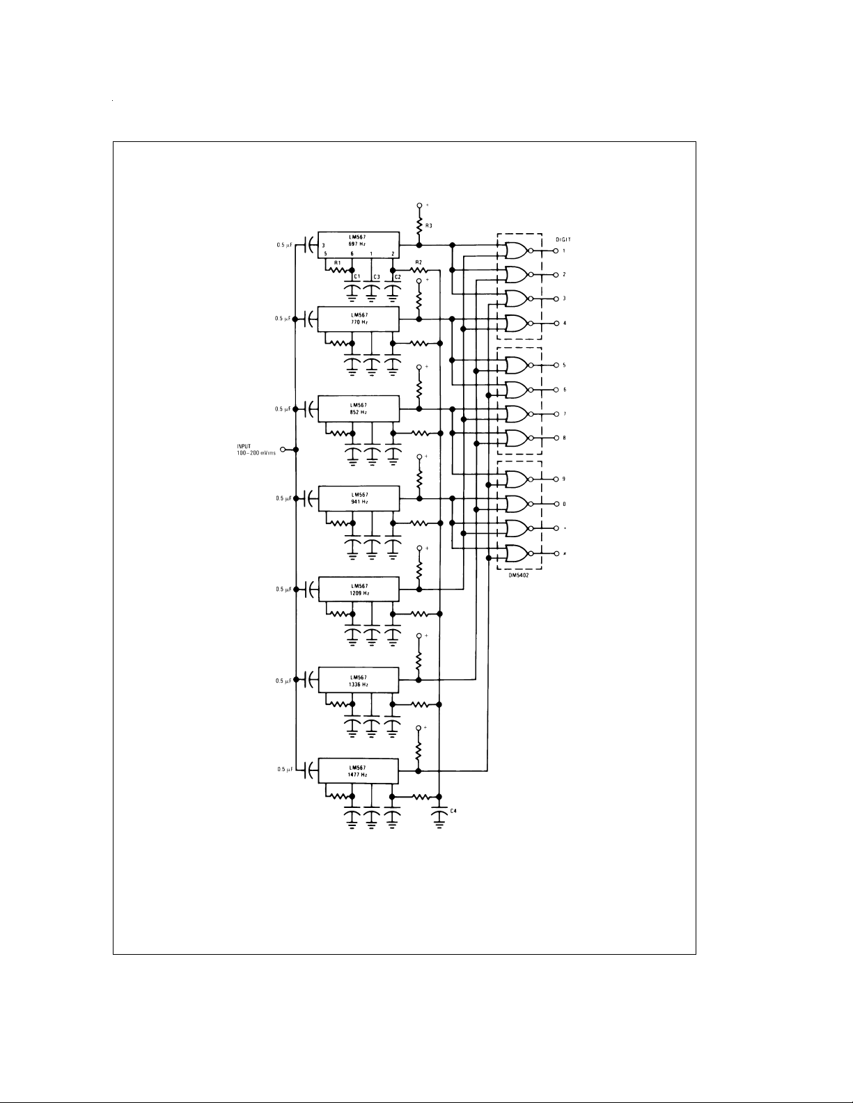
Typical Applications
Touch-Tone Decoder
Component values (typ)
R1 6.8 to 15k
R2 4.7k
R3 20k
C1 0.10 mfd
C2 1.0 mfd 6V
C3 2.2 mfd 6V
C4 250 mfd 6V
DS006975-5
www.national.com5
Page 6
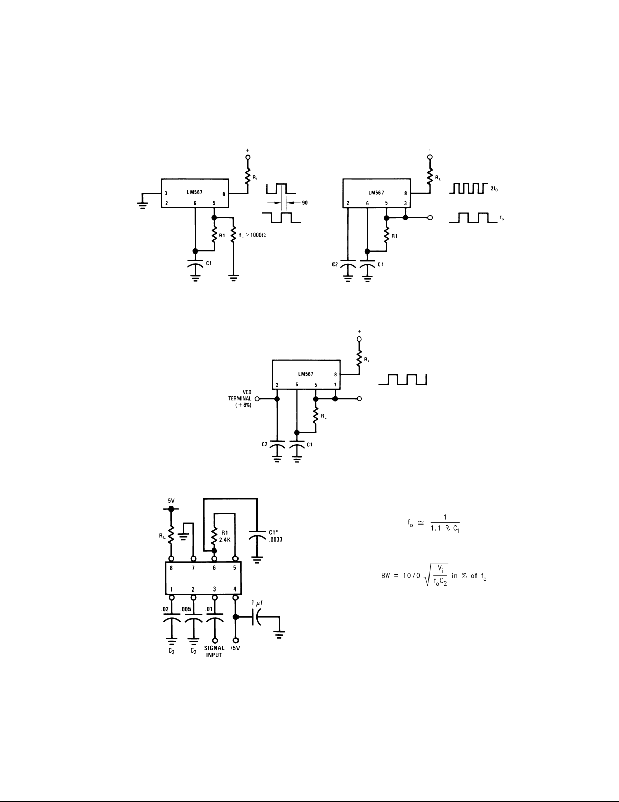
Typical Applications (Continued)
Oscillator with Quadrature Output
Connect Pin 3 to 2.8V to Invert Output
Oscillator with Double Frequency Output
DS006975-6
Precision Oscillator Drive 100 mA Loads
DS006975-7
DS006975-8
AC Test Circuit Applications Information
The center frequency of the tone decoder is equal to the free
running frequency of the VCO. This is given by
The bandwidth of the filter may be found from the approximation
Where:
=
V
Input voltage (volts rms), V
i
=
C
Capacitance at Pin 2 (µF)
2
=
f
100 kHz + 5V
i
*
Note: Adjust for f
www.national.com 6
=
o
100 kHz.
DS006975-9
≤ 200 mV
i
Page 7
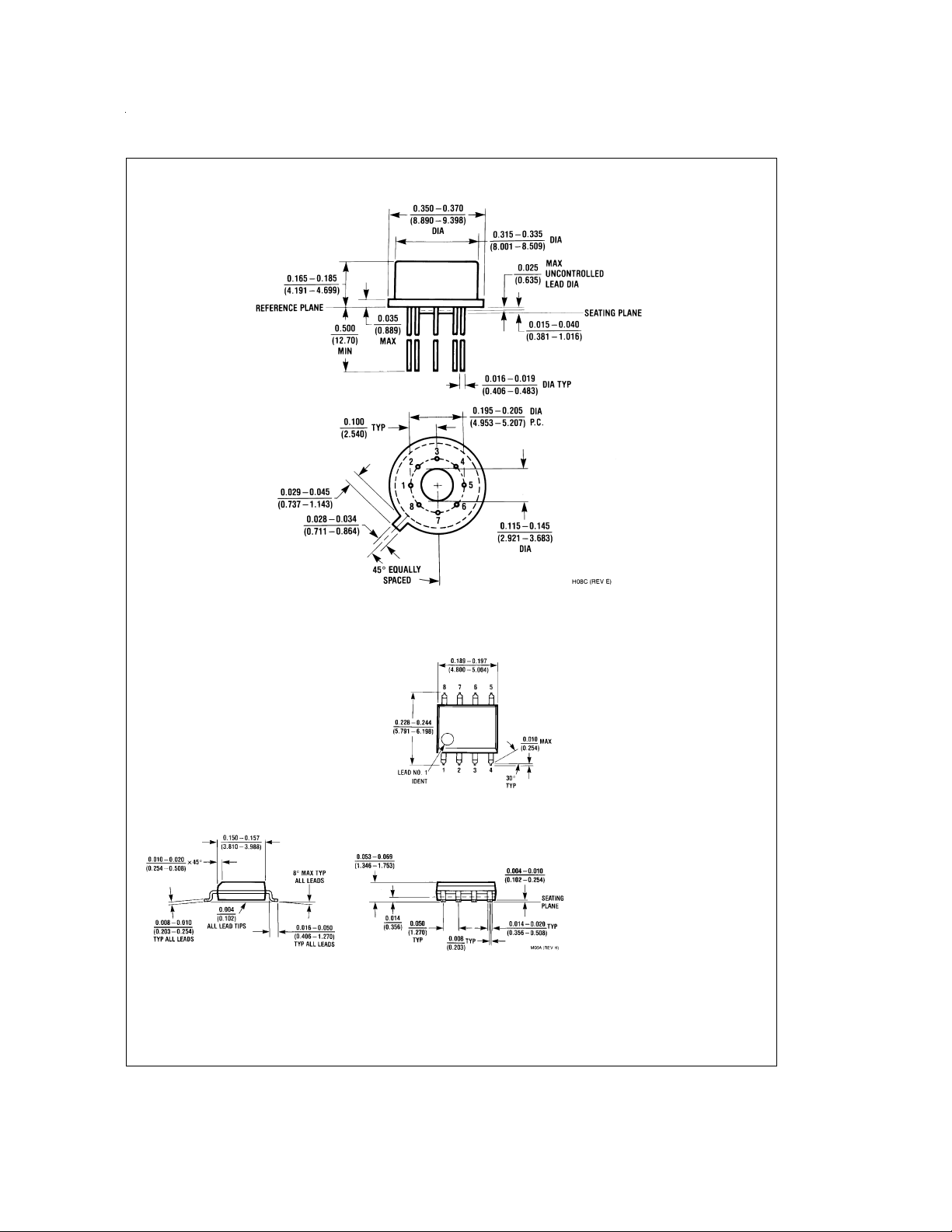
Physical Dimensions inches (millimeters) unless otherwise noted
Metal Can Package (H)
Order Number LM567H or LM567CH
NS Package Number H08C
Small Outline Package (M)
Order Number LM567CM
NS Package Number M08A
www.national.com7
Page 8
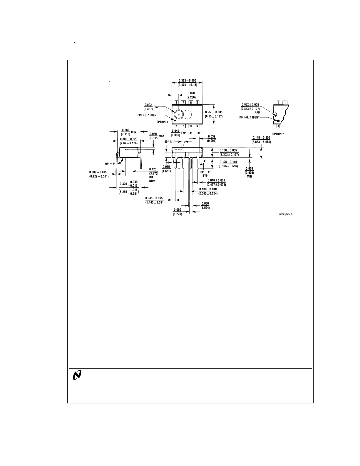
Physical Dimensions inches (millimeters) unless otherwise noted (Continued)
LM567/LM567C Tone Decoder
Molded Dual-In-Line Package (N)
Order Number LM567CN
NS Package Number N08E
LIFE SUPPORT POLICY
NATIONAL’S PRODUCTS ARE NOT AUTHORIZED FOR USE AS CRITICAL COMPONENTS IN LIFE SUPPORT
DEVICES OR SYSTEMS WITHOUT THE EXPRESS WRITTEN APPROVAL OF THE PRESIDENT AND GENERAL
COUNSEL OF NATIONAL SEMICONDUCTOR CORPORATION. As used herein:
1. Life support devices or systems are devices or
systems which, (a) are intended for surgical implant
into the body, or (b) support or sustain life, and
whose failure to perform when properly used in
accordance with instructions for use provided in the
2. A critical component is any component of a life
support device or system whose failure to perform
can be reasonably expected to cause the failure of
the life support device or system, or to affect its
safety or effectiveness.
labeling, can be reasonably expected to result in a
significant injury to the user.
National Semiconductor
Corporation
Americas
Tel: 1-800-272-9959
Fax: 1-800-737-7018
Email: [email protected]
www.national.com
National does not assume any responsibility for use of any circuitry described, no circuit patent licenses are implied and National reserves the right at any time without notice to change said circuitry and specifications.
National Semiconductor
Europe
Fax: +49 (0) 1 80-530 85 86
Email: [email protected]
Deutsch Tel: +49 (0) 1 80-530 85 85
English Tel: +49 (0) 1 80-532 78 32
Français Tel: +49 (0) 1 80-532 93 58
Italiano Tel: +49 (0) 1 80-534 16 80
National Semiconductor
Asia Pacific Customer
Response Group
Tel: 65-2544466
Fax: 65-2504466
Email: [email protected]
National Semiconductor
Japan Ltd.
Tel: 81-3-5639-7560
Fax: 81-3-5639-7507
 Loading...