

Page 1
LM565/LM565C
Phase Locked Loop
General Description
The LM565 and LM565C are general purpose phase locked
loops containing a stable,highly linear voltage controlled oscillator for low distortion FM demodulation, and a double balanced phase detector with good carrier suppression. The
VCO frequency is set with an external resistor and capacitor,
and a tuning range of 10:1 can be obtained with the same
capacitor. The characteristics of the closed loop
system—bandwidth, response speed, capture and pull in
range—may be adjusted over a wide range with an external
resistor and capacitor. The loop may be broken between the
VCO and the phase detector for insertion of a digital frequency divider to obtain frequency multiplication.
The LM565H is specified for operation over the −55˚C to
+125˚C military temperature range. The LM565CN is specified for operation over the 0˚C to +70˚C temperature range.
Features
n 200 ppm/˚C frequency stability of the VCO
n Power supply range of
typical
±
5to±12 volts with 100 ppm/
%
May 1999
n 0.2%linearity of demodulated output
n Linear triangle wave with in phase zero crossings
available
n TTL and DTL compatible phase detector input and
square wave output
n Adjustable hold in range from
±
1%to
>
±
%
60
Applications
n Data and tape synchronization
n Modems
n FSK demodulation
n FM demodulation
n Frequency synthesizer
n Tone decoding
n Frequency multiplication and division
n SCA demodulators
n Telemetry receivers
n Signal regeneration
n Coherent demodulators
LM565/LM565C Phase Locked Loop
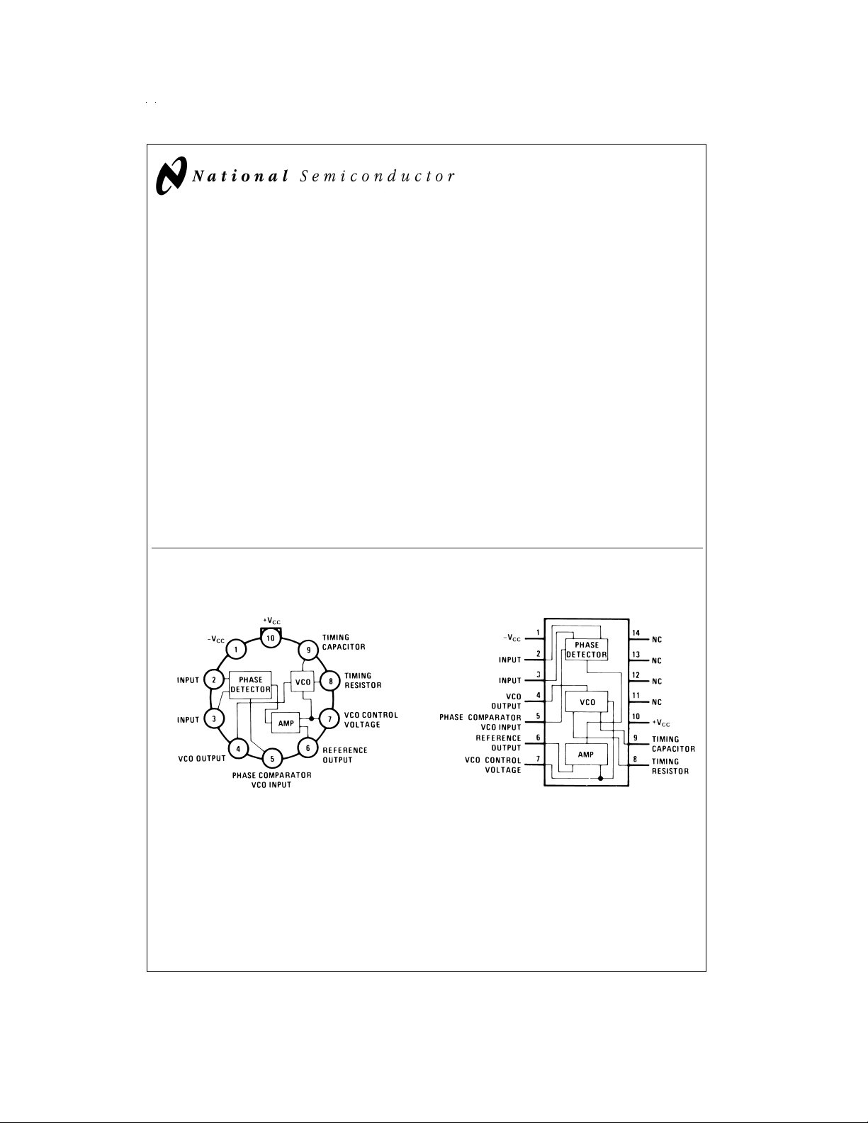
Connection Diagrams
Metal Can Package
Order Number LM565H
See NS Package Number H10C
DS007853-2
Dual-in-Line Package
DS007853-3
Order Number LM565CN
See NS Package Number N14A
© 1999 National Semiconductor Corporation DS007853 www.national.com
Page 2
Absolute Maximum Ratings (Note 1)
If Military/Aerospace specified devices are required,
please contact the National Semiconductor Sales Office/
Distributors for availability and specifications.
Supply Voltage
Power Dissipation (Note 2) 1400 mW
Differential Input Voltage
±
12V
±
Operating Temperature Range
LM565H −55˚C to +125˚C
LM565CN 0˚C to +70˚C
Storage Temperature Range −65˚C to +150˚C
Lead Temperature
(Soldering, 10 sec.) 260˚C
1V
Electrical Characteristics
AC Test Circuit, T
A
=
25˚C, V
Parameter Conditions
Power Supply Current 8.0 12.5 8.0 12.5 mA
Input Impedance (Pins 2, 3) −4V
VCO Maximum Operating
Frequency
VCO Free-Running Frequency C
Operating Frequency
Temperature Coefficient
Frequency Drift with
Supply Voltage
Triangle Wave Output Voltage 2 2.4 3 2 2.4 3 V
Triangle Wave Output Linearity 0.2 0.5
Square Wave Output Level 4.7 5.4 4.7 5.4 V
Output Impedance (Pin 4) 5 5 kΩ
Square Wave Duty Cycle 45 50 55 40 50 60
Square Wave Rise Time 20 20 ns
Square Wave Fall Time 50 50 ns
Output Current Sink (Pin 4) 0.6 1 0.6 1 mA
VCO Sensitivity f
Demodulated Output Voltage
(Pin 7)
Total Harmonic Distortion
Output Impedance (Pin 7) 3.5 3.5 kΩ
DC Level (Pin 7) 4.25 4.5 4.75 4.0 4.5 5.0 V
Output Offset Voltage
|V
|
7−V6
Temperature Drift of |V
7−V6
AM Rejection 30 40 40 dB
Phase Detector Sensitivity K
Note 1: Absolute Maximum Ratings indicate limits beyond which damage to the device may occur. Operating Ratings indicate conditions for which the device is functional, but do not guarantee specific performance limits. Electrical CharacteristicsstateDCandACelectricalspecificationsunderparticulartestconditionswhichguarantee specific performance limits. This assumes that the device is within the Operating Ratings. Specifications are not guaranteed for parameters where no limit is
given, however, the typical value is a good indication of device performance.
Note 2: The maximum junction temperature of the LM565 and LM565C is +150˚C. For operation at elevated temperatures, devices in the TO-5 package must be
derated based on a thermal resistance of +150˚C/W junction to ambient or +45˚C/W junction to case. Thermal resistance of the dual-in-line package is +85˚C/W.
=
±
6V
CC
LM565 LM565C
Min Typ Max Min Typ Max
<
<
V2,V
=
C
2.7 pF
o
=
1.5 nF
o
=
20 kΩ
R
o
=
10 kHz
f
o
0V 7 10 5 kΩ
3
300 500 250 500 kHz
−10 0 +10 −30 0 +30
Units
−100 −200 ppm/˚C
0.1 1.0 0.2 1.5
=
10 kHz 6600 6600 Hz/V
o
±
10%Frequency Deviation
±
10%Frequency Deviation 0.2 0.75 0.2 1.5
250 300 400 200 300 450 mV
%
30 100 50 200 mV
| 500 500 µV/˚C
D
0.68 0.68 V/radian
%
%
%
%
/V
p-p
p-p
p-p
www.national.com 2
Page 3
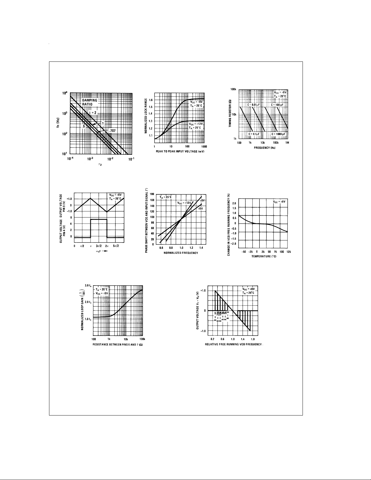
Typical Performance Characteristics
Power Supply Current as a
Function of Supply Voltage
Oscillator Output
Waveforms
DS007853-14
DS007853-17
Lock Range as a Function
of Input Voltage
Phase Shift vs Frequency
DS007853-15
DS007853-18
VCO Frequency
DS007853-16
VCO Frequency as a
Function of Temperature
DS007853-19
Loop Gain vs Load
Resistance
DS007853-20
Hold in Range as a
Function of R
6–7
DS007853-21
www.national.com3
Page 4
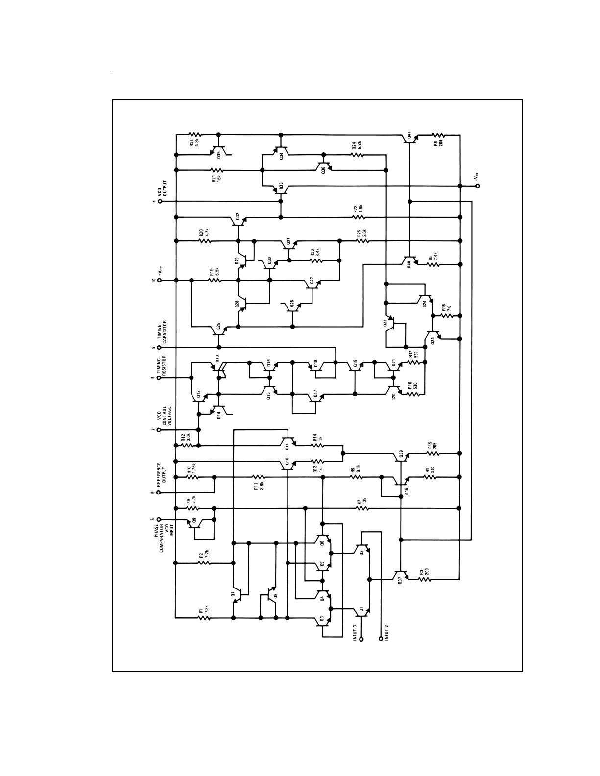
Schematic Diagram
DS007853-1
www.national.com 4
Page 5

AC Test Circuit
Note: S1open for output offset voltage (V7−V6) measurement.
Typical Applications
2400 Hz Synchronous AM Demodulator
DS007853-5
DS007853-6
www.national.com5
Page 6

Typical Applications (Continued)
FSK Demodulator (2025–2225 cps)
FSK Demodulator with DC Restoration
DS007853-7
www.national.com 6
DS007853-8
Page 7

Typical Applications (Continued)
Frequency Multiplier (x10)
DS007853-9
IRIG Channel 13 Demodulator
DS007853-10
www.national.com7
Page 8

Applications Information
In designing with phase locked loops such as the LM565, the
important parameters of interest are:
FREE RUNNING FREQUENCY
LOOP GAIN: relates the amount of phase change between
the input signal and the VCO signal for a shift in input signal
frequency (assuming the loop remains in lock). In servo
theory, this is called the “velocity error coefficient.”
The loop gain of the LM565 is dependent on supply voltage,
and may be found from:
Lag-Lead Filter
DS007853-12
A simple lag filter may be used for wide closed loop bandwidth applications such as modulation following where the
frequency deviation of the carrier is fairly high (greater than
10%), or where wideband modulating signals must be followed.
The natural bandwidth of the closed loop response may be
found from:
Associated with this is a damping factor:
=
f
VCO frequency in Hz
o
=
total supply voltage to circuit
V
c
Loop gain may be reduced by connecting a resistor between
pins 6 and 7; this reduces the load impedance on the output
amplifier and hence the loop gain.
HOLD IN RANGE: the range of frequencies that the loop will
remain in lock after initially being locked.
=
f
free running frequency of VCO
o
=
total supply voltage to the circuit
V
c
THE LOOP FILTER
In almost all applications, it will be desirable to filter the signal at the output of the phase detector (pin 7); this filter may
take one of two forms:
Simple Lead Filter
DS007853-11
For narrow band applications where a narrow noise bandwidth is desired, such as applications involving tracking a
slowly varying carrier,a lead lag filter should be used. In general, if 1/R
comes quite small resulting in large overshoot and possible
<
KoKD, the damping factor for the loop be-
1C1
instability in the transient response of the loop. In this case,
the natural frequency of the loop may be found from
R2is selected to produce a desired damping factor δ, usually
between 0.5 and 1.0. The damping factor is found from the
approximation:
δ ) πτ
2fn
These two equations are plotted for convenience.
Filter Time Constant vs Natural Frequency
www.national.com 8
DS007853-13
Page 9

Applications Information (Continued)
Damping Time Constant vs Natural Frequency
DS007853-14
Capacitor C
tion is to provide filtering of carrier. In general C
should be much smaller than C1since its func-
2
≤ 0.1 C1.
2
www.national.com9
Page 10

Physical Dimensions inches (millimeters) unless otherwise noted
Metal Can Package (H)
Order Number LM565H
NS Package Number H10C
Dual-In-Line Package (N)
Order Number LM565CN
NS Package Number N14A
www.national.com 10
Page 11

Notes
LM565/LM565C Phase Locked Loop
LIFE SUPPORT POLICY
NATIONAL’S PRODUCTS ARE NOT AUTHORIZED FOR USE AS CRITICAL COMPONENTS IN LIFE SUPPORT
DEVICES OR SYSTEMS WITHOUT THE EXPRESS WRITTEN APPROVAL OF THE PRESIDENT AND GENERAL
COUNSEL OF NATIONAL SEMICONDUCTOR CORPORATION. As used herein:
1. Life support devices or systems are devices or
systems which, (a) are intended for surgical implant
into the body, or (b) support or sustain life, and
whose failure to perform when properly used in
accordance with instructions for use provided in the
2. A critical component is any component of a life
support device or system whose failure to perform
can be reasonably expected to cause the failure of
the life support device or system, or to affect its
safety or effectiveness.
labeling, can be reasonably expected to result in a
significant injury to the user.
National Semiconductor
Corporation
Americas
Tel: 1-800-272-9959
Fax: 1-800-737-7018
Email: support@nsc.com
www.national.com
National does not assume any responsibility for use of any circuitry described, no circuit patent licenses are implied and National reserves the right at any time without notice to change said circuitry and specifications.
National Semiconductor
Europe
Fax: +49 (0) 1 80-530 85 86
Email: europe.support@nsc.com
Deutsch Tel: +49 (0) 1 80-530 85 85
English Tel: +49 (0) 1 80-532 78 32
Français Tel: +49 (0) 1 80-532 93 58
Italiano Tel: +49 (0) 1 80-534 16 80
National Semiconductor
Asia Pacific Customer
Response Group
Tel: 65-2544466
Fax: 65-2504466
Email: sea.support@nsc.com
National Semiconductor
Japan Ltd.
Tel: 81-3-5639-7560
Fax: 81-3-5639-7507
 Loading...