

Page 1
LM556
Dual Timer
General Description
The LM556 Dual timing circuit is a highly stable controller capable of producing accurate time delays or oscillation. The
556 is a dual 555. Timing is provided by an external resistor
and capacitor for each timing function. The two timers operate independently of each other sharing only V
CC
and
ground. The circuits may be triggered and reset on falling
waveforms. The output structures may sink or source
200mA.
Features
n Direct replacement for SE556/NE556
n Timing from microseconds through hours
n Operates in both astable and monostable modes
n Replaces two 555 timers
n Adjustable duty cycle
n Output can source or sink 200mA
n Output and supply TTL compatible
n Temperature stability better than 0.005% per ˚C
n Normally on and normally off output
Applications
n Precision timing
n Pulse generation
n Sequential timing
n Time delay generation
n Pulse width modulation
n Pulse position modulation
n Linear ramp generator
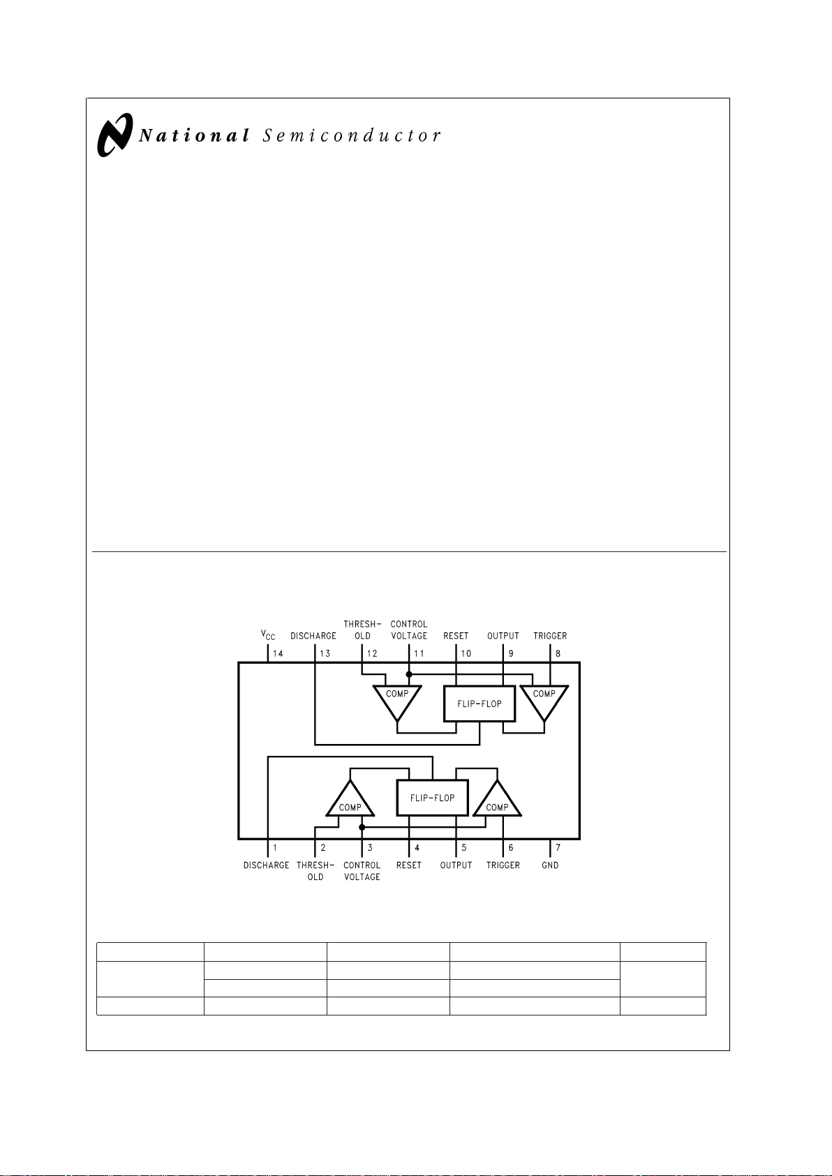
Connection Diagram
Ordering Information
Package Part Number Package Marking Media Transport NSC Drawing
14-Pin SOIC LM556CM LM556CM Rails
M14A
LM556CMX LM556CM 2.5k Units Tape and Reel
14-Pin MDIP LM556CN LM556CN Rails N14a
Dual-In-Line, Small Outline Packages
DS007852-1
Top View
March 2000
LM556 Dual Timer
© 2000 National Semiconductor Corporation DS007852 www.national.com
Page 2
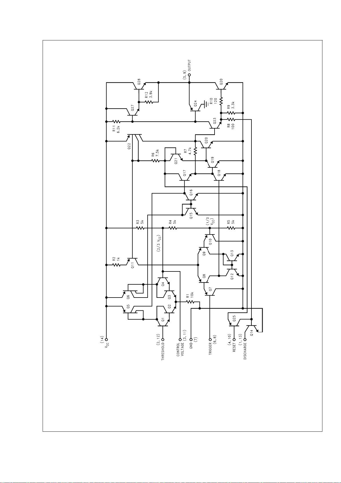
Schematic Diagram
DS007852-2
LM556
www.national.com 2
Page 3
Absolute Maximum Ratings (Note 1)
If Military/Aerospace specified devices are required,
please contact the National Semiconductor Sales Office/
Distributors for availability and specifications.
Supply Voltage +18V
Power Dissipation (Note 2)
LM556CM 410 mW
LM556CN 1620 mW
Operating Temperature Ranges
LM556C 0˚C to +70˚C
Storage Temperature Range −65˚C to +150˚C
Soldering Information
Dual-In-Line Package
Soldering (10 Seconds) 260˚C
Small Outline Packages
Vapor Phase (60 Seconds) 215˚C
Infrared (15 Seconds) 220˚C
See AN-450 “Surface Mounting Methods and Their Effect
on Product Reliability” for other methods of soldering
surface mount devices.
Electrical Characteristics
(TA= 25˚C, VCC= +5V to +15V, unless otherwise specified)
Parameter Conditions Limits Units
LM556C
Min Typ Max
Supply Voltage 4.5 16 V
Supply Current
(Each Timer Section)
V
CC
= 5V, RL=
∞
VCC= 15V, RL=
∞
(Low State) (Note 3)
3
10
6
14 mA
Timing Error, Monostable
Initial Accuracy 0.75 %
Drift with Temperature R
A
= 1k to 100kΩ, 50 ppm/˚C
C = 0.1µF, (Note 4)
Accuracy over Temperature 1.5 %
Drift with Supply 0.1 %/V
Timing Error, Astable
Initial Accuracy 2.25 %
Drift with Temperature R
A,RB
= 1k to 100kΩ, 150 ppm/˚C
Accuracy over Temperature C = 0.1µF, (Note 4) 3.0 %
Drift with Supply 0.30 %/V
Trigger Voltage V
CC
= 15V 4.5 5 5.5 V
V
CC
= 5V 1.25 1.67 2.0 V
Trigger Current 0.2 1.0 µA
Reset Voltage 0.4 0.5 1 V
Reset Current 0.1 0.6 mA
Threshold Current V
TH
= V-Control (Note 6)
V
TH
= 11.2V
0.03 0.1
250
µA
nA
Control Voltage Level and
Threshold Voltage
V
CC
= 15V
V
CC
=5V
9
2.6
10
3.33
11
4
V
Pin 1, 13
Leakage Output High
1 100 nA
Pin 1, 13 Sat (Note 7)
Output Low V
CC
= 15V, I = 15mA 180 300 mV
Output Low V
CC
= 4.5V, I = 4.5mA 80 200 mV
Output Voltage Drop (Low) V
CC
= 15V
I
SINK
= 10mA 0.1 0.25 V
I
SINK
= 50mA 0.4 0.75 V
I
SINK
= 100mA 2 2.75 V
I
SINK
= 200mA 2.5 V
V
CC
=5V
I
SINK
= 8mA V
I
SINK
= 5mA 0.25 0.35 V
LM556
www.national.com3
Page 4

Electrical Characteristics (Continued)
(TA= 25˚C, VCC= +5V to +15V, unless otherwise specified)
Parameter Conditions Limits Units
LM556C
Min Typ Max
Output Voltage Drop (High) I
SOURCE
= 200mA, VCC= 15V 12.5 V
I
SOURCE
= 100mA, VCC= 15V 12.75 13.3 V
V
CC
= 5V 2.75 3.3 V
Rise Time of Output 100 ns
Fall Time of Output 100 ns
Matching Characteristics (Note 8)
Initial Timing Accuracy 0.1 2.0 %
Timing Drift with Temperature
±
10 ppm/˚C
Drift with Supply Voltage 0.2 0.5 %/V
Note 1: Absolute Maximum Ratings indicate limits beyond which damage to the device may occur.
Note 2: For operating at elevated temperaturesthedevice must be derated based on a +150˚C maximum junction temperature and a thermal resistance of 77˚C/W
(Plastic Dip), and 110˚C/W (SO-14 Narrow).
Note 3: Supply current when output high typically 1mA less at V
CC
=5V.
Note 4: Tested at V
CC
= 5V and VCC= 15V.
Note 5: As reset voltage lowers, timing is inhibited and then the output goes low.
Note 6: This will determine the maximum value of R
A+RB
for 15V operation. The maximum total (RA+RB)is20MΩ.
Note 7: No protection against excessive pin 1, 13 current is necessary providing the package dissipation rating will not be exceeded.
Note 8: Matching characteristics refer to the difference between performance characteristics of each timer section.
Note 9: Refer to RETS556X drawing of military LM556J versions.
Typical Performance Characteristics
Minimum Pulse Width Required for Triggering
DS007852-3
Supply Current vs. Supply Voltage (Each Section)
DS007852-4
LM556
www.national.com 4
Page 5

Typical Performance Characteristics (Continued)
High Output Voltage vs. Output Source Current
DS007852-5
Low Output Voltage vs. Output Sink Current
DS007852-6
Low Output Voltage vs. Output Sink Current
DS007852-7
Low Output Voltage vs. Output Sink Current
DS007852-8
Output Propagation Delay vs. Voltage Level of Trigger
Pulse
DS007852-9
Output Propagation Delay vs. Voltage Level of Trigger
Pulse
DS007852-10
LM556
www.national.com5
Page 6

Typical Performance Characteristics (Continued)
Discharge Transistor (Pin 1, 13) Voltage vs. Sink
Current
DS007852-11
Discharge Transistor (Pin 1, 13) Voltage vs. Sink
Current
DS007852-12
LM556
www.national.com 6
Page 7

Physical Dimensions inches (millimeters) unless otherwise noted
Small Outline Package (M)
NS Package Number M14A
14-Lead (0.118” Wide) Molded Mini Small Outline Package
NS Package Number N14A
LM556
www.national.com7
Page 8

Notes
LIFE SUPPORT POLICY
NATIONAL’S PRODUCTS ARE NOT AUTHORIZED FOR USE AS CRITICAL COMPONENTS IN LIFE SUPPORT
DEVICES OR SYSTEMS WITHOUT THE EXPRESS WRITTEN APPROVAL OF THE PRESIDENT AND GENERAL
COUNSEL OF NATIONAL SEMICONDUCTOR CORPORATION. As used herein:
1. Life support devices or systems are devices or
systems which, (a) are intended for surgical implant
into the body, or (b) support or sustain life, and
whose failure to perform when properly used in
accordance with instructions for use provided in the
labeling, can be reasonably expected to result in a
significant injury to the user.
2. A critical component is any component of a life
support device or system whose failure to perform
can be reasonably expected to cause the failure of
the life support device or system, or to affect its
safety or effectiveness.
National Semiconductor
Corporation
Americas
Tel: 1-800-272-9959
Fax: 1-800-737-7018
Email: support@nsc.com
National Semiconductor
Europe
Fax: +49 (0) 180-530 85 86
Email: europe.support@nsc.com
Deutsch Tel: +49 (0) 69 9508 6208
English Tel: +44 (0) 870 24 0 2171
Français Tel: +33 (0) 1 41 91 8790
National Semiconductor
Asia Pacific Customer
Response Group
Tel: 65-2544466
Fax: 65-2504466
Email: ap.support@nsc.com
National Semiconductor
Japan Ltd.
Tel: 81-3-5639-7560
Fax: 81-3-5639-7507
www.national.com
LM556 Dual Timer
National does not assume any responsibility for use of any circuitry described, no circuit patent licenses are implied and National reserves the right at any time without notice to change said circuitry and specifications.
 Loading...