

Page 1
August 2006
LM5072
Integrated 100V Power Over Ethernet PD Interface and
PWM Controller with Aux Support
General Description
The LM5072 Powered Device (PD) interface and PulseWidth-Modulation (PWM) controller provides a complete
power solution, fully compliant to IEEE 802.3af, for the PD
connecting into Power over Ethernet (PoE) networks. This
controller integrates all functions necessary to implement
both a PD powered interface and DC-DC converter with a
minimum number of external components. The LM5072 provides the flexibility for the PD to also accept power from
auxiliary sources such as AC adapters in a variety of configurations. The low RDS(ON) PD interface hot swap MOSFET and programmable DC current limit extend the range of
LM5072 applications up to twice the power level of 802.3af
compliant PD devices. The 100V maximum voltage rating
simplifies selection of the transient voltage suppressor that
protects the PD from network transients. The LM5072 includes an easy-to-use PWM controller that facilitates the
various single-ended power supply topologies including the
flyback, forward and buck. The PWM control scheme is
based on peak current mode control, which provides inherent advantages including line feed-forward, cycle-by-cycle
current limit, and simplified feedback loop compensation.
Two versions of the LM5072 provide either an 80% maximum duty cycle (-80 suffix), or a 50% maximum duty cycle
(-50 suffix).
Features
PD Interface
n Fully Compliant IEEE 802.3af PD Interface
n Versatile Auxiliary Power Options
n 9V Minimum Auxiliary Power Operating Range
n 100V Maximum Input Voltage Rating
n Programmable DC Current Limit Up To 800mA
n 100V, 0.7Ω Hot Swap MOSFET
n Integrated PD Signature Resistor
n Integrated PoE Input UVLO
n Programmable Inrush Current Limit
n PD Classification Capability
n Power Good Indicator
n Thermal Shutdown Protection
PWM Controller
n Current Mode PWM Controller
n 100V Start-up Regulator
n Error Amplifier with 2% Voltage Reference
n Supports Isolated and Non-Isolated Applications
n Programmable Oscillator Frequency
n Programmable Soft-Start
n 800 mA Peak Gate Driver
n 80% Maximum Duty Cycle with Built-in Slope
Compensation (-80 device)
n 50% Maximum Duty Cycle, No Slope Compensation
(-50 device)
Applications
n IEEE 802.3af Compliant PoE Powered Devices
n Non-Compliant, Application Specific Devices
n Higher Power Ethernet Powered Devices
Packages
n TSSOP-16 EP (Exposed Pad)
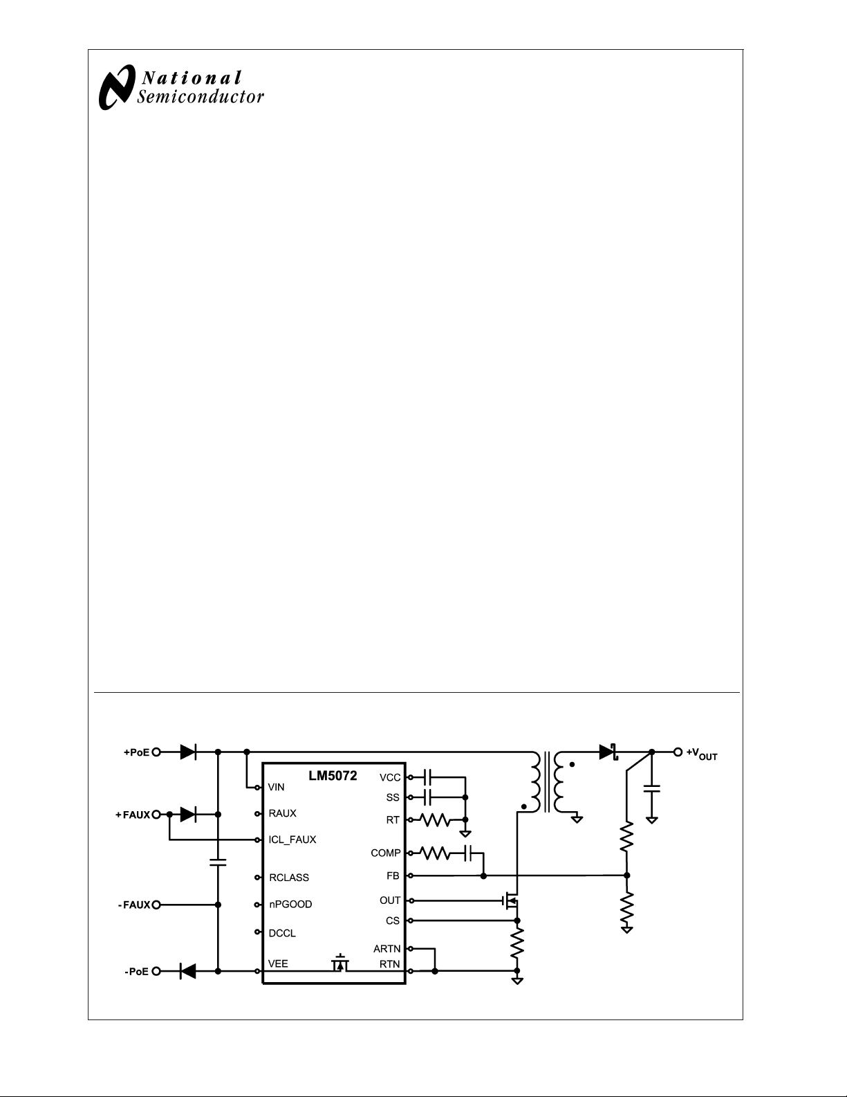
LM5072 Integrated 100V Power Over Ethernet PD Interface and PWM Controller with Aux Support
Simplified Application Diagram
20184601
© 2006 National Semiconductor Corporation DS201846 www.national.com
Page 2
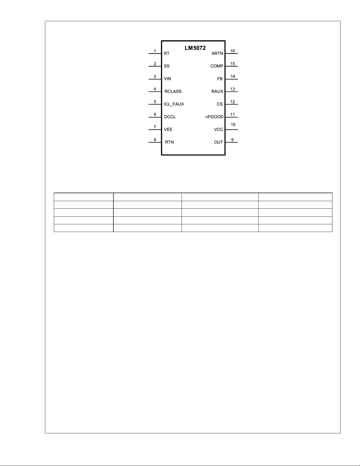
Connection Diagram
LM5072
16 Lead TSSOP-EP
20184602
Ordering Information
Order Number Description NSC Package Type / Drawing Supplied As
LM5072MH-50 50% Duty Cycle Limit TSSOP-16EP/MXA16A 92 units per rail
LM5072MHX-50 50% Duty Cycle Limit TSSOP-16EP/MXA16A 2500 units on tape and reel
LM5072MH-80 80% Duty Cycle Limit TSSOP-16EP/MXA16A 92 units per rail
LM5072MHX-80 80% Duty Cycle Limit TSSOP-16EP/MXA16A 2500 units on tape and reel
www.national.com 2
Page 3

Pin Descriptions
Pin Number Name Description
1 RT PWM controller oscillator frequency programming pin.
2 SS Soft-start programming pin.
3 VIN Positive supply pin for the PD interface and the internal PWM controller start-up regulator.
4 RCLASS PD classification programming pin.
5 ICL_FAUX Inrush current limit programming pin; also the front auxiliary power enable pin.
6 DCCL PD interface DC current limit programming pin.
7 VEE Negative supply pin for PD interface; connected to PoE and/or front auxiliary power return
path.
8 RTN PWM controller power return; connected to the drain of the internal PD interface hot swap
MOSFET; should be externally connected to the reference ground of the PWM controller.
9 OUT PWM controller gate driver output pin.
10 VCC PWM controller start-up regulator output pin.
11 nPGOOD PD interface Power Good indicator and delay timer pin; active low state indicates PoE
interface is in normal operation.
12 CS PWM controller current sense input pin.
13 RAUX Rear auxiliary power enable pin; can be programmed for auxiliary power dominance over
PoE power.
14 FB PWM controller voltage feedback pin and inverting input of the internal error amplifier;
connect to ARTN to disable the error amplifier in isolated dc-dc converter applications.
15 COMP Output of the internal error amplifier and control input to the PWM comparator. In isolated
applications, COMP is controlled by the secondary side error amplifier via an opto-coupler.
16 ARTN PWM controller reference ground pin; should be shorted externally to the RTN pin as a
single point ground connection to improve noise immunity.
EP Exposed metal pad on the underside of the device. It is recommended to connect this pad to
a PC Board plane connected to the VEE pin to improve heat dissipation.
LM5072
www.national.com3
Page 4
Absolute Maximum Ratings (Note 1)
If Military/Aerospace specified devices are required,
LM5072
please contact the National Semiconductor Sales Office/
Distributors for availability and specifications.
VIN , RTN to VEE (Note 7) -0.3V to 100V
RAUX to ARTN -0.3V to 100V
ICL_FAUX to VEE -0.3V to 100V
DCCL, RCLASS to VEE -0.3V to 7V
nPGOOD to ARTN -0.3V to 16V
ARTN to RTN -0.3V to 0.3V
VCC, OUT to ARTN -0.3V to 16V
CS, FB, RT to ARTN -0.3V to 7V
COMP, SS to ARTN -0.3V to 5.5V
ESD Rating
Human Body Model (Note 2) 2000V
Lead Soldering Temp. (Note 3)
Wave (4 seconds)
Infrared (10 seconds)
Vapor Phase (75 seconds)
260˚C
240˚C
219˚C
Storage Temperature -55˚C to 150˚C
Junction Temperature 150˚C
Operating Ratings
VINvoltage 9V to 70V
External voltage applied to V
CC
Operating Junction Temperature -40˚C to 125˚C
8V to 15V
Electrical Characteristics (Note 4) Specifications in standard type face are for T
boldface type apply over the full operating junction temperature range. Unless otherwise specified: V
= +25˚C and those in
J
= 48V, F
IN
OSC
=
250kHz.
SYMBOL PARAMETER CONDITIONS MIN TYP MAX UNITS
Detection and Classification
V
Signature Startup Voltage 1.5 V
IN
Signature Resistance 23.25 24.5 26 kΩ
Signature Resistor Disengage/
V
Rising 11.0 12.0 12.6 V
IN
Classification Engage
Hysteresis 1.9 V
Classification Current Turn Off V
Rising 22 23.5 25 V
IN
Classification Voltage 1.213 1.25 1.287 V
Supply Current During Classification V
= 17V 0.7 1.1 mA
IN
Line Under Voltage Lock-Out
UVLO Release V
UVLO Lock out V
Rising 36 38.5 40 V
IN
Falling 29.5 31.0 32.5 V
IN
UVLO Hysteresis 6 V
UVLO Filter 300 µs
Power Good
VDS Required for Power Good Status 1.3 1.5 1.7 V
VDS Hysteresis of Power Good Status 0.8 1.0 1.2 V
VGS Required for Power Good Status 4.5 5.5 6.5 V
Default Delay Time of Loss-of Power
30 µs
Good Status
nPGOOD current Source 45 55 65 µA
nPGOOD Pull Down Resistance 130 250 Ω
nPGOOD Threshold 2.3 2.5 2.7 V
Hot Swap
RDS(ON) Hot Swap MOSFET Resistance 0.7 1.2 Ω
Hot Swap MOSFET Leakage 110 µA
Default Inrush Current Limit V
Default DC Current Limit V
Front Auxiliary DC Current Limit V
Inrush Current Limit Programming
= 4.0V 120 150 180 mA
DS
= 4.0V 380 440 510 mA
DS
= 4.0V 470 540 610 mA
DS
V
= 4.0V -15 15 %
DS
Accuracy
DC Current Limit Programming Accuracy VDS= 4.0V -12 12 %
www.national.com 4
Page 5
LM5072
Electrical Characteristics (Note 4) Specifications in standard type face are for T
boldface type apply over the full operating junction temperature range. Unless otherwise specified: V
= +25˚C and those in
J
= 48V, F
IN
OSC
=
250kHz. (Continued)
SYMBOL PARAMETER CONDITIONS MIN TYP MAX UNITS
Auxiliary Power Option
ICL_FAUX Threshold ICL_FAUX Pin Rising 8.1 8.7 9.3 V
ICL_FAUX Pull Down Current 50 µA
RAUX Lower Threshold (I = 22 µA) RAUX Pin Rising 2.3 2.5 3.0 V
RAUX Lower Threshold Hysteresis 0.8 V
RAUX Upper Threshold (I = 250 µA) RAUX Pin Rising 5.4 6.0 6.9 V
RAUX Lower Threshold Current 16 22 28 µA
RAUX Upper Threshold Current 187 250 313 µA
VCC Regulator
VccReg VCC Regulation (VccReg) 7.4 7.7 8 V
VCC Current Limit 15 mA
VCC UVLO (Rising) VccReg
– 210
mV
VccReg
– 100
mV
VCC UVLO (Falling) 5.9 6.2 6.5 V
VIN Supply Current V
Supply Current (Icc) V
VCC Regulator Dropout V
= 10V 2.0 mA
CC
= 10V 3 mA
CC
IN–VCC
(Note 6) 6.5 V
Error Amplifier
Gain Bandwidth 3 MHz
DC Gain 67 dB
Input Voltage 1.225 1.275 V
COMP Sink Capability 5 10 mA
Current Limit
ILIM Delay to Output 30 ns
Cycle by Cycle Current Limit Threshold
0.45 0.5 0.55 V
Voltage
Leading Edge Blanking Time 65 ns
CS Sink Impedance (clocked) 35 55 Ω
Soft-start
Soft-start Current Source 8 10 12 µA
Oscillator
Frequency1 (R
Frequency2 (R
= 26.1 kΩ) 175 200 225 KHz
T
= 8.7 kΩ) 515 580 645 KHz
T
Sync threshold 2.6 3.2 3.8 V
PWM Comparator
Delay to Output 25 ns
Min Duty Cycle 0 %
Max Duty Cycle (-80 Device) 75 80 85 %
Max Duty Cycle (-50 Device) 47 50 53 %
COMP to PWM Comparator Gain 0.33
COMP Open Circuit Voltage 4.3 5.2 6.1 V
COMP Short Circuit Current 0.6 1.0 1.4 mA
Slope Compensation (LM5072-80 Device Only)
Slope Comp Amplitude 70 90 110 mV
Output Section
Output High Saturation 0.25 0.75 V
mV
www.national.com5
Page 6
Electrical Characteristics (Note 4) Specifications in standard type face are for T
boldface type apply over the full operating junction temperature range. Unless otherwise specified: V
LM5072
250kHz. (Continued)
= +25˚C and those in
J
= 48V, F
IN
SYMBOL PARAMETER CONDITIONS MIN TYP MAX UNITS
Output Low Saturation 0.25 0.75 V
t
r
t
f
Rise time C
Fall time C
= 1nF 18 ns
LOAD
= 1nF 15 ns
LOAD
PDI Thermal Shutdown (Note 5)
Thermal Shutdown Temp. 165 ˚C
Thermal Shutdown Hysteresis 25 ˚C
Thermal Resistance
θ
JA
Note 1: Absolute Maximum Ratings are limits beyond which damage to the device may occur. Operating Ratings are conditions under which operation of the device
is intended to be functional. For guaranteed specifications and test conditions, see the Electrical Characteristics.
Note 2: The human body model is a 100 pF capacitor discharged through a 1.5 kΩ resistor into each pin.
Note 3: For detailed information on soldering the plastic TSSOP package, refer to the Packaging Databook available from National Semiconductor.
Note 4: Minimum and Maximum limits are guaranteed through test, design, or statistical correlation using Statistical Quality Control (SQC) methods. Typical values
represent the most likely parametric norm at T
Level (AOQL).
Note 5: Device thermal limitations may limit usable range.
Note 6: The VCC regulator is intended for use solely as a bias supply for the LM5072, dropout assumes 3mA of external V
Note 7: During rear auxiliary operation, the RTN pin can be approximately -0.4V with respect to VEE. This is caused by normal internal bias currents, and will not
harm the device. Application of external voltage or current must not cause the absolute maximum rating to be exceeded.
Junction to Ambient MXA package 40 ˚C/W
= 25˚C, and are provided for reference purpose only. Limits are used to calculate National’s Average Outgoing Quality
J
current.
CC
OSC
=
www.national.com 6
Page 7
Typical Performance Characteristics
UVLO Threshold vs Temperature Default Current Limit vs Temperature
LM5072
20184603
20184604
Inrush Current Limit vs ICL_FAUX Resistor DC Current Limit vs. DCCL Resistor
20184605 20184606
Programmed DC Current Limit vs Temperature Oscillator Frequency vs Temperature
20184607
20184608
www.national.com7
Page 8
Typical Performance Characteristics (Continued)
LM5072
Oscillator Frequency vs RT Resistance Error Amplifier Reference Voltage vs Temperature
20184610
VCCvs I
20184609
CC
Input Current vs Input Voltage
20184611
Maximum Duty Cycle vs Temperature Soft-start Current vs Temperature
20184613
www.national.com 8
20184612
20184614
Page 9

Specialized Block Diagrams
LM5072
FIGURE 1. Top Level Block Diagram
20184615
www.national.com9
Page 10

Specialized Block Diagrams (Continued)
LM5072
FIGURE 2. PWM Controller Block Diagram
Description of Operation and Applications Information
The LM5072 integrates a fully IEEE 802.3af compliant PD
interface and PWM controller in a single integrated circuit,
providing a complete and low cost power solution for devices
that connect to PoE systems. The implementation requires a
minimal number of external components.
The LM5072’s Hot Swap PD interface provides four major
advantages:
1. An input voltage rating up to 100V that allows greater
flexibility when selecting a transient surge suppressor to
protect the PD from voltage transients encountered in
PoE applications.
2. The integration of the PD signature resistor and other
functions including programmable inrush current limit,
input voltage under-voltage lock-out (UVLO), PD classification, and thermal shutdown simplifies PD implementation.
3. The PD interface and PWM controller accept power from
auxiliary sources including AC adapters and solar cells
in various configurations and over a wide range of input
voltages. Auxiliary power input can be programmed to
be dominant over PoE power.
20184616
4. DC current limit is programmable and adjustable to support PoE applications requiring input currents up to 700
mA.
The LM5072 includes an easy to use PWM controller based
on the peak current mode control technique. Current mode
control provides inherent advantages such as line voltage
feed-forward, cycle-by-cycle current limit, and simplified
closed-loop compensation. The controller’s PWM gate driver
is capable of sourcing and sinking peak currents of 800 mA
to directly drive the power MOSFET switch of the DC-DC
converter. The PWM controller also contains a high gain,
high bandwidth error amplifier, a high voltage startup bias
regulator, a programmable oscillator for a switching frequency between 50 kHz to 500 kHz, a bias supply (V
under-voltage lock-out circuit, and a programmable soft-start
circuit. These features greatly simplify the design and implementation of single ended topologies like the flyback, forward and buck.
The LM5072 is available in two versions, the LM5072-50 and
LM5072-80. As indicated in the suffix of the part number, the
maximum duty cycle of each device is limited to 50% and
80%, respectively. Internal PWM controller slope compensation is provided in the LM5072-80 version.
CC
)
www.national.com 10
Page 11

Modes of Operation
Per the IEEE 802.3af specification, when a PD is connected
to a PoE system it transitions through several operating
modes in sequence including detection, classification (optional), turn on, normal operation, and power removal. Each
operating mode corresponds to a specific PoE voltage range
fed through the Ethernet cable. Figure 3 shows the IEEE
802.3af specified sequence of operating modes and the
corresponding PD input voltages.
Current steering diode-bridges are required for the PD interface to accept all allowable connections and polarities of
LM5072
PoE voltage from the RJ-45 connector (see the example
application circuits in Figures 18, 19, 20 and 21). The bridge
will cause some reduction of the input voltage sensed by the
LM5072. To guarantee full compliance to the specification in
all operating modes, the LM5072 takes into account the
voltage drop across the bridge diodes and responds appropriately to the voltage received from the PoE cable. Table 1
presents the response in each operating mode to voltages
across the VIN and VEE pins.
20184617
FIGURE 3. Sequence of PoE Operating Modes
TABLE 1. Operating Modes With Respect To Input Voltage
Mode of Operation
Voltage from PoE Cable per
IEEE 802.3af
LM5072 Input Voltage
(VINpin to VEEpin)
Detection (Signature) 2.7V to 10.0V 1.5V to 10.0V
Classification 14.5V to 20.5V 12V to 23.5V
Startup 42V max 38V (UVLO Release, V
Normal Operation 57V to 36V 70V to 32V (UVLO, V
IN
Falling)
IN
Rising)
www.national.com11
Page 12

Detection Signature
During detection mode, a PD must present a signature re-
LM5072
sistance between 23.75 kΩ and 26.25 kΩ to the PoE power
sourcing equipment. This signature impedance distinguishes
the PD from non-PoE capable equipment to protect the latter
from being accidentally damaged by inadvertent application
of PoE voltage levels. To simplify the circuit implementation,
the LM5072 integrates the 24.5 kΩ signature resistor, as
shown in Figure 4.
FIGURE 4. Detection Circuit With Integrated PD
Signature Resistor
TABLE 2. Classification Levels and Required External Resistor Value
PD Max Power Level ICLASS Range
Class
0 (Default) 0.44W 12.95W 0 mA 4 mA Open
1 0.44W 3.84W 9 mA 12 mA 130Ω
2 3.84W 6.49W 17 mA 20 mA 71.5Ω
3 6.49W 12.95W 26 mA 30 mA 46.4Ω
4 Reserved Reserved 36 mA 44 mA 31.6Ω
During detection mode, the voltage across the VIN and VEE
pins is less than 10V. Once signature mode is complete, the
LM5072 will disengage the signature resistor to reduce
power loss in all other modes.
Classification
Classification is an optional feature of the IEEE802.3af
specification. It is primarily used to identify the power requirements of a particular PD device. This feature will allow
the PSE to allocate the appropriate available power to each
device on the network. Classification is performed by measuring the current flowing into the PD during this mode. IEEE
802.3af specifies five power classes, each corresponding to
a unique range of classification current, as presented in
Table 2. The LM5072 simplifies the classification implementation by requiring a single external resistor connected between the RCLASS and VEE pins to program the classification current. The resistor value required for each class is also
given in Table 2.
20184618
LM5072
RCLASS ValueFrom To From To
FIGURE 5. PD Classification – Fulfilled With a Single External Resistor
Figure 5 shows the LM5072’s implementation of PD classification using an external resistor connected to the RCLASS
pin. During classification, the voltage across the VIN and
VEE pins is between 13V and 23.5V. In this voltage range,
the class resistor RCLASS is engaged by enabling the 1.25V
buffer amplifier and MOSFET. After classification is complete, the voltage from the PSE will increase to the normal
www.national.com 12
20184619
operating voltage of the PoE system (48V nominal). When
rises above 23.5V, the LM5072 will disengage the
V
IN
RCLASS resistor to reduce on-chip power dissipation.
The classification feature is disabled when either the front or
rear auxiliary power options are selected, as the classification function is not required when power is supplied from an
auxiliary source. The classification function is also disabled
when the LM5072 reaches the thermal shutdown temperature threshold (nominally 165˚C). This may occur if the
Page 13

LM5072
Classification (Continued)
LM5072 is operated at elevated ambient temperatures and
the classification time exceeds the IEEE802.3af limit of 75
ms.
When the classification option is not required, simply leave
the RCLASS pin open to set the PD to the default Class 0
state. Class 0 requires that the PSE allocate the maximum
IEEE802.3af specified power of 15.4 W (12.95 W at the PD
input terminals) to the PD.
Undervoltage Lockout (UVLO)
The LM5072’s internal preset UVLO circuit continuously
monitors the PoE input voltage between the VIN and VEE
pins. When the V
UVLO circuit will release the hot swap MOSFET and initiate
the startup inrush sequence. When the V
below 31V nominal during normal operating mode, the
LM5072 disables the PD by shutting off the hot swap
MOSFET.
voltage rises above 38V nominal, the
IN
voltage falls
IN
FIGURE 6. Preset Input UVLO Function
Figure 6 illustrates the block diagram of the LM5072 UVLO
circuit. This function requires no external components. The
UVLO signal can be over-ridden by the front auxiliary power
option (see details in the FAUX section) to allow the hot
swap MOSFET of the LM5072 to pass power from front
auxiliary power sources at voltage levels below the PoE
operating voltage. In the rear auxiliary power application
(see RAUX section), the auxiliary power source bypasses
the hot swap MOSFET and is applied directly to the input of
the DC-DC converter. The UVLO function does not need to
be over-ridden in this configuration.
The PD can draw a maximum current of 400 mA during
standard 802.3af PoE operation. This current will cause a
voltage drop of up to 8V over a 100m long Ethernet cable.
The PD front-end current steering diode bridges may introduce an additional 2V drop. In order to guarantee successful
startup at the minimum PoE voltage of 42V, and to continue
operation at the minimum requirement of 36V as specified by
IEEE 802.3af, these voltage drops must be taken into account. Therefore, the LM5072 UVLO thresholds have been
set to 38V on the rising edge of VIN, and 31V on the falling
20184620
edge of VIN. The 7V nominal hysteresis of the UVLO function, in addition to the inrush current limit (discussed in the
next section), prevents false starts and chattering during
startup.
Inrush Current Limit Programming
According to IEEE 802.3af, the input capacitance of the PD
power supply must be at least 5 µF (between the VIN and
RTN pins). Considering the capacitor tolerance and the effects of voltage and temperature, a nominal capacitor value
of at least 10 µF is recommended to ensure 5 µF minimum
under all conditions. A greater amount of capacitance may
be needed to filter the input ripple of the DC-DC converter.
The input capacitors remain discharged during detection and
classification modes of the PD interface. The hot swap MOSFET is turned on after the VIN minus VEE voltage difference
rises above the UVLO release threshold of 38V nominal.
When enabled, the hot swap MOSFET delivers a regulated
inrush current to charge the input capacitors of the DC-DC
converter. To prevent excessive inrush current, the LM5072
www.national.com13
Page 14

Inrush Current Limit Programming
(Continued)
LM5072
will turn on the hot swap MOSFET in a constant current
mode. The default, pre-programmed inrush current of 150
mA can be selected by simply leaving the ICL_FAUX pin
open.
To adjust the capacitor charging time for a particular application requirement, the inrush limit can be programmed to
any value between 150 and 400 mA with an external resistor
) between the ICL_FAUX and VEE pins, as shown in
(R
ICL
Figure 7. The relationship between the R
desired inrush current limit I
INRUSH
equation:
ICL
satisfies the following
value and the
20184624
FIGURE 8. Input DC Current Limit Programming via
R
DCCL
The maximum recommended DC current limit is 800 mA.
While thermal analysis should be a standard part of the
module development process, it may warrant additional attention if the DC current limit is programmed to values in
excess of 400 mA. This analysis should include evaluations
of the dissipation capability of LM5072 package, heat sinking
properties of the PC Board, ambient temperature, and other
heat dissipation factors of the operating environment.
20184622
FIGURE 7. Input Inrush Limit Programming via R
ICL
The inrush current causes a voltage drop along the PoE
Ethernet cable (20Ω maximum) that reduces the input voltage sensed by the LM5072. To avoid erratic turn-on (hiccups), I
should be programmed such that the input
INRUSH
voltage drop due to cable resistance does not exceed the
V
hysteresis (6V minimum).
IN-UVLO
DC Current Limit Programming
The LM5072 provides a default DC current limit of 440 mA
nominal. This default limit can be selected by leaving the
DCCL pin open.
The LM5072 allows the DC current limit to be programmed
within the range from 150 mA to 800 mA. Figure 8 shows the
method to program the DC current limit with an external
resistor, R
. The relationship between the R
DCCL
and the desired DC current limit I
equation:
satisfies the following
DC
DCCL
value
Power Good and Regulator Startup
The Power Good status indicates that the circuit is ready for
PWM controller startup to occur. It is established when the
input capacitors are fully charged through the hot swap
MOSFET. Since the hot swap MOSFET is in series with the
input capacitors of the DC-DC converter, its drain-to-source
voltage decreases as the charging occurs. Power Good is
indicated when the following two conditions are met: the
MOSFET drain-to-source voltage drops below 1.5V (with 1V
hysteresis), and the gate-to-source voltage is greater than
5V. Circuitry internal to the LM5072 monitors both the drain
and gate voltages (see Figure 1), and issues the Power
Good status flag by pulling down the nPGOOD pin to a logic
low level relative to the ARTN pin.
The nPGOOD circuitry consists of a 2.5V comparator, a
130Ω pull down MOSFET, and a 50 µA pull up current
source, as shown in Figure 9. Once the Power Good status
is established, the nPGOOD pin voltage will be pulled down
quickly by the MOSFET, and the PWM controller will start as
soon as the nPGOOD pin voltage drops below the 2.5V
threshold.
www.national.com 14
Page 15

Power Good and Regulator Startup (Continued)
FIGURE 9. "Powered-from-PoE" Indictor and Power Good Delay Timer
LM5072
20184625
The nPGOOD pin can be configured to perform multiple
functions. As shown in Figure 9, it can be used to implement
a “Powered from PoE” indicator using an LED with a series
current limiting resistor connected to the VCC pin. This may
be useful when the auxiliary power source is directly connected to the DC-DC converter stage, a situation known as
“RAUX” (see Auxiliary Power Options below). In such a
configuration, the nPGOOD pin will be active when the PD is
operating from PoE power but not when it is powered from
the auxiliary source. However, the “Powered from PoE” indicator is not applicable in systems implementing the front
auxiliary power configuration “FAUX” (see Auxiliary Power
Options below) because both PoE and auxiliary supply current pass through the hot swap MOSFET. In this configuration, the nPGOOD pin is active when either PoE power or
auxiliary power is applied. The designer should ensure that
the current drawn by the LED is not more than a few milliamps, as the V
regulator’s output current is limited to 15
CC
mA and must also supply the LM5072’s bias current and
external MOSFET’s gate charging current. Supplying an
external V
that is higher than the regulated level with a
CC
bench supply is an easy way to measure VCC load during
normal operation. It should also be noted that an external
load on the V
regulator. This may be a concern when operating from a
V
CC
line will increase the dropout voltage of the
CC
low voltage rear auxiliary supply.
The nPGOOD pin can also be used to implement a delay
timer by adding a capacitor from the nPGOOD pin to the
ARTN pin. This delay timer will prevent the interruption of the
PWM controller’s operation in the event of an intermittent
loss of Power Good status. This can be caused by PoE line
voltage transients that may occur when switching between
normal PoE power and a backup supply system (e.g. a
battery or UPS). This condition will create a new “hot swap”
event if there is a voltage difference between the backup
supply and PoE supply. Since the hot swap MOSFET will
likely limit current during such a sudden input voltage
change, the nPGOOD pin will momentarily switch to the ”pull
up” state. A capacitor on this pin will delay the transition of
the nPGOOD pin state in order to provide continuous opera-
tion of the PWM controller during such transients. The Power
Good filter delay time and capacitor value can be selected
with the following equation:
For example, selecting 1000 nF for C
, the delay time
PGOOD
will be 50 ms if no LED is used and about 0.83 ms when an
LED, drawing 3 mA, is used. The delay required for continued operation will depend on the amplitude of the transient,
the DC current limit, the load, and the total amount of input
capacitance. Note that this delay does not guarantee continued operation. If the hot swap MOSFET is in current limit for
an extended period, it may cause a thermal limit condition.
This will result in a complete shutdown of the switching
regulator, though no elements in the system will be permanently damaged and normal operation will resume momentarily.
The Power Good status will also affect the default DC current limit. Should the sensed drain to source voltage of the
hot swap MOSFET (from ARTN to V
) exceed 2.5V, the
EE
LM5072 will increase the DC current limit from the default
440 mA to 540 mA, thus allowing the PD to continue operation through the transient event. This higher current limit will
remain in effect until one of the following events occur: (i) the
duration of loss of Power Good status exceeds t
PG_Delay
,at
which time the PWM controller will be disabled, (ii) the
increased power dissipation in the hot swap MOSFET
causes a thermal limit condition as previously discussed, or
(iii) the MOSFET drain to source voltage falls below 1.5V to
re-establish Power Good status. Under this condition, the
LM5072 will revert back to the default 440 mA DC current
limit once Power Good status is restored. Note that if the DC
current limit has been programmed externally with R
DCCL
(see the DC current limit section), the DC current limit will
remain at the programmed level even when the Power Good
status is lost.
www.national.com15
Page 16

Auxiliary Power Options
The LM5072 based PD can receive power from auxiliary
LM5072
sources like AC adapters and solar cells in addition to the
PoE enabled network. This is a desirable feature when the
total system power requirements exceed the PSE’s load
capacity. Furthermore, with the auxiliary power option the PD
can be used in a standard Ethernet (non-PoE) system.
For maximum versatility, the LM5072 accepts two different
auxiliary power configurations. The first one, shown in Figure
10, is the front auxiliary (FAUX) configuration in which the
auxiliary source is “diode OR’d” with the PoE potential received from the Ethernet connector. The second configuration, shown in Figure 11, is the rear auxiliary (RAUX) option
in which the auxiliary power bypasses the PoE interface and
is connected directly to the input of the DC-DC converter
through a diode. The FAUX option is desirable if the auxiliary
power voltage is similar to the PoE input voltage. However,
when the auxiliary supply voltage is much lower than the
PoE input voltage, the RAUX option is more favorable because the current from the auxiliary supply is not limited by
the hot swap MOSFET DC current limit. A comparison of the
FAUX and RAUX options is presented in Table 3. Note the
ICL_FAUX and RAUX pins are not reverse voltage protected. If complete reverse protection is desired, series
blocking diodes are necessary.
FIGURE 10. The FAUX Configuration
20184627
20184628
FIGURE 11. The RAUX Configuration
www.national.com 16
Page 17

Auxiliary Power Options (Continued)
TABLE 3. Comparison Between FAUX and RAUX Operation
Tradeoff FAUX Operation RAUX Operation
Hot Swap Protection / Current Limit
Protection
Minimum Auxiliary Voltage
(at the IC pins)
Auxiliary Dominance Over PoE Cannot be forced without external
Use of nPGOOD Pin as “Powered
from PoE” Indicator
Transient Protection Excellent due to active MOSFET
Automatically provided by the hot
swap MOSFET.
Limited to 18V by the signature
detection mode, or by the power
requirement (current limit).
components.
Not applicable as power is delivered
through the hot swap interface in both
PoE and FAUX modes.
current limit.
LM5072
Requires a series resistor to limit the inrush
current during hot swap.
Only limited by 9V minimum input requirement.
Can be forced with appropriate RAUX pin
configuration.
Supported.
Fair due to passive resistor current limit.
The term “Auxiliary Dominance” mentioned in Table 3 means
that when the auxiliary power source is connected, it will
always power the PD regardless of the state of PoE power.
“Aux dominance” is achievable only with the RAUX option,
as noted in the table.
If the PD is not designed for aux dominance, either the FAUX
or RAUX power sources will deliver power to the PD only
under the following two conditions: (i) If auxiliary power is
applied before PoE power, it will prevent the PD’s detection
by the PSE and will supply power indefinitely. This occurs
because the PoE input bridge rectifiers will be reverse biased, so no detection signature will be observed. Under this
condition, when the auxiliary supply is removed, power will
not be maintained because it will take some time for the PSE
to perform signature detection and classification before it will
supply power. (ii) If auxiliary power is applied after PoE
power is already present but has a higher voltage than PoE,
it may assume power delivery responsibility. Under the second case, if the supplied voltages are comparable, the load
current may be shared inversely proportional to the respective output impedances of each supply. (The output impedance of the PSE supply is increased by the cable series
resistance).
If PoE power is applied first and has a higher voltage than
the non-dominant aux power source, it will continue powering the PD even when the aux power source becomes
available. In this case, should PoE power be removed, the
auxiliary source will assume power delivery and supply the
DC-DC loads without interruption.
If either FAUX or RAUX power is supplied prior to PoE
power, it will prevent the recognition of the PD by the PSE.
Consequently, continuity of power delivery cannot be guaranteed because the PoE supply will not be present when
auxiliary power is removed.
Pulling up the ICL_FAUX pin will increase the default DC
current limit to 540 mA. This increase in DC current limit is
necessary because higher current is required to support the
PD output power at the lower input potentials observed with
auxiliary sources. In cases where the auxiliary supply voltage is comparable to the PoE voltage, there is no need to
pull-up the ICL_FAUX pin to override VIN UVLO, and the
default DC current limit remains at 440 mA. However, if the
DC current limit is externally programmed with R
condition of the ICL_FAUX pin will not affect the programmed DC current limit. In other words, programmed DC
current limit can be considered a “hard limit” that will not vary
in any configuration.
DCCL
, the
RAUX Option
The RAUX option is desirable when the auxiliary supply
voltage is significantly lower than the PoE voltage or when
aux dominance is desired. The inrush and DC current limits
of the LM5072 do not protect or limit the RAUX power
source, and an additional resistor in the RAUX input path will
be needed to provide transient protection.
To select the RAUX option without aux dominance, simply
pull up the RAUX pin to the auxiliary power supply voltage
through a high value resistor. Depending on the auxiliary
supply voltage, the resistor value should be selected such
that the current flowing into the RAUX pin is approximately
100 µA when the pin is mid-way between the lower and
upper RAUX thresholds (approximately 4V). For example,
with an 18V non-dominant rear auxiliary supply, the pull up
resistor should be:
FAUX Option
With the FAUX option, the LM5072 hot swap MOSFET provides inrush and DC current limit protection for the auxiliary
power source. To select the FAUX configuration for an auxiliary voltage lower than nominal PoE voltages, the
ICL_FAUX pin must be forced above its high threshold to
override the VIN UVLO function. Note that when the
ICL_FAUX pin is pulled high to override VIN UVLO, it also
overrides the inrush current limit programmed by R
present. In this case, the inrush current will revert back to the
default 150 mA limit.
ICL
,if
If the PSE load capacity is limited and insufficient, aux
dominance will be a desired feature to off load PoE power for
other PDs that do not have auxiliary power available. Aux
dominance is achieved by pulling the RAUX pin up to the
auxiliary supply voltage through a lower value (~5kΩ) resis-
tor that delivers at least 250 µA into the RAUX pin. When this
higher RAUX current level is detected, the LM5072 shuts
down the PD interface. In aux dominant mode, the auxiliary
power source will supply the PD system as soon as it is
applied. PD operation will not be interrupted when the aux
power source is connected. The PoE source may or may not
www.national.com17
Page 18

RAUX Option (Continued)
actually be removed by the PSE, although the DC current
LM5072
from the network cable is effectively reduced to zero (
µA). IEEE 802.3af requires the AC input impedance to be
greater than 2 MΩ to ensure PoE power removal. This
condition is not satisfied when the auxiliary power source is
applied. The PSE may remove power from a port based on
the reduction in DC current. This is commonly known as DC
Maintain Power Signature (DC MPS), a common feature in
many PSE systems.
The high voltage startup regulator of the PWM controller
does not have low dropout capability and will not be able to
provide V
14.5V (no external V
voltage should supply V
when the potential from VIN to RTN is less than
CC
load). In this case, the auxiliary
CC
directly via diode OR-ing to en-
CC
sure successful startup.
When using the RAUX configuration, the positive potential
connection of the 0.1 µF signature capacitor should be
moved from VIN to RTN/ARTN as shown in Figure 11. This
provides a high frequency, low impedance path for the IC’s
substrate during rear auxiliary operation. Placing the capacitor here will not affect signature mode.
It should be noted that rear auxiliary non-dominance does
not imply PoE dominance. PoE dominance is difficult to
achieve in any PoE system if continuity of power is desired.
When the PoE voltage appears, the PSE and PD interface
must continue delivering load current in addition to charging
the input capacitor bank from the auxiliary voltage to the PoE
voltage. The situation is further complicated by the fact that
for a given delivered power level, the load current is much
higher at the lower input voltages typically used in auxiliary
supplies. As is the case during any inrush sequence, very
high power is dissipated in the hot swap MOSFET. Consequently, attempting to achieve inrush completion while delivering load current is highly ill advised. Lastly, current delivered to the system may be limited by the PSE, the PD, or
both.
A Note About FAUX and RAUX Pin False Input State Detection
The ICL_FAUX and RAUX pins are used to sense the presence of auxiliary power sources. The input voltage of each
pin must remain low when the auxiliary power sources are
absent. However, the Or-ing diodes feeding the auxiliary
power are not ideal and leak reverse current that can flow
from the PoE input to both the ICL_FAUX and RAUX pins.
When PoE power is applied, these leakage currents may
elevate the potentials of the ICL_FAUX and RAUX pins to
false logic states.
One of two failure modes may be observed when the power
diode feeding the front auxiliary input leaks excessively.
First, the current may corrupt the inrush current limit programming, if that feature has been implemented. Second,
the leakage current may elevate the voltage on the pin to the
ICL_FAUX input threshold, which will force UVLO release.
This would certainly interrupt any attempt by the LM5072 PD
interface to perform the signature or classification functions.
When the power diode that feeds the rear auxiliary input
leaks, the false signal could imply a rear auxiliary supply is
present. In this case, the internal hot swap MOSFET will be
turned off. This would of course block PoE power flow and
cause the circuit to prevent startup.
This leakage problem at the control input pins can be easily
solved. As shown in Figure 12, an additional pull-down re-
sistor (Rpd) across each auxiliary power control input provides a path for the diode leakage current so that it will not
create false states on the ICL_FAUX or RAUX pins.
<
150
20184629
FIGURE 12. Bypassing Resistor – Prevents False
ICL_FAUX and RAUX Pin Signaling
High Voltage Startup Regulator
The LM5072 contains a startup bias regulator that allows the
VIN pin to be connected directly to PoE network voltages as
high as 100V. The regulator output is connected to the VCC
pin, providing an initial DC bias voltage of 7.7V nominal to
start the PWM controller. The regulator is internally current
limited to no less than 15 mA to prevent excessive power
dissipation. For V
voltage stability and noise immunity, a
CC
capacitor ranging between 0.1 µF to 10 µF is required between the VCC and ARTN pins. Though the current capability of the regulator exceeds the requirements of the IC, no
external DC load drawing more than 3 mA should be applied
to the output. A small amount of current for a “Powered from
PoE” indicator LED (see Power Good section) is acceptable.
After the DC-DC converter reaches steady state operation,
the V
of the power transformer. The sustained V
voltage is typically elevated by an auxiliary winding
CC
voltage should
CC
be greater than 8.1V to guarantee the current supplied by
the startup regulator is reduced to zero. Increasing the VCC
pin voltage above the regulation level of the startup regulator
automatically disables the regulator, thus reducing the power
dissipation inside the LM5072. The power savings can be
significant as many high voltage MOSFETs require a relatively large amount of gate charge and the gate drive current
adds directly to the V
under-voltage lock-out circuit monitors the VCCvolt-
AV
CC
age to prevent the PWM controller from operating as the V
current draw.
CC
CC
voltage rises during startup or falls during shutdown. The
PWM controller is enabled when the V
exceeds 7.6V and disabled when the V
voltage rising edge
CC
voltage falling
CC
edge drops below 6.25V.
Error Amplifier
The LM5072 contains a wide-bandwidth, high-gain error amplifier to regulate the output voltage in non-isolated applications. The amplifier’s non-inverting input is set to a fixed
reference voltage of 1.25V, while the inverting input is connected to the FB pin. The open-drain output of the amplifier
is connected to the COMP pin, which is pulled up internally
througha5kΩ resistor to an internal 5V bias voltage.
Feedback loop compensation can be easily implemented by
placing the compensation network, represented by “Zcomp”,
between the FB and COMP pins as shown in Figure 13.
www.national.com 18
Page 19

Error Amplifier (Continued)
LM5072
20184630
FIGURE 13. Internal Error Amplifier – Used for
Non-isolated Output Applications
For isolated applications, the error amplifier function is located on the isolated secondary side. The LM5072’s error
amplifier can be disabled by connecting the FB pin to the
ARTN pin. As shown in Figure 14, an opto-coupler is normally used to send the feedback signal across the isolation
boundary to the COMP pin. The internal pull-up resistor on
the COMP pin now serves as the pull-up bias for the optocoupler transistor.
20184631
FIGURE 14. The Internal Error Amplifier – Bypassed in
Isolated Output Applications
Current Sense and Limit
The LM5072 CS pin senses the transformer primary current
signal for current mode control and current limiting of the
supply. As shown in Figure 15, the current sense function
can be fulfilled by a simple sense resistor R
between the RTN and the source of the primary MOSFET
switch.
The R
resistor should be non-inductive, and a low
SENSE
pass filter should be used to reject the switching noise on the
sensed signal. A simple RC filter using 100Ω and1nFis
typically sufficient. The filter capacitor must be located close
to the CS and ARTN pins. In order to prevent noise propagation and to improve the noise immunity of the current
sense, it is very important to minimize the return path of the
current sense signal. This is accomplished with direct connection to the ARTN pin and a single point connection to the
RTN pin on the PC Board layout.
SENSE
inserted
20184632
FIGURE 15. Current Sense Schemes
20184633
FIGURE 16. Typical Current Sense Waveform Having a
Leading Edge Spike
The current sense signal is also used for cycle-by-cycle
over-current protection. When the CS pin signal exceeds
0.5V, the PWM pulse of that cycle will be immediately terminated. The desired cycle-by-cycle over-current protection
level is achieved by selecting the proper value of current
sense resistor that produces 0.5V at the CS pin. For the
LM5072-80, the slope compensation reduces the current
limit threshold by about 20% maximum at the 80% maximum
duty cycle.
The typical current sense waveform as shown in Figure 16
has a spike at the leading edge. This spike is mainly caused
by the large gate drive current that flows through the current
sense resistor at turn-on (up to 0.8A). The reverse recovery
of the rectifier diode on the secondary side and the cross
conduction of the primary MOSFET and sync MOSFET (if
used) may also contribute to this leading edge spike. With a
relatively small external RC filter, this spike can still cause a
false over-current condition that terminates the PWM output
pulse. To avoid this problem, an internal blanking circuit is
provided within the LM5072 as shown in Figure 15. An
internal MOSFET is turned on to short the CS pin to ARTN at
the end of each cycle. This MOSFET switch remains on for
an additional 65ns after the beginning of the next PWM
cycle, thus blanking out the leading edge spike on the current sense signal.
Soft-Start
The LM5072 incorporates a soft-start feature which forces
the PWM duty cycle to grow progressively during startup
such that the output voltage increases gradually to the
steady state level. The soft-start process reduces or prevents both the surge of inrush current and the associated
overshoot of the output voltage during startup. The LM5072
achieves soft-start using an internal 10 µA current source to
charge an external capacitor connected to the SS pin. The
capacitor voltage limits the voltage at the COMP pin which
directly controls the PWM duty cycle. The rate of the softstart ramp can be adjusted by varying the value of the
www.national.com19
Page 20

Soft-Start (Continued)
external capacitor. Note that the slope of the supply’s output
LM5072
voltage is influenced by the load condition and the total
output capacitance of the supply, as well as the soft-start
programming. The supply should be started slowly enough
such that the input current is limited below the hot swap
MOSFET DC current limit.
Gate Driver and Maximum Duty Cycle Limit
The LM5072’s gate drive (OUT) pin can source and sink a
peak current of 800 mA directly to the gate of the DC-DC
converter’s power MOSFET switch. To serve a variety of
applications, the LM5072 is available with two options for
maximum PWM duty cycle. The LM5072-80 operates at duty
cycles up to 80% while the LM5072-50 limits the PWM duty
cycle to 50%.
Oscillator, Shutdown and Sync Capability
The LM5072 requires a single external resistor connected
between the RT and ARTN pins to set the oscillator frequency (F
very close to the IC and connected directly to the RT and
ARTN pins. The following equation describes the relationship between F
The LM5072 can also be synchronized to an external clock
signal with a frequency higher than the programmed oscillator frequency determined by the R
should be coupled into the RT pin through a 100 pF capacitor, as shown in Figure 17. Successful synchronization requires the peak voltage of the sync pulse signal to be greater
than 3.7V at the RT pin, and pulse width between 15 and 150
ns (set by external components). The R
required, whether the oscillator is operated in “free-running”
mode or with external synchronization.
FIGURE 17. Oscillator Synchronization Implementation
Special attention should be paid to the relationship between
the oscillator frequency and the PWM switching frequency.
For the LM5072-50 version, the programmed oscillator frequency is internally divided by two in order to facilitate the
50% duty cycle limit. The PWM output switching frequency is
therefore one half of the programmed oscillator frequency.
The frequency divider is not used in the LM5072-80 and
therefore the PWM output frequency is the same as the
). The RTtiming resistor should be located
OSC
and the RTresistor value:
OSC
resistor. The clock signal
T
resistor is always
T
20184635
oscillator frequency. These relationships also apply to external synchronization frequency versus PWM output frequency.
PWM Comparator / Slope Compensation
The PWM comparator produces the PWM duty cycle by
comparing the current sense ramp signal with an error voltage derived from the error amplifier output. The error amplifier output voltage at the COMP pin is offset by 1.4V and
then further attenuated by a 3:1 resistor divider before it is
presented to the PWM comparator input.
The PWM duty cycle increases with the voltage at the COMP
pin. The controller output duty cycle reduces to zero when
the COMP pin voltage drops below approximately 1.4V.
For duty cycles greater than 50%, current mode control
loops are subject to sub-harmonic oscillation. This instability
can be eliminated by adding an additional fixed slope voltage
ramp signal to the current sense signal. This technique is
commonly known as “slope compensation”. For the
LM5072-80 version with its maximum duty cycle of 80%,
slope compensation is integrated by injecting a 45 µA current
ramp from the oscillator into the current sense signal path
(see Figure 2). The 45 µA peak ramping current flows
through an internal 2 kΩ resistor to produce a fixed voltage
ramp at the PWM comparator input. Additional slope compensation may be added by increasing the source impedance of the current sense signal with an external resistor
between the CS pin and the source of the current sense
signal. The feature is disabled for the LM5072-50 version
because the duty cycle is limited to 50% and slope compensation is not required.
Thermal Protection
The LM5072 includes internal thermal shutdown circuitry to
protect the IC in the event the maximum junction temperature is exceeded. This circuit prevents catastrophic overheating due to accidental overload of the hot swap MOSFET
or other circuitry. Typically, thermal shutdown is activated at
165˚C, causing the hot swap MOSFET and classification
regulator to be disabled. The PWM controller is disabled
after the PGOOD timer has expired. Thermal limit is not
enabled unless the module is being powered through the
front end and the hot swap MOSFET is enhanced. V
current limit provides an adequate level of protection for this
15 mA regulator. The thermal protection is non-latching,
therefore after the temperature drops by the 25˚C nominal
hysteresis, the hot swap MOSFET is re-activated and a
soft-start is initiated to restore the LM5072 to normal operation. If the cause of overheating has not been eliminated, the
circuit will hiccup in and out of the thermal shutdown mode.
CC
PCB Layout Guidelines
Before processing the Printed Circuit Board (PCB) layout,
the engineer should make all necessary adjustments to the
schematic to suite the application. The reader may notice
that the LM5072 evaluation board is designed with dual
outputs, both FAUX and RAUX power options, and some
re-configuration flexibility features (refer to Figure 19). However, many devices can be removed for a particular application. Recommendations on simplifying Figure 19 to suit a
given application are as follows:
1. When selecting the FAUX power option only, delete C3,
D1, D2, J3, P3, P4, R1, R2, R13, and R29.
www.national.com 20
Page 21

PCB Layout Guidelines (Continued)
2. When selecting the RAUX power option only, delete C1,
D3, D7, J2, P1, P2 and R6.
3. When neither FAUX nor RAUX power options are selected, delete all the parts mentioned in (1) and (2)
above.
4. When only a single output is required, delete C11
through C14, C17, D8, J6, J7, L2, R10 and Z4. Modify
T1 design to delete the unwanted second output winding
and increase the copper used for the single output winding. This re-configuration should make use of the spare
pins of the transformer.
5. R24 should be deleted from the schematic completely,
being replaced by a short connection for an isolated
application, or by an open for a non-isolated application.
6. Jumpers P5 and P6 (Figure 20) should be deleted from
the schematic completely, being replaced by a short
connection for an isolated application, or by an open for
a non-isolated application.
7. When the output is non-isolated, delete C20, C22, C25,
R7, R11, R16, R17, R24, U2, and U3. Replace C28 with
a short connection, and replace P5 and P6 with short
connections.
8. One may also modify the number of input and output
capacitors to achieve a more optimized design.
Consider the following when starting the PCB design:
1. Try to use both sides of the PCB for part placement to
facilitate both layout and routing.
2. Place the power components in a pattern that minimizes
the lengths of the high current paths on the PCB.
3. Place the LM5072 and its critical peripheral parts
closely. Bypass capacitors and transient protection elements should be near the LM5072.
4. Route the critical traces first, including both power and
signal traces. Make the length of the trace as short as
possible, and avoid excessive use of via holes.
5. Pay attention to grounding issues. Each reference
ground should be a copper plane or island. Use via
holes if necessary for direct connections of devices to
their appropriate return ground plane or island. Identify
the following ground returns:
Primary power return COM: C4, C5, C6, R14, R15,
R29, C3, P4, J3-pins 2 and 3, U1-pin 8, C28, and C29
are all returned to the COM ground plane.
Primary control signal return, a ground return island:
C19, T1-pin 2, C23, U2-pin 3, R24, C26, C21, and
U1-pin 16 are all returned to this island, and the island
should be single point connected to the COM ground
plane.
Secondary power return IGND: T1-pins 6 and 7, C7
through C10, C12 through C17, C28, Z4, J5, and J7 are
all returned to the IGND ground plane.
Secondary control signal return, a ground return island: R18, U3 and C20 are all returned to this island, and
the island should be single point connected to the IGND
ground plane.
Also consider the following during PCB layout and routing.
1. Place the following power components in each group as
close as possible:
C4, C5 (if used), the primary winding of T1, Q1, and
R14/R15. The high frequency switching current (pulse
LM5072
current) flows through these parts in a loop. The physical
area enclosed by the loop should be as small as possible.
D5, C7 through C10, and the secondary winding of T1
for the main output. The high frequency switching current for the main output rail flows through these parts in
a loop. The physical area enclosed by the loop should
be as small as possible.
D8, C12 and C13, and the secondary winding of T1 for
the second output, if used. The high frequency switching
current for the second output rail flows through these
parts in a loop. The physical area enclosed by the loop
should be as small as possible.
L3, C15, C16, J4 and J5 (if posts are used). L3 should
also be as close as possible to the capacitor bank
consisting of C7 through C10 in order to minimize the
conduction losses on the PCB. Ceramic capacitor C15
should be placed directly at the output port.
L2, C14, C17, Z4, J6 and J7 (if posts are used) for the
second output rail. L2 should also be as close as possible to C12 and C13 in order to minimize the conduction
losses on the PCB. Ceramic capacitor C14 should be
directly placed at the output port
2. U1 (LM5072) should be placed close to Q1 in the orientation such that the gate drive output pin (OUT, Pin 9) is
close to Q1’s gate.
3. (iii) Z2 and C27 must be placed directly across the VIN
and VEE pins for best protection against input transients. In a rear auxiliary application, C27 should be
removed and C29 should be installed very close to the
RTN and VEE pins.
4. C19 should be placed directly across the VCC and
ARTN pins.
5. C23 should be placed directly across the CS and ARTN
pins.
6. R21 should be placed directly across the RT and ARTN
pins.
7. C26 should be placed directly across the SS and ARTN
pins.
8. C21 should be placed directly across the nPGOOD and
ARTN pins.
9. R25 should be directly routed from the output port.
10. R9 should be directly routed from R14/R15.
11. D6 and Z1 should be placed to achieve the shortest
connection from C4 or C5 to the drain pad(s) of Q1 for
better snubbing.
12. C2 and R4 should be placed to achieve the shortest
connection across D5.
13. Q1, D5, D8, and U1 (LM5072) should be installed on
thermal pads having adequate thermal vias down
through all PCB Layers and an exposed thermal pad on
the other side of the PCB.
14. Avoid spiral trace pattern.
15. Avoid placing switching traces near any traces in the
regulator feedback loop.
16. Pay attention to trace width. Try to make the power
traces as wide as possible. Conversely, do not make
signal traces wider than needed.
After the first placement and routing is completed, make
necessary modifications to optimize the design.
www.national.com21
Page 22

Application Example #1
Figure 18 shows an application example of a single isolated output solution for the PD. Both front auxiliary (FAUX) and rear
LM5072
auxiliary (RAUX) power options are given, although only one option may be needed in practice. Note that for the RAUX option,
D2 is only installed when the supply voltage of the auxiliary power source would cause the V
FIGURE 18. PD with Isolated, Single Output Solution
voltage to be below 14.5V.
IN
20184636
Application Example #2
Figure 19 shows an example of an isolated, dual-output solution for the PD. The 3.3V output is tightly regulated while the 5V
output is cross-regulated. Both front auxiliary (FAUX) and rear auxiliary (RAUX) power options are given, although only one option
may be needed in practice. Note that for the RAUX option, D2 is only installed when the supply voltage of the auxiliary power
source is lower than 14.5V.
FIGURE 19. PD with Isolated, Dual Output Solution
www.national.com 22
20184637
Page 23

Application Example #3:
Figure 20 shows an application example of the non-isolated version of Figure 18 . This non-isolated version saves many parts
used in the isolated feedback example shown in Figure 18. Similar simplification also applies to the non-isolated version of Figure
19.
LM5072
20184638
FIGURE 20. PD Solution with Non-Isolated Flyback Topology
Application Example #4
Figure 21 shows an application example of a PD solution using the buck topology. Q2, a dual PNP transistor, is employed in the
output voltage sensing to achieve temperature compensation for the regulated output.
FIGURE 21. PD Solution with Buck Topology
20184639
www.national.com23
Page 24

Physical Dimensions inches (millimeters) unless otherwise noted
Package Number MXA16A
National does not assume any responsibility for use of any circuitry described, no circuit patent licenses are implied and National reserves
the right at any time without notice to change said circuitry and specifications.
For the most current product information visit us at www.national.com.
LIFE SUPPORT POLICY
NATIONAL’S PRODUCTS ARE NOT AUTHORIZED FOR USE AS CRITICAL COMPONENTS IN LIFE SUPPORT DEVICES OR SYSTEMS
WITHOUT THE EXPRESS WRITTEN APPROVAL OF THE PRESIDENT AND GENERAL COUNSEL OF NATIONAL SEMICONDUCTOR
CORPORATION. As used herein:
1. Life support devices or systems are devices or systems
which, (a) are intended for surgical implant into the body, or
(b) support or sustain life, and whose failure to perform when
properly used in accordance with instructions for use
2. A critical component is any component of a life support
device or system whose failure to perform can be reasonably
expected to cause the failure of the life support device or
system, or to affect its safety or effectiveness.
provided in the labeling, can be reasonably expected to result
in a significant injury to the user.
BANNED SUBSTANCE COMPLIANCE
National Semiconductor follows the provisions of the Product Stewardship Guide for Customers (CSP-9-111C2) and Banned Substances
and Materials of Interest Specification (CSP-9-111S2) for regulatory environmental compliance. Details may be found at:
www.national.com/quality/green.
Lead free products are RoHS compliant.
National Semiconductor
Americas Customer
Support Center
Email: new.feedback@nsc.com
Tel: 1-800-272-9959
www.national.com
LM5072 Integrated 100V Power Over Ethernet PD Interface and PWM Controller with Aux Support
National Semiconductor
Europe Customer Support Center
Fax: +49 (0) 180-530 85 86
Email: europe.support@nsc.com
Deutsch Tel: +49 (0) 69 9508 6208
English Tel: +44 (0) 870 24 0 2171
Français Tel: +33 (0) 1 41 91 8790
National Semiconductor
Asia Pacific Customer
Support Center
Email: ap.support@nsc.com
National Semiconductor
Japan Customer Support Center
Fax: 81-3-5639-7507
Email: jpn.feedback@nsc.com
Tel: 81-3-5639-7560
 Loading...