

Page 1
July 30, 2008
LM5035A
PWM Controller with Integrated Half-Bridge and SyncFET
Drivers
LM5035A PWM Controller with Integrated Half-Bridge and SyncFET Drivers
General Description
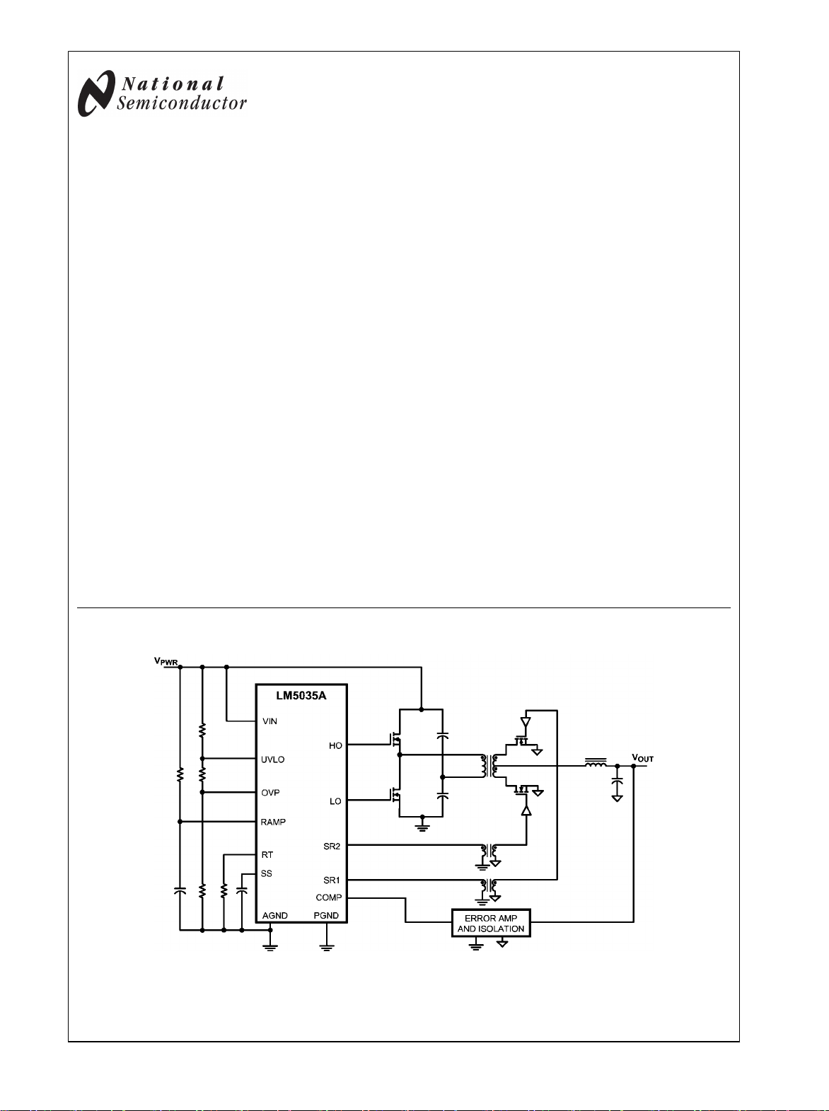
The LM5035A Half-Bridge Controller/Gate Driver contains all
of the features necessary to implement half-bridge topology
power converters using voltage mode control with line voltage
feed-forward. The LM5035A is a functional variant of the
LM5035 half-bridge PWM controller. The VCC current limit
threshold has been increased to 35 mA. The soft start and
soft start currents have been increased from 50 µA to 100 µA.
The BST UV threshold has been lowered to less than the VCC
UV threshold. The ratio of the T1 and T2 delays on the SR1
and SR2 outputs has been increased from 2:1 to 3:1. The
floating high-side gate driver is capable of operating with supply voltages up to 105V. Both the high-side and low-side gate
drivers are capable of 2A peak. An internal high voltage startup regulator is included, along with programmable line undervoltage lockout (UVLO) and overvoltage protection (OVP).
The oscillator is programmed with a single resistor to frequencies up to 2MHz. The oscillator can also be synchronized
to an external clock. A current sense input and a programmable timer provide cycle-by-cycle current limit and adjustable hiccup mode overload protection.
Simplified Application Diagram
Features
105V / 2A Half-Bridge Gate Drivers
■
Synchronous Rectifier Control Outputs with
■
Programmable Delays
High Voltage (105V) Start-up Regulator
■
Voltage mode Control with Line Feed-Forward and Volt •
■
Second Limiting
Resistor Programmed, 2MHz Capable Oscillator
■
Patent Pending Oscillator Synchronization
■
Programmable Line Under-Voltage Lockout
■
Line Over-Voltage Protection
■
Internal Thermal Shutdown Protection
■
Adjustable Soft-Start
■
Versatile Dual Mode Over-Current Protection with Hiccup
■
Delay Timer
Cycle-by-Cycle Over-Current Protection
■
Direct Opto-coupler Interface
■
5V Reference Output
■
Packages
TSSOP-20EP (Thermally enhanced)
■
LLP-24 (4mm x 5mm)
■
30034101
© 2008 National Semiconductor Corporation 300341 www.national.com
Page 2
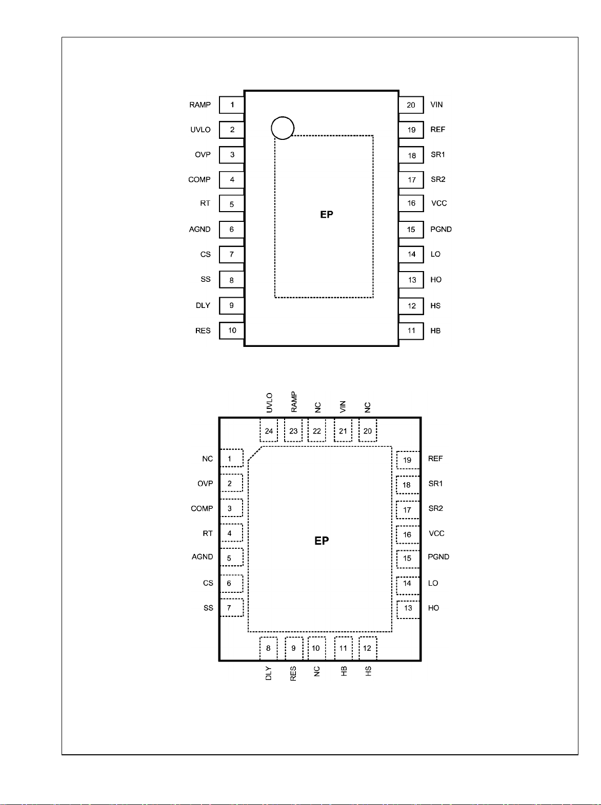
Connection Diagrams
LM5035A
Top View
20-Lead TSSOP EP
30034102
Top View
LLP-24 Package
www.national.com 2
30034103
Page 3

Ordering Information
Order Number Package Type NSC Package Drawing Supplied As
LM5035AMH TSSOP-20EP MXA20A 73 Units per Rail
LM5035AMHX TSSOP-20EP MXA20A 2500 Units on Tape and Reel
LM5035ASQ LLP-24 SQA24B 1000 Units on Tape and Reel
LM5035ASQX LLP-24 SQA24B 4500 Units on Tape and Reel
Pin Descriptions
LM5035A
TSSOP
PIN
LLP PIN Name Description Application Information
1 23 RAMP Modulator ramp signal An external RC circuit from VIN sets the ramp slope. This pin is
discharged at the conclusion of every cycle by an internal FET.
Discharge is initiated by either the internal clock or the Volt •
Second clamp comparator.
2 24 UVLO Line Under-Voltage Lockout An external voltage divider from the power source sets the
shutdown and standby comparator levels. When UVLO reaches
the 0.4V threshold the VCC and REF regulators are enabled.
When UVLO reaches the 1.25V threshold, the SS pin is released
and the device enters the active mode. Hysteresis is set by an
internal current sink that pulls 23 µA from the external resistor
divider.
3 2 OVP Line Over-Voltage Protection An external voltage divider from the power source sets the
shutdown levels. The threshold is 1.25V. Hysteresis is set by an
internal current source that sources 23µA into the external
resistor divider.
4 3 COMP Input to the Pulse Width Modulator An external opto-coupler connected to the COMP pin sources
current into an internal NPN current mirror. The PWM duty cycle
is maximum with zero input current, while 1mA reduces the duty
cycle to zero. The current mirror improves the frequency
response by reducing the AC voltage across the opto-coupler
detector.
5 4 RT Oscillator Frequency Control and
Sync Clock Input.
6 5 AGND Analog Ground Connect directly to Power Ground.
7 6 CS Current Sense input for current
limit
8 7 SS Soft-start Input An internal 110 µA current source charges an external capacitor
9 8 DLY Timing programming pin for the
LO and HO to SR1 and SR2
outputs.
10 9 RES Restart Timer If cycle-by-cycle current limit is exceeded during any cycle, a 22
Normally biased at 2V. An external resistor connected between
RT and AGND sets the internal oscillator frequency. The internal
oscillator can be synchronized to an external clock with a
frequency higher than the free running frequency set by the RT
resistor.
If CS exceeds 0.25V the output pulse will be terminated, entering
cycle-by-cycle current limit. An internal switch holds CS low for
50ns after HO or LO switches high to blank leading edge
transients.
to set the soft-start rate. During a current limit restart sequence,
the internal current source is reduced to 1.2µA to increase the
delay before retry.
An external resistor to ground sets the timing for the non-overlap
time of HO to SR1 and LO to SR2.
µA current is sourced to the RES pin capacitor. If the RES
capacitor voltage reaches 2.5V, the soft-start capacitor will be
fully discharged and then released with a pull-up current of 1.2µA.
After the first output pulse at LO (when SS > COMP offset,
typically 1V), the SS pin charging current will revert to 110 µA.
3 www.national.com
Page 4

TSSOP
PIN
LM5035A
LLP PIN Name Description Application Information
11 11 HB Boost voltage for the HO driver An external diode is required from VCC to HB and an external
capacitor is required from HS to HB to power the HO gate driver.
12 12 HS Switch node Connection common to the transformer and both power switches.
Provides a return path for the HO gate driver.
13 13 HO High side gate drive output. Output of the high side PWM gate driver. Capable of sinking 2A
peak current.
14 14 LO Low side gate drive output. Output of the low side PWM gate driver. Capable of sinking 2A
peak current.
15 15 PGND Power Ground Connect directly to Analog Ground.
16 16 VCC Output of the high voltage start-up
regulator. The VCC voltage is
regulated to 7.6V.
17 17 SR2 Synchronous rectifier driver
output.
18 18 SR1 Synchronous rectifier driver
output.
19 19 REF Output of 5V Reference Maximum output current is 20mA. Locally decoupled with a 0.1µF
20 21 VIN Input voltage source Input to the Start-up Regulator. Operating input range is 13V to
EP EP EP Exposed Pad, underside of
package
1 NC No connection No electrical contact.
10 NC No connection No electrical contact.
20 NC No connection No electrical contact.
22 NC No connection No electrical contact.
If an auxiliary winding raises the voltage on this pin above the
regulation setpoint, the Start-up Regulator will shutdown, thus
reducing the internal power dissipation.
Control output of the synchronous FET gate. Capable of 0.5A
peak current.
Control output of the synchronous FET gate. Capable of 0.5A
peak current.
capacitor.
100V with transient capability to 105V. For power sources outside
of this range, the LM5035A can be biased directly at VCC by an
external regulator.
No electrical contact. Connect to system ground plane for
reduced thermal resistance.
www.national.com 4
Page 5
LM5035A
Absolute Maximum Ratings (Note 1)
If Military/Aerospace specified devices are required,
please contact the National Semiconductor Sales Office/
Distributors for availability and specifications.
VIN to GND -0.3V to 105V
HS to GND -1V to 105V
HB to GND -0.3V to 118V
HB to HS -0.3V to 18V
VCC to GND -0.3V to 16V
All other inputs to GND -0.3V to 7V
ESD Rating (Note 4)
Human Body Model 2kV
Storage Temperature Range -65°C to 150°C
Junction Temperature 150°C
Operating Ratings (Note 1)
VIN Voltage 13V to 105V
External Voltage Applied to VCC 8V to 15V
Operating Junction Temperature -40°C to +125°C
CS, RT, DLY to GND -0.3V to 5.5V
COMP Input Current 10mA
Electrical Characteristics Specifications with standard typeface are for T
apply over full Operating Junction Temperature range. V
27.4kΩ, V
UVLO
= 3V, V
= 0V unless otherwise stated. See (Note 2) and (Note 3).
OVP
= 48V, V
VIN
= 10V externally applied, RRT = 15.0 kΩ, R
VCC
= 25°C, and those with boldface type
J
DLY
Symbol Parameter Conditions Min Typ Max Units
Startup Regulator (VCC pin)
V
VCC
I
VCC(LIM)
V
VCCUV
VCC voltage I
VCC current limit V
VCC Under-voltage threshold (VCC
increasing)
= 10mA 7.3 7.6 7.9 V
VCC
= 7V 25 35 mA
VCC
VIN = VCC, ΔV
from the regulation
VCC
0.2 0.1 V
setpoint
VCC decreasing VCC – PGND 5.5 6.2 6.9 V
I
VIN
Supply current into VCC from
Startup regulator current VIN = 90V, UVLO = 0V 30 70 µA
external source
Outputs & COMP open, V
Outputs Switching
VCC
= 10V,
4 6 mA
Voltage Reference Regulator (REF pin)
V
REF
REF Voltage Regulation I
REF Voltage I
= 0mA 4.85 5 5.15 V
REF
= 0 to 10mA 25 50 mV
REF
REF Current Limit REF = 4.5V 15 20 mA
Under-Voltage Lock Out and shutdown (UVLO pin)
V
I
UVLO
UVLO
Under-voltage threshold 1.212 1.25 1.288 V
Hysteresis current UVLO pin sinking 19 23 27 µA
Under-voltage Shutdown Threshold UVLO voltage falling 0.3 V
Under-voltage Standby Enable
UVLO voltage rising 0.4 V
Threshold
Over-Voltage Protection (OVP pin)
V
I
OVP
OVP
Over-Voltage threshold 1.212 1.25 1.288 V
Hysteresis current OVP pin sourcing 19 23 27 µA
Current Sense Input (CS Pin)
V
CS
CS delay to output CS from zero to 1V. Time for HO and LO
Current Limit Threshold 0.228 0.25 0.272 V
80 ns
to fall to 90% of VCC. Output load = 0 pF.
Leading edge blanking time at CS 50 ns
CS sink impedance (clocked) Internal FET sink impedance 32 60
Current Limit Restart (RES Pin)
V
RES
Charge source current V
Discharge sink current V
RES Threshold 2.4 2.5 2.6 V
= 1.5V 16 22 28 µA
RES
= 1V 8 12 16 µA
RES
=
Ω
5 www.national.com
Page 6
Symbol Parameter Conditions Min Typ Max Units
Soft-Start (SS Pin)
LM5035A
I
SS
Charging current in normal
VSS = 0 80 110 140 µA
operation
Charging current during a hiccup
VSS = 0 0.6 1.2 1.8 µA
mode restart
Soft-stop Current Sink VSS = 2.5V 80 110 140 µA
Oscillator (RT Pin)
F
F
SW1
SW2
Frequency 1 (at HO, half oscillator
frequency)
Frequency 2 (at HO, half oscillator
RRT = 15 kΩ, TJ = 25°C
RRT = 15 kΩ, TJ = -40°C to 125°C
RRT = 5.49 kΩ
185 200 215 kHz
180 220
430 500 570 kHz
frequency)
DC level 2 V
Input Sync threshold 2.5 3 3.4 V
PWM Controller (Comp Pin)
Delay to output 80 ns
V
PWM-OS
SS to RAMP offset 0.7 1 1.2 V
Minimum duty cycle SS = 0V 0 %
Small signal impedance I
= 600µA, COMP current to PWM
COMP
5000
voltage
Main Output Drivers (HO and LO Pins)
Output high voltage I
Output low voltage I
Rise time C
Fall time C
Deadtime, HO to LO, LO to HO V
Peak source current V
Peak sink current V
= 50mA, VHB - VHO, V
OUT
= 100 mA 0.2 0.5 V
OUT
= 1 nF 15 ns
LOAD
= 1 nF 13 ns
LOAD
= V
, I
DLY
HO,LO
HO,LO
REF
= 0V, V
= 10V, V
= 0mA 45 70 100 ns
COMP
= 10V 1.25 A
VCC
= 10V 2 A
VCC
VCC
- V
LO
0.5 0.25 V
HB Threshold VCC rising 3.8 V
Voltage Feed-Forward (RAMP Pin)
RAMP comparator threshold COMP current = 0 2.4 2.5 2.6 V
Synchronous Rectifier Drivers (SR1, SR2)
Output high voltage I
Output low voltage I
Rise time C
Fall time C
Peak source current VSR = 0, V
Peak sink current VSR = V
T1 Deadtime, SR1 falling to HO rising,
SR2 falling to LO rising
T2 Deadtime, HO falling to SR1 rising,
LO falling to SR2 rising
= 10mA, V
OUT
= 20 mA (sink) 0.08 0.2 V
OUT
= 1 nF 40 ns
LOAD
= 1 nF 20 ns
LOAD
VCC
VCC
R
= 10k 33 ns
DLY
R
= 27.4k 68 86 120 ns
DLY
R
= 100k 300 ns
DLY
R
= 10k 18 ns
DLY
R
= 27.4k 20 29 42 ns
DLY
R
= 100k 80 ns
DLY
- V
, V
VCC
SR1
VCC
- V
SR2
0.25 0.1 V
= 10V 0.5 A
, V
= 10V 0.5 A
VCC
Ω
www.national.com 6
Page 7

Symbol Parameter Conditions Min Typ Max Units
Thermal Shutdown
T
SD
Shutdown temperature 165 °C
Hysteresis 20 °C
Thermal Resistance
θ
JA
Junction to ambient, 0 LFPM Air
TSSOP-20_EP package 40 °C/W
Flow
θ
JC
Junction to Case (EP) Thermal
TSSOP-20_EP package 4 °C/W
resistance
θ
JA
θ
JC
Note 1: Absolute Maximum Ratings are limits beyond which damage to the device may occur. Operating Ratings are conditions under which operation of the
device is intended to be functional. For guaranteed specifications and test conditions, see the Electrical Characteristics.
Note 2: All limits are guaranteed. All electrical characteristics having room temperature limits are tested during production with TA = 25°C. All hot and cold limits
are guaranteed by correlating the electrical characteristics to process and temperature variations and applying statistical process control.
Note 3: Typical specifications represent the most likely parametric norm at 25°C operation
Note 4: The human body model is a 100 pF capacitor discharged through a 1.5 kΩ resistor into each pin. 2kV for all pins except HB, HO and HS which are rated
at 1.5kV.
Junction to ambient, 0 LFM Air Flow LLP-24 (4 mm x 5 mm) 40 °C/W
Junction to Case Thermal resistance LLP-24 (4 mm x 5 mm) 6 °C/W
LM5035A
7 www.national.com
Page 8
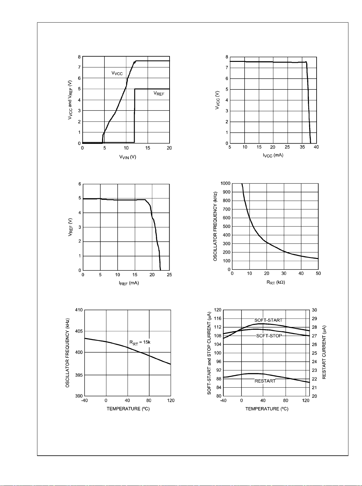
Typical Performance Characteristics
V
LM5035A
VCC
and V
REF
vs V
VIN
V
vs I
VCC
VCC
30034105
V
vs I
REF
REF
30034107
Oscillator Frequency vs Temperature
30034106
Frequency vs RT
30034108
Soft-Start & Stop Current vs Temperature
30034109
www.national.com 8
30034110
Page 9
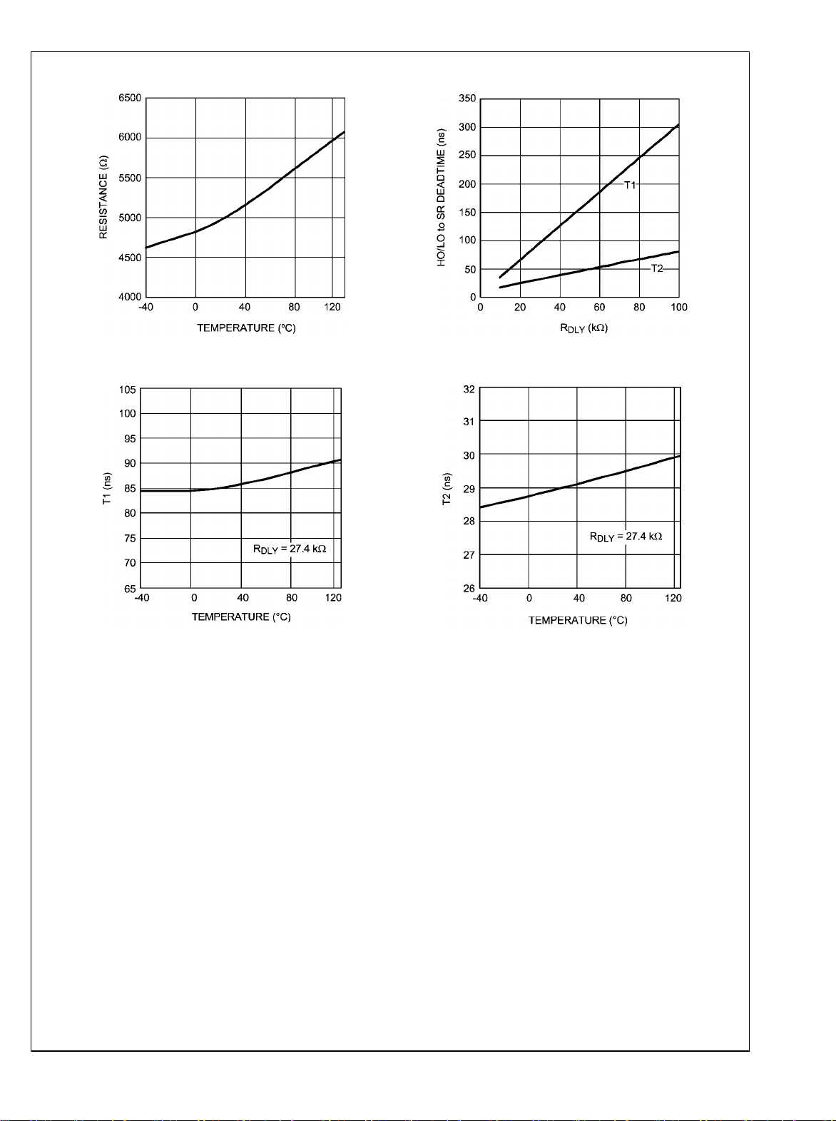
LM5035A
Effective Comp Input Impedance
SR "T1" Parameter vs Temperature
30034111
R
vs Deadtime
DLY
SR "T2" Parameter vs Temperature
30034112
30034113
30034114
9 www.national.com
Page 10

Block Diagram
LM5035A
FIGURE 1.
www.national.com 10
30034104
Page 11

LM5035A
Functional Description
The LM5035A PWM controller contains all of the features
necessary to implement half-bridge voltage-mode controlled
power converters. The LM5035A provides two gate driver
outputs to directly drive the primary side power MOSFETs
and two signal level outputs to control secondary synchronous rectifiers through an isolation interface. Secondary
side drivers, such as the LM5110, are typically used to provide
the necessary gate drive current to control the sync MOSFETs. Synchronous rectification allows higher conversion efficiency and greater power density than conventional PN or
Schottky rectifier techniques. The LM5035A can be configured to operate with bias voltages ranging from 8V to 105V.
Additional features include line under-voltage lockout, cycleby-cycle current limit, voltage feed-forward compensation,
hiccup mode fault protection with adjustable delays, soft-start,
a 2MHz capable oscillator with synchronization capability,
precision reference, thermal shutdown and programmable
volt•second clamping. These features simplify the design of
voltage-mode half-bridge DC-DC power converters. The
Functional Block Diagram is shown in Figure 1.
High-Voltage Start-up Regulator
The LM5035A contains an internal high voltage start-up regulator that allows the input pin (VIN) to be connected directly
to a nominal 48 VDC input voltage. The regulator input can
withstand transients up to 105V. The regulator output at VCC
(7.6V) is internally current limited to 35 mA typical. When the
UVLO pin potential is greater than 0.4V, the VCC regulator is
enabled to charge an external capacitor connected to the
VCC pin. The VCC regulator provides power to the voltage
reference (REF) and the output drivers (LO, SR1 and SR2).
When the voltage on the VCC pin exceeds the UVLO threshold of 7.6V, the internal voltage reference (REF) reaches its
regulation setpoint of 5V and the UVLO voltage is greater than
1.25V, the controller outputs are enabled. The value of the
VCC capacitor depends on the total system design, and its
start-up characteristics. The recommended range of values
for the VCC capacitor is 0.1 µF to 100 µF.
The VCC under-voltage comparator threshold is lowered to
6.2V (typical) after VCC reaches the regulation set-point. If
VCC falls below this value, the outputs are disabled, and the
soft-start capacitor is discharged. If VCC increases above
7.6V, the outputs will be enabled and a soft-start sequence
will commence.
The internal power dissipation of the LM5035A can be reduced by powering VCC from an external supply. In typical
applications, an auxiliary transformer winding is connected
through a diode to the VCC pin. This winding must raise the
VCC voltage above 8.3V to shut off the internal start-up regulator. Powering VCC from an auxiliary winding improves
efficiency while reducing the controller’s power dissipation.
The under-voltage comparator circuit will still function in this
mode, requiring that VCC never falls below 6.2V during the
start-up sequence.
During a fault mode, when the converter auxiliary winding is
inactive, external current draw on the VCC line should be limited such that the power dissipated in the start-up regulator
does not exceed the maximum power dissipation of the IC
package.
An external DC bias voltage can be used instead of the internal regulator by connecting the external bias voltage to both
the VCC and the VIN pins. The external bias must be greater
than 8.3V to exceed the VCC UVLO threshold and less than
the VCC maximum operating voltage rating (15V).
Line Under-Voltage Detector
The LM5035A contains a dual level Under-Voltage Lockout
(UVLO) circuit. When the UVLO pin voltage is below 0.4V, the
controller is in a low current shutdown mode. When the UVLO
pin voltage is greater than 0.4V but less than 1.25V, the controller is in standby mode. In standby mode the VCC and REF
bias regulators are active while the controller outputs are disabled. When the VCC and REF outputs exceed the VCC and
REF under-voltage thresholds and the UVLO pin voltage is
greater than 1.25V, the outputs are enabled and normal operation begins. An external set-point voltage divider from VIN
to GND can be used to set the minimum operating voltage of
the converter. The divider must be designed such that the
voltage at the UVLO pin will be greater than 1.25V when VIN
enters the desired operating range. UVLO hysteresis is accomplished with an internal 23 µA current sink that is switched
on or off into the impedance of the set-point divider. When the
UVLO threshold is exceeded, the current sink is deactivated
to quickly raise the voltage at the UVLO pin. When the UVLO
pin voltage falls below the 1.25V threshold, the current sink is
enabled causing the voltage at the UVLO pin to quickly fall.
The hysteresis of the 0.4V shutdown comparator is internally
fixed at 100 mV.
The UVLO pin can also be used to implement various remote
enable / disable functions. Turning off a converter by forcing
the UVLO pin to the standby condition provides a controlled
soft-stop. See the Soft Start section for more details.
Line Over Voltage / Load Over Voltage / Remote Thermal Protection
The LM5035A provides a multipurpose OVP pin that supports
several fault protection functions. When the OVP pin voltage
exceeds 1.25V, the controller is held in standby mode which
immediately halts the PWM pulses at the HO and LO pins. In
standby mode, the VCC and REF bias regulators are active
while the controller outputs are disabled. When the OVP pin
voltage falls below the 1.25V OVP threshold, the outputs are
enabled and normal soft-start sequence begins. Hysteresis is
accomplished with an internal 23 µA current source that is
switched on or off into the impedance of the OVP pin set-point
divider. When the OVP threshold is exceeded, the current
source is enabled to quickly raise the voltage at the OVP pin.
When the OVP pin voltage falls below the 1.25V threshold,
the current source is disabled causing the voltage at the OVP
pin to quickly fall.
Several examples of the use of this pin are provided in the
Application Information section.
Reference
The REF pin is the output of a 5V linear regulator that can be
used to bias an opto-coupler transistor and external housekeeping circuits. The regulator output is internally current
limited to 20mA (typical).
11 www.national.com
Page 12

Cycle-by-Cycle Current Limit
The CS pin is driven by a signal representative of the transformer primary current. If the voltage sensed at CS pin ex-
LM5035A
ceeds 0.25V, the current sense comparator terminates the
HO or LO output driver pulse. If the high current condition
persists, the controller operates in a cycle-by-cycle current
limit mode with duty cycle determined by the current sense
comparator instead of the PWM comparator. Cycle-by-cycle
current limiting may trigger the hiccup mode restart cycle depending on the configuration of the RES pin (see below).
A small R-C filter connect to the CS pin and located near the
controller is recommended to suppress noise. An internal
32Ω MOSFET connected to the CS input discharges the external current sense filter capacitor at the conclusion of every
cycle. The discharge MOSFET remains on for an additional
50 ns after the HO or LO driver switches high to blank leading
edge transients in the current sensing circuit. Discharging the
CS pin filter each cycle and blanking leading edge spikes reduces the filtering requirements and improves the current
sense response time.
The current sense comparator is very fast and responds to
short duration noise pulses. Layout considerations are critical
for the current sense filter and sense resistor. The capacitor
associated with the CS filter must be placed very close to the
device and connected directly to the CS and AGND pins. If a
current sense transformer is used, both leads of the transformer secondary should be routed to the filter network, which
should be located close to the IC. If a sense resistor located
in the source of the main MOSFET switch is used for current
sensing, a low inductance type of resistor is required. When
designing with a current sense resistor, all of the noise sensitive low power ground connections should be connected
together near the AGND pin, and a single connection should
be made to the power ground (sense resistor ground point).
Overload Protection Timer
The LM5035A provides a current limit restart timer to disable
the outputs and force a delayed restart (hiccup mode) if a
current limit condition is repeatedly sensed. The number of
cycle-by-cycle current limit events required to trigger the
restart is programmable by the external capacitor at the RES
pin. During each PWM cycle, the LM5035A either sources or
sinks current from the RES pin capacitor. If no current limit is
detected during a cycle, an 12 µA discharge current sink is
enabled to pull the RES pin to ground. If a current limit is detected, the 12 µA sink current is disabled and a 22µA current
source causes the voltage at the RES pin to gradually increase. The LM5035A protects the converter with cycle-bycycle current limiting while the voltage at RES pin increases.
If the RES voltage reaches the 2.5V threshold, the following
restart sequence occurs (also see Figure 2):
•
The RES capacitor and SS capacitors are fully discharged
•
The soft-start current source is reduced from 110 µA to 1
µA
•
The SS capacitor voltage slowly increases. When the SS
voltage reaches ≊1V, the PWM comparator will produce
the first narrow output pulse. After the first pulse occurs,
the SS source current reverts to the normal 110 µA level.
The SS voltage increases at its normal rate, gradually
increasing the duty cycle of the output drivers
•
If the overload condition persists after restart, cycle-bycycle current limiting will begin to increase the voltage on
the RES capacitor again, repeating the hiccup mode
sequence
•
If the overload condition no longer exists after restart, the
RES pin will be held at ground by the 12 µA current sink
and normal operation resumes
The overload timer function is very versatile and can be configured for the following modes of protection:
1. Cycle-by-cycle only: The hiccup mode can be completely
disabled by connecting a zero to 50 kΩ resistor from the RES
pin to AGND. In this configuration, the cycle-by-cycle protection will limit the output current indefinitely and no hiccup
sequences will occur.
2. Hiccup only: The timer can be configured for immediate
activation of a hiccup sequence upon detection of an overload
by leaving the RES pin open circuit.
3. Delayed Hiccup: Connecting a capacitor to the RES pin
provides a programmed interval of cycle-by-cycle limiting before initiating a hiccup mode restart, as previously described.
The dual advantages of this configuration are that a short term
overload will not cause a hiccup mode restart but during extended overload conditions, the average dissipation of the
power converter will be very low.
4. Externally Controlled Hiccup: The RES pin can also be
used as an input. By externally driving the pin to a level
greater than the 2.5V hiccup threshold, the controller will be
forced into the delayed restart sequence. For example, the
external trigger for a delayed restart sequence could come
from an over-temperature protection circuit or an output overvoltage sensor.
www.national.com 12
Page 13

30034115
LM5035A
FIGURE 2. Current Limit Restart Circuit
FIGURE 3. Current Limit Restart Timing
30034116
13 www.national.com
Page 14

LM5035A
30034117
FIGURE 4. Optocoupler to COMP Interface
Soft-Start
The soft-start circuit allows the regulator to gradually reach a
steady state operating point, thereby reducing start-up stresses and current surges. When bias is supplied to the LM5035A,
the SS pin capacitor is discharged by an internal MOSFET.
When the UVLO, VCC and REF pins reach their operating
thresholds, the SS capacitor is released and charged with a
110 µA current source. The PWM comparator control voltage
is clamped to the SS pin voltage by an internal amplifier.
When the PWM comparator input reaches 1V, output pulses
commence with slowly increasing duty cycle. The voltage at
the SS pin eventually increases to 5V, while the voltage at the
PWM comparator increases to the value required for regulation as determined by the voltage feedback loop.
One method to shutdown the regulator is to ground the SS
pin. This forces the internal PWM control signal to ground,
reducing the output duty cycle quickly to zero. Releasing the
SS pin begins a soft-start cycle and normal operation resumes. A second shutdown method is discussed in the UVLO
section.
Soft-Stop
If the UVLO pin voltage falls below the 1.25V standby threshold but above the 0.4V shutdown threshold, the 110 µA SS
pin source current is disabled and a 110 µA sink current discharges the soft-start capacitor. As SS voltage falls and
clamps the PWM comparator input, the PWM duty cycle will
gradually fall to zero. The soft-stop feature produces a gradual reduction of the power converter output voltage. This softstop method of turning off the converter reduces energy in the
output capacitor before control of the main and synchronous
rectification MOSFETs is disabled. The PWM pulses may
cease before the SS voltage reduces the duty cycle if the VCC
or REF voltage drops below the respective under-voltage
thresholds during the soft-stop process.
PWM Comparator
The pulse width modulation (PWM) comparator compares the
voltage ramp signal at the RAMP pin to the loop error signal.
This comparator is optimized for speed in order to achieve
minimum controllable duty cycles. The loop error signal is received from the external feedback and isolation circuit is in
the form of a control current into the COMP pin. The COMP
pin current is internally mirrored by a matched pair of NPN
transistors which sink current through a 5 kΩ resistor connected to the 5V reference. The resulting control voltage
passes through a 1V level shift before being applied to the
PWM comparator.
An opto-coupler detector can be connected between the REF
pin and the COMP pin. Because the COMP pin is controlled
by a current input, the potential difference across the optocoupler detector is nearly constant. The bandwidth limiting
phase delay which is normally introduced by the significant
capacitance of the opto-coupler is thereby greatly reduced.
Higher loop bandwidths can be realized since the bandwidthlimiting pole associated with the opto-coupler is now at a
much higher frequency. The PWM comparator polarity is configured such that with no current into the COMP pin, the
controller produces the maximum duty cycle at the main gate
driver outputs, HO and LO.
Feed-Forward Ramp and Volt • Second Clamp
An external resistor (RFF) and capacitor (CFF) connected to
VIN, AGND, and the RAMP pin are required to create the
PWM ramp signal. The slope of the signal at RAMP will vary
in proportion to the input line voltage. This varying slope provides line feed-forward information necessary to improve line
transient response with voltage mode control. The RAMP signal is compared to the error signal by the pulse width modulator comparator to control the duty cycle of the HO and LO
outputs. With a constant error signal, the on-time (TON) varies
inversely with the input voltage (VIN) to stabilize the Volt •
Second product of the transformer primary signal. The power
path gain of conventional voltage-mode pulse width modulators (oscillator generated ramp) varies directly with input voltage. The use of a line generated ramp (input voltage feedforward) nearly eliminates this gain variation. As a result, the
feedback loop is only required to make very small corrections
for large changes in input voltage.
In addition to the PWM comparator, a Volt • Second Clamp
comparator also monitors the RAMP pin. If the ramp amplitude exceeds the 2.5V threshold of the Volt • Second Clamp
comparator, the on-time is terminated. The CFF ramp capacitor is discharged by an internal 32Ω discharge MOSFET
controlled by the V•S Clamp comparator. If the RAMP signal
does not exceed 2.5V before the end of the clock period, then
the internal clock will enable the discharge MOSFET to reset
capacitor CFF.
By proper selection of RFF and CFF values, the maximum ontime of HO and LO can be set to the desired duration. The ontime set by the Volt • Second Clamp varies inversely to the
line voltage because the RAMP capacitor is charged by a re-
www.national.com 14
Page 15

LM5035A
sistor (RFF) connected to VIN while the threshold of the clamp
is a fixed voltage (2.5V). An example will illustrate the use of
the Volt • Second Clamp comparator to achieve a 50% duty
cycle limit at 200kHz with a 48V line input. A 50% duty cycle
at a 200kHz requires a 2.5µs on-time. To achieve this maximum on-time clamp level:
The recommended capacitor value range for CFF is 100 pF to
1000 pF. 470 pF is a standard value that can be paired with
an 110 kΩ to approximate the desired 51.4µs time constant.
If load transient response is slowed by the 10% margin, the
RFF value can be increased. The system signal-to-noise will
be slightly decreased by increasing RFF x CFF.
Oscillator, Sync Capability
The LM5035A oscillator frequency is set by a single external
resistor connected between the RT and AGND pins. To set a
desired oscillator frequency, the necessary RT resistor is calculated from:
For example, if the desired oscillator frequency is 400kHz (HO
and LO each switching at 200 kHz) a 15 kΩ resistor would be
the nearest standard one percent value.
Each output (HO, LO, SR1 and SR2) switches at half the oscillator frequency. The voltage at the RT pin is internally
regulated to a nominal 2V. The RT resistor should be located
as close as possible to the IC, and connected directly to the
pins (RT and AGND). The tolerance of the external resistor,
and the frequency tolerance indicated in the Electrical Characteristics, must be taken into account when determining the
worst case frequency range.
The LM5035A can be synchronized to an external clock by
applying a narrow pulse to the RT pin. The external clock must
be at least 10% higher than the free-running oscillator frequency set by the RT resistor. If the external clock frequency
is less than the RT resistor programmed frequency, the
LM5035A will ignore the synchronizing pulses. The synchronization pulse width at the RT pin must be a minimum of 15
ns wide. The clock signal should be coupled into the RT pin
through a 100 pF capacitor or a value small enough to ensure
the pulse width at RT is less than 60% of the clock period
under all conditions. When the synchronizing pulse transitions low-to-high (rising edge), the voltage at the RT pin must
be driven to exceed 3.2V volts from its nominal 2 VDC level.
During the clock signal’s low time, the voltage at the RT pin
will be clamped at 2 VDC by an internal regulator. The output
impedance of the RT regulator is approximately 100Ω. The
RT resistor is always required, whether the oscillator is free
running or externally synchronized.
Gate Driver Outputs (HO & LO)
The LM5035A provides two alternating gate driver outputs,
the floating high side gate driver HO and the ground referenced low side driver LO. Each driver is capable of sourcing
1.25A and sinking 2A peak. The HO and LO outputs operate
in an alternating manner, at one-half the internal oscillator
frequency. The LO driver is powered directly by the VCC regulator. The HO gate driver is powered from a bootstrap capacitor connected between HB and HS. An external diode
connected between VCC (anode pin) and HB (cathode pin)
provides the high side gate driver power by charging the bootstrap capacitor from VCC when the switch node (HS pin) is
low. When the high side MOSFET is turned on, HB rises to a
peak voltage equal to V
node voltage.
The HB and VCC capacitors should be placed close to the
pins of the LM5035A to minimize voltage transients due to
parasitic inductances since the peak current sourced to the
MOSFET gates can exceed 1.25A. The recommended value
of the HB capacitor is 0.01 µF or greater. A low ESR / ESL
capacitor, such as a surface mount ceramic, should be used
to prevent voltage droop during the HO transitions.
The maximum duty cycle for each output is limited to slightly
less than 50% due to the internally fixed deadtime. If the
COMP pin is open circuit, the outputs will operate at maximum
duty cycle. The typical deadtime in this condition is 70ns
which does not vary with operating frequency. The maximum
duty cycle for each output can be calculated with the following
equation:
where TS is the period of one complete cycle for both HO and
LO outputs, and TD is the deadtime. For example, if the oscillator frequency is 200 kHz, each output will cycle at 100 kHz
(TS = 10 µs). Using the nominal deadtime of 70ns, the maximum duty cycle at this frequency is calculated to be 49.3%.
+ VHS where VHS is the switch
VCC
15 www.national.com
Page 16

LM5035A
30034121
FIGURE 5. HO, LO, SR1 and SR2 Timing Diagram
Synchronous Rectifier Control Outputs (SR1 & SR2)
Synchronous rectification (SR) of the transformer secondary
provides higher efficiency, especially for low output voltage
converters. The reduction of rectifier forward voltage drop
(0.5V - 1.5V) to 10mV - 200mV VDS voltage for a MOSFET
significantly reduces rectification losses. In a typical application, the transformer secondary winding is center tapped, with
the output power inductor in series with the center tap. The
SR MOSFETs provide the ground path for the energized secondary winding and the inductor current. Figure 5 shows that
the SR2 MOSFET is conducting while HO enables power
transfer from the primary. The SR1 MOSFET must be disabled during this period since the secondary winding connected to the SR1 MOSFET drain is twice the voltage of the
center tap. At the conclusion of the HO pulse, the inductor
current continues to flow through the SR1 MOSFET body
diode. Since the body diode causes more loss than the SR
MOSFET, efficiency can be improved by minimizing the T2
period while maintaining sufficient timing margin over all conditions (component tolerances, etc.) to prevent shoot-through
current. When LO enables power transfer from the primary,
the SR1 MOSFET is enabled and the SR2 MOSFET is off.
During the time that neither HO nor LO is active, the inductor
current is shared between both the SR1 and SR2 MOSFETs
which effectively shorts the transformer secondary and cancels the inductance in the windings. The SR2 MOSFET is
disabled before LO delivers power to the secondary to prevent power being shunted to ground. The SR2 MOSFET body
diode continues to carry about half the inductor current until
the primary power raises the SR2 MOSFET drain voltage and
reverse biases the body diode. Ideally, dead-time T1 would
be set to the minimum time that allows the SR MOSFET to
turn off before the SR MOSFET body diode starts conducting.
The SR1 and SR2 outputs are powered directly by the VCC
regulator. Each output is capable of sourcing and sinking 0.5A
peak. Typically, the SR1 and SR2 signals control SR MOSFET gate drivers through a pulse transformer. The actual gate
sourcing and sinking currents are provided by the secondaryside bias supply and gate drivers.
The timing of SR1 and SR2 with respect to HO and LO is
shown in Figure 5. SR1 is configured out of phase with HO
and SR2 is configured out of phase with LO. The deadtime
between transitions is programmable by a resistor connected
from the DLY pin to the AGND pin. Typically, R
the range of 10kΩ to 100kΩ. The deadtime periods can be
calculated using the following formulae:
T1 = .003 x R
T2 = .0007 x R
To set the minimum (propagation delays only) deadtime, the
DLY pin should be left open or connected to the REF pin. Any
resistor value above 300kΩ connected between the DLY pin
and AGND will also provide the minimum period (approximately 5 ns).
+ 4.6 ns
DLY
+ 10.01 ns
DLY
is set in
DLY
Thermal Protection
Internal Thermal Shutdown circuitry is provided to protect the
integrated circuit in the event the maximum rated junction
temperature is exceeded. When activated, typically at 165°C,
the controller is forced into a low power standby state with the
output drivers (HO, LO, SR1 and SR2), the bias regulators
(VCC and REF) disabled. This helps to prevent catastrophic
failures from accidental device overheating. During thermal
shutdown, the soft-start capacitor is fully discharged and the
controller follows a normal start-up sequence after the junction temperature falls to the operating level (145°C).
www.national.com 16
Page 17

LM5035A
Applications Information
The following information is intended to provide guidelines for
the power supply designer using the LM5035A.
VIN
The voltage applied to the VIN pin, which may be the same
as the system voltage applied to the power transformer’s primary (V
into VIN depends primarily on the gate charge provided to the
output drivers, the switching frequency, and any external
loads on the VCC and REF pins. It is recommended the filter
shown in Figure 6 be used to suppress transients which may
occur at the input supply. This is particularly important when
VIN is operated close to the maximum operating rating of the
LM5035A.
When power is applied to VIN and the UVLO pin voltage is
greater than 0.4V, the VCC regulator is enabled and supplies
current into an external capacitor connected to the VCC pin.
When the voltage on the VCC pin reaches the regulation point
of 7.6V, the voltage reference (REF) is enabled. The reference regulation set point is 5V. The HO, LO, SR1 and SR2
outputs are enabled when the two bias regulators reach their
set point and the UVLO pin potential is greater than 1.25V. In
typical applications, an auxiliary transformer winding is connected through a diode to the VCC pin. This winding must
raise the VCC voltage above 8.3V to shut off the internal startup regulator.
After the outputs are enabled and the external VCC supply
voltage has begun supplying power to the IC, the current into
VIN drops below 1 mA. VIN should remain at a voltage equal
to or above the VCC voltage to avoid reverse current through
protection diodes.
), can vary in the range of 13 to 105V. The current
PWR
FOR APPLICATIONS >100V
For applications where the system input voltage exceeds
100V or the IC power dissipation is of concern, the LM5035A
can be powered from an external start-up regulator as shown
in Figure 7. In this configuration, the VIN and the VCC pins
should be connected together, which allows the LM5035A to
be operated below 13V. The voltage at the VCC pin must be
greater than 8.3V yet not exceed 15V. An auxiliary winding
can be used to reduce the power dissipation in the external
regulator once the power converter is active. The NPN baseemitter reverse breakdown voltage, which can be as low as
5V for some transistors, should be considered when selecting
the transistor.
CURRENT SENSE
The CS pin needs to receive an input signal representative of
the transformer’s primary current, either from a current sense
transformer or from a resistor in series with the source of the
LO switch, as shown in Figure 8 and Figure 9. In both cases,
the sensed current creates a ramping voltage across R1, and
the RF/CF filter suppresses noise and transients. R1, RF and
CF should be located as close to the LM5035A as possible,
and the ground connection from the current sense transformer, or R1, should be a dedicated track to the AGND pin.
The current sense components must provide greater than
0.25V at the CS pin when an over-current condition exists.
30034122
FIGURE 6. Input Transient Protection
FIGURE 7. Start-up Regulator for V
30034124
PWR
30034123
>100V
FIGURE 8. Current Sense Using Current Sense Transformer
17 www.national.com
Page 18

LM5035A
30034125
FIGURE 9. Current Sense Using Current Sense Resistor (R1)
If the current sense resistor method is used, the over-current
condition will only be sensed while LO is driving the low-side
MOSFET. Over-current while HO is driving the high-side
MOSFET will not be detected. In this configuration, it will take
4 times as long for continuous cycle-by-cycle current limiting
to initiate a restart event since each over-current event during
LO enables the 22µA RES pin current source for one oscillator
period, and then the lack of an over-current event during HO
enables the 12µA RES pin current sink for one oscillator period. The time average of this toggling is equivalent to a
continuous 5 µA current source into the RES capacitor, increasing the delay by a factor of four. The value of the RES
capacitor can be reduced to decrease the time before restart
cycle is initiated.
When using the resistor current sense method, an imbalance
in the input capacitor voltages may develop when operating
in cycle-by-cycle current limiting mode. If the imbalance persists for an extended period, excessive currents in the nonsensed MOSFET, and possible transformer saturation may
result. This condition is inherent to the half-bridge topology
operated with cycle-by-cycle current limiting and is compounded by only sensing in one leg of the half-bridge circuit.
The imbalance is greatest at large duty cycles (low input voltages). If using this method, it is recommended that the capacitor on the RES pin be no larger than 220 pF. Check the
final circuit and reduce the RES capacitor further, or omit the
capacitor completely to ensure the voltages across the bridge
capacitors remain balanced. The current limit value may decrease slightly as the RES capacitor is reduced.
HO, HB, HS and LO
Attention must be given to the PC board layout for the lowside driver and the floating high-side driver pins HO, HB and
HS. A low ESR/ESL capacitor (such as a ceramic surface
mount capacitor) should be connected close to the LM5035A,
between HB and HS to provide high peak currents during turnon of the high-side MOSFET. The capacitor should be large
enough to supply the MOSFET gate charge (Qg) without discharging to the point where the drop in gate voltage affects
the MOSFET R
ommended.
. A value ten to twenty times Qg is rec-
DS(ON)
The diode (D
low-side MOSFET is conducting should be capable of with-
) that charges C
BOOST
from VCC when the
BOOST
standing the full converter input voltage range. When the
high-side MOSFET is conducting, the reverse voltage at the
diode is approximately the same as the MOSFET drain voltage because the high-side driver is boosted up to the converter input voltage by the HS pin, and the high side MOSFET
gate is driven to the HS voltage plus VCC. Since the anode
of D
the diode is equal to the input voltage minus the VCC voltage.
D
BOOST
tions, so a low current ultra-fast recovery diode is recom-
is connected to VCC, the reverse potential across
BOOST
average current is less than 20mA in most applica-
mended to limit the loss due to diode junction capacitance.
Schottky diodes are also a viable option, particularly for lower
input voltage applications, but attention must be paid to leakage currents at high temperatures.
The internal gate drivers need a very low impedance path to
the respective decoupling capacitors; the VCC cap for the LO
driver and C
should be as short as possible to reduce inductance and as
for the HO driver. These connections
BOOST
wide as possible to reduce resistance. The loop area, defined
by the gate connection and its respective return path, should
be minimized.
The high-side gate driver can also be used with HS connected
to PGND for applications other than a half bridge converter
(e.g. Push-Pull). The HB pin is then connected to VCC, or any
supply greater than the high-side driver undervoltage lockout
(approximately 6.5V). In addition, the high-side driver can be
configured for high voltage offline applications where the
high-side MOSFET gate is driven via a gate drive transformer.
PROGRAMMABLE DELAY (DLY)
The R
SR2 signals and the HO and LO driver outputs. Figure 5
resistor programs the delays between the SR1 and
DLY
shows the relationship between these outputs. The DLY pin
is nominally set at 2.5V and the current is sensed through
R
to ground. This current is used to adjust the amount of
DLY
deadtime before the HO and LO pulse (T1) and after the HO
and LO pulse (T2). Typically R
100kΩ. The deadtime periods can be calculated using the
is in the range of 10kΩ to
DLY
following formulae:
T1 = .003 x R
+ 4.6 ns
DLY
www.national.com 18
Page 19

LM5035A
T2 = .0007 x R
+ 10.01 ns
DLY
T1 and T2 can be set to minimum by not connecting a resistor
to DLY, connecting a resistor greater than 300kΩ from DLY
to ground, or connecting DLY to the REF pin. This may cause
lower than optimal system efficiency if the delays through the
SR signal transformer network, the secondary gate drivers
and the SR MOSFETs are greater than the delay to turn on
the HO or LO MOSFETs. Should an SR MOSFET remain on
while the opposing primary MOSFET is supplying power
through the power transformer, the secondary winding will
experience a momentary short circuit, causing a significant
power loss to occur.
When choosing the R
lays and component tolerances should be considered to as-
value, worst case propagation de-
DLY
sure that there is never a time where both SR MOSFETs are
enabled AND one of the primary side MOSFETs is enabled.
The time period T1 should be set so that the SR MOSFET has
turned off before the primary MOSFET is enabled. Conversely, T1 and T2 should be kept as low as tolerances allow to
optimize efficiency. The SR body diode conducts during the
time between the SR MOSFET turns off and the power transformer begins supplying energy. Power losses increase when
this happens since the body diode voltage drop is many times
higher than the MOSFET channel voltage drop. The interval
of body diode conduction can be observed with an oscilloscope as a negative 0.7V to 1.5V pulse at the SR MOSFET
drain.
UVLO AND OVP VOLTAGE DIVIDER SELECTION FOR R1, R2, AND R3
Two dedicated comparators connected to the UVLO and OVP
pins are used to detect under-voltage and over-voltage conditions. The threshold value of these comparators, V
V
, is 1.25V (typical). The two functions can be pro-
OVP
grammed independently with two voltage dividers from VIN to
UVLO
and
AGND as shown in Figure 10 and Figure 11, or with a threeresistor divider as shown in Figure 12. Independent UVLO
and OVP pins provide greater flexibility for the user to select
the operational voltage range of the system. Hysteresis is accomplished by 23 µA current sources (I
are switched on or off into the sense pin resistor dividers as
UVLO
and I
OVP
), which
the comparators change state.
When the UVLO pin voltage is below 0.4V, the controller is in
a low current shutdown mode. For a UVLO pin voltage greater
than 0.4V but less than 1.25V the controller is in standby
mode. Once the UVLO pin voltage is greater than 1.25V, the
controller is fully enabled. Two external resistors can be used
to program the minimum operational voltage for the power
converter as shown in Figure 10. When the UVLO pin voltage
falls below the 1.25V threshold, an internal 23 µA current sink
is enabled to lower the voltage at the UVLO pin, thus providing
threshold hysteresis. Resistance values for R1 and R2 can
be determined from the following equations.
where V
desired UVLO hysteresis at V
For example, if the LM5035A is to be enabled when V
reaches 34V, and disabled when VPWR is decreased to 32V,
is the desired turn-on voltage and V
PWR
PWR
.
HYS
is the
PWR
R1 should be 87 kΩ, and R2 should be 3.54kΩ. The voltage
at the UVLO pin should not exceed 7V at any time. Be sure
to check both the power and voltage rating (0603 resistors
can be rated as low as 50V) for the selected R1 resistor.
FIGURE 10. Basic UVLO Configuration
19 www.national.com
30034129
Page 20

LM5035A
30034130
FIGURE 11. Basic Over-Voltage Protection
FIGURE 12. UVLO/OVP Divider
The impedance seen looking into the resistor divider from the
UVLO and OVP pins determines the hysteresis level. UVLO
the equations in the table below for the three-resistor divider
illustrated in Figure 12.
and OVP enable and disable thresholds are calculated using
TABLE 1. UVO/OVP Divider Formulas
Outputs disabled due to VIN falling below UVLO threshold
Outputs enabled due to VIN rising above UVLO threshold UVLOon = UVLO
Outputs disabled due to VIN rising above OVP threshold
Outputs enabled due to VIN falling below OVP threshold OVP
The typical operating ranges of undervoltage and overvoltage
thresholds are calculated from the above equations. For example, for resistor values R1 = 86.6kΩ, R2 = 2.10kΩ and R3
= 1.40kΩ the computed thresholds are:
= OVP
on
UVLO turn-off = 32.2V
UVLO turn-on = 34.2V
OVP turn-on = 78.4V
OVP turn-off = 80.5V
30034131
+ (23 µA x R1)
off
- [23 µA x (R1 + R2)]
off
www.national.com 20
Page 21

FIGURE 13. Remote Standby and Disable Control
LM5035A
30034136
To maintain the threshold’s accuracy, a resistor tolerance of
1% or better is recommended.
The design process starts with the choice of the voltage difference between the UVLO enabling and disabling thresholds. This will also approximately set the difference between
OVP enabling and disabling regulation:
Next, the combined resistance of R2 and R3 is calculated by
choosing the threshold for the UVLO disabling threshold:
Then R3 is determined by selecting the OVP disabling threshold:
Finally, R3 is subtracted from R
COMBINED
to give R2:
R2 = R
COMBINED
- R
3
Remote configuration of the controller’s operational modes
can be accomplished with open drain device(s) connected to
the UVLO pin as shown in Figure 13.
FAULT PROTECTION
The Over Voltage Protection (OVP) comparator of the
LM5035A can be configured for line or load fault protection or
thermal protection using an external temperature sensor or
thermistor. Figure 11 shows a line over voltage shutdown application using a voltage divider between the input power
supply, V
, and AGND to monitor the line voltage.
PWR
Figure 14 demonstrates the use of the OVP pin for latched
output over-voltage fault protection, using a zener and optocoupler. When V
opto-coupler diode and zener, the opto-coupler momentarily
exceeds the conduction threshold of the
OUT
turns on Q1 and the LM5035A enters standby mode, disabling
the drivers and enabling the hysteresis current source on the
OVP pin. Once the current source is enabled, the OVP voltage will remain at 2.3V (23 µA x 100 kΩ) without additional
drive from the external circuit. If the opto-coupler transistor
emitter were directly connected to the OVP pin, then leakage
current in the zener diode amplified by the opto-coupler’s gain
could falsely trip the protection latch. R1 and Q1 are added
reduce the sensitivity to low level currents in the opto-coupler.
Using the values of Figure 14, the opto-coupler collector current must equal V
Once the controller has switched to standby mode, the out-
/ R1 = 350 µA before OVP latches.
BE(Q1)
puts no longer switch but the VCC and REF regulators continue functioning and supply bias to the external circuitry. VCC
must fall below 6.2V or the UVLO pin must fall below 0.4V to
clear the OVP latch.
21 www.national.com
Page 22

LM5035A
30034137
FIGURE 14. Latched Load Over-Voltage Protection
Figure 15 shows an application of the OVP comparator for
Remote Thermal Protection using a thermistor (or multiple
thermistors) which may be located near the main heat
sources of the power supply. The negative temperature coefficient (NTC) thermistor is nearly logarithmic, and in this
example a 100kΩ thermistor with the β material constant of
4500 kelvins changes to approximately 2 kΩ at 130°C. Setting
R1 to one-third of this resistance (665Ω) establishes 130°C
as the desired trip point (for V
= 5V). In a temperature band
REF
FIGURE 15. Remote Thermal Protection
HICCUP MODE CURRENT LIMIT RESTART (RES)
The basic operation of the hiccup mode current limit restart is
described in the functional description. The delay time to
restart is programmed with the selection of the RES pin capacitor C
as illustrated in Figure 15.
RES
In the case of continuous cycle-by-cycle current limit detection at the CS pin, the time required for C
hiccup mode threshold is:
For example, if C
1.14 ms.
= 0.01 µF the time t1 is approximately
RES
to reach the 2.5V
RES
The cool down time, t2 is set by the soft-start capacitor (CSS)
and the internal 1 µA SS current source, and is equal to:
from 20°C below to 20°C above the OVP threshold, the voltage divider is nearly linear with 25 mV per°C sensitivity.
R2 provides temperature hysteresis by raising the OVP comparator input by R2 x 23 µA. For example, if a 22kΩ resistor
is selected for R2, then the OVP pin voltage will increase by
22 kΩ x 23 µA = 506 mV. The NTC temperature must therefore fall by 506mV / 25mV per°C = 20°C before the LM5035A
switches from the standby mode to the normal mode.
30034138
If CSS = 0.01 µF t2 is ≊10 ms.
The soft-start time t3 is set by the internal 110 µA current
source, and is equal to:
If CSS = 0.01 µF t3 is ≊363 µs.
The time t2 provides a periodic cool-down time for the power
converter in the event of a sustained overload or short circuit.
This off time results in lower average input current and lower
power dissipation within the power components. It is recommended that the ratio of t2 / (t1 + t3) be in the range of 5 to
10 to take advantage of this feature.
If the application requires no delay from the first detection of
a current limit condition to the onset of the hiccup mode (t1 =
0), the RES pin can be left open (no external capacitor). If it
is desired to disable the hiccup mode entirely, the RES pin
should be connected to ground (AGND).
www.national.com 22
Page 23

FIGURE 16. Hiccup Over-Load Restart Timing
LM5035A
30034116
23 www.national.com
Page 24

Printed Circuit Board Layout
The LM5035A Current Sense and PWM comparators are very
fast, and respond to short duration noise pulses. The compo-
LM5035A
nents at the CS, COMP, SS, OVP, UVLO, DLY and the RT
pins should be as physically close as possible to the IC, thereby minimizing noise pickup on the PC board tracks.
Layout considerations are critical for the current sense filter.
If a current sense transformer is used, both leads of the transformer secondary should be routed to the sense filter components and to the IC pins. The ground side of the transformer
should be connected via a dedicated PC board track to the
AGND pin, rather than through the ground plane.
If the current sense circuit employs a sense resistor in the
drive transistor source, low inductance resistors should be
used. In this case, all the noise sensitive, low-current ground
tracks should be connected in common near the IC, and then
a single connection made to the power ground (sense resistor
ground point).
The gate drive outputs of the LM5035A should have short,
direct paths to the power MOSFETs in order to minimize inductance in the PC board traces. The SR control outputs
should also have minimum routing distance through the pulse
transformers and through the secondary gate drivers to the
sync FETs.
The two ground pins (AGND, PGND) must be connected together with a short, direct connection, to avoid jitter due to
relative ground bounce.
If the internal dissipation of the LM5035A produces high junction temperatures during normal operation, the use of multiple
vias under the IC to a ground plane can help conduct heat
away from the IC. Judicious positioning of the PC board within
the end product, along with use of any available air flow
(forced or natural convection) will help reduce the junction
temperatures. If using forced air cooling, avoid placing the
LM5035A in the airflow shadow of tall components, such as
input capacitors.
Application Circuit Example
The following schematic shows an example of a 100W halfbridge power converter controlled by the LM5035A. The operating input voltage range (V
output voltage is 3.3V. The output current capability is 30
Amps. Current sense transformer T2 provides information to
the CS pin for current limit protection. The error amplifier and
reference, U3 and U5 respectively, provide voltage feedback
via opto-coupler U4. Synchronous rectifiers Q4, Q5, Q6 and
Q7 minimize rectification losses in the secondary. An auxiliary
winding on transformer T1 provides power to the LM5035A
VCC pin when the output is in regulation. The input voltage
UVLO thresholds are ≊34V for increasing V
for decreasing V
the ON/OFF input (J2) below 1.25V with an open-collector or
open-drain circuit. An external synchronizing frequency can
be applied through a 100pF capacitor to the RT input (U1 pin
5). The regulator output is current limited at ≊34A.
. The circuit can be shut down by driving
PWR
) is 36V to 75V, and the
PWR
, and ≊32V
PWR
www.national.com 24
Page 25

30034144
LM5035A
FIGURE 17. Evaluation Board Schematic
25 www.national.com
Page 26

Physical Dimensions inches (millimeters) unless otherwise noted
LM5035A
Molded TSSOP-20
NS Package Number MXA20A
24-Lead LLP Package
NS Package Number SQA24B
www.national.com 26
Page 27

Notes
LM5035A
27 www.national.com
Page 28

Notes
For more National Semiconductor product information and proven design tools, visit the following Web sites at:
Products Design Support
Amplifiers www.national.com/amplifiers WEBENCH www.national.com/webench
Audio www.national.com/audio Analog University www.national.com/AU
Clock Conditioners www.national.com/timing App Notes www.national.com/appnotes
Data Converters www.national.com/adc Distributors www.national.com/contacts
Displays www.national.com/displays Green Compliance www.national.com/quality/green
Ethernet www.national.com/ethernet Packaging www.national.com/packaging
Interface www.national.com/interface Quality and Reliability www.national.com/quality
LVDS www.national.com/lvds Reference Designs www.national.com/refdesigns
Power Management www.national.com/power Feedback www.national.com/feedback
Switching Regulators www.national.com/switchers
LDOs www.national.com/ldo
LED Lighting www.national.com/led
PowerWise www.national.com/powerwise
Serial Digital Interface (SDI) www.national.com/sdi
Temperature Sensors www.national.com/tempsensors
Wireless (PLL/VCO) www.national.com/wireless
THE CONTENTS OF THIS DOCUMENT ARE PROVIDED IN CONNECTION WITH NATIONAL SEMICONDUCTOR CORPORATION
(“NATIONAL”) PRODUCTS. NATIONAL MAKES NO REPRESENTATIONS OR WARRANTIES WITH RESPECT TO THE ACCURACY
OR COMPLETENESS OF THE CONTENTS OF THIS PUBLICATION AND RESERVES THE RIGHT TO MAKE CHANGES TO
SPECIFICATIONS AND PRODUCT DESCRIPTIONS AT ANY TIME WITHOUT NOTICE. NO LICENSE, WHETHER EXPRESS,
IMPLIED, ARISING BY ESTOPPEL OR OTHERWISE, TO ANY INTELLECTUAL PROPERTY RIGHTS IS GRANTED BY THIS
DOCUMENT.
TESTING AND OTHER QUALITY CONTROLS ARE USED TO THE EXTENT NATIONAL DEEMS NECESSARY TO SUPPORT
NATIONAL’S PRODUCT WARRANTY. EXCEPT WHERE MANDATED BY GOVERNMENT REQUIREMENTS, TESTING OF ALL
PARAMETERS OF EACH PRODUCT IS NOT NECESSARILY PERFORMED. NATIONAL ASSUMES NO LIABILITY FOR
APPLICATIONS ASSISTANCE OR BUYER PRODUCT DESIGN. BUYERS ARE RESPONSIBLE FOR THEIR PRODUCTS AND
APPLICATIONS USING NATIONAL COMPONENTS. PRIOR TO USING OR DISTRIBUTING ANY PRODUCTS THAT INCLUDE
NATIONAL COMPONENTS, BUYERS SHOULD PROVIDE ADEQUATE DESIGN, TESTING AND OPERATING SAFEGUARDS.
EXCEPT AS PROVIDED IN NATIONAL’S TERMS AND CONDITIONS OF SALE FOR SUCH PRODUCTS, NATIONAL ASSUMES NO
LIABILITY WHATSOEVER, AND NATIONAL DISCLAIMS ANY EXPRESS OR IMPLIED WARRANTY RELATING TO THE SALE
AND/OR USE OF NATIONAL PRODUCTS INCLUDING LIABILITY OR WARRANTIES RELATING TO FITNESS FOR A PARTICULAR
PURPOSE, MERCHANTABILITY, OR INFRINGEMENT OF ANY PATENT, COPYRIGHT OR OTHER INTELLECTUAL PROPERTY
RIGHT.
LIFE SUPPORT POLICY
NATIONAL’S PRODUCTS ARE NOT AUTHORIZED FOR USE AS CRITICAL COMPONENTS IN LIFE SUPPORT DEVICES OR
SYSTEMS WITHOUT THE EXPRESS PRIOR WRITTEN APPROVAL OF THE CHIEF EXECUTIVE OFFICER AND GENERAL
COUNSEL OF NATIONAL SEMICONDUCTOR CORPORATION. As used herein:
LM5035A PWM Controller with Integrated Half-Bridge and SyncFET Drivers
Life support devices or systems are devices which (a) are intended for surgical implant into the body, or (b) support or sustain life and
whose failure to perform when properly used in accordance with instructions for use provided in the labeling can be reasonably expected
to result in a significant injury to the user. A critical component is any component in a life support device or system whose failure to perform
can be reasonably expected to cause the failure of the life support device or system or to affect its safety or effectiveness.
National Semiconductor and the National Semiconductor logo are registered trademarks of National Semiconductor Corporation. All other
brand or product names may be trademarks or registered trademarks of their respective holders.
Copyright© 2008 National Semiconductor Corporation
For the most current product information visit us at www.national.com
www.national.com
National Semiconductor
Americas Technical
Support Center
Email: support@nsc.com
Tel: 1-800-272-9959
National Semiconductor Europe
Technical Support Center
Email: europe.support@nsc.com
German Tel: +49 (0) 180 5010 771
English Tel: +44 (0) 870 850 4288
National Semiconductor Asia
Pacific Technical Support Center
Email: ap.support@nsc.com
National Semiconductor Japan
Technical Support Center
Email: jpn.feedback@nsc.com
 Loading...