

Page 1
December 10, 2007
LM5015
High Voltage Monolithic Two-Switch Forward DC-DC
Regulator
General Description
The LM5015 high voltage switch mode regulator features all
the functions necessary to implement efficient high voltage
Two-Switch Forward and Two-Switch Flyback regulators, using a minimum of external components. This easy to use
regulator integrates high side and low side 75 Volt N-Channel
MOSFETs with a minimum 1 Amp peak current limit. The
voltage across the MOSFETs employed in the two-switch
topology is clamped to the input voltage, allowing the input
voltage range to approach the rating of the MOSFETs. The
regulator control method is based on current mode control
providing inherent ease of loop compensation and line feedforward for superior rejection of input transients.
The operating frequency is set with a single resistor and is
programmable up to 750 kHz. The oscillator can also be synchronized to an external clock. Additional protection features
include cycle-by-cycle current limiting, thermal shutdown, under-voltage lockout and remote shutdown capability. The device is available in the TSSOP-14EP package featuring an
exposed die attach pad to enhance thermal dissipation.
Features
■
Dual Integrated 75V N-Channel MOSFETs
■
Ultra-wide input voltage range: 4.25V to 75V
■
Integrated high voltage bias regulator
■
Adjustable output voltage
■
1.5% feedback reference accuracy
■
Current mode control with selectable compensation
■
Wide bandwidth error amplifier
■
Integrated current sensing and limiting
■
50% maximum duty cycle limit
■
Single resistor oscillator programming
■
Oscillator synchronization capability
■
Programmable soft-start
■
Enable / Under-voltage Lockout (UVLO) pin
■
Thermal shutdown
Package
■
TSSOP-14EP (Exposed Pad)
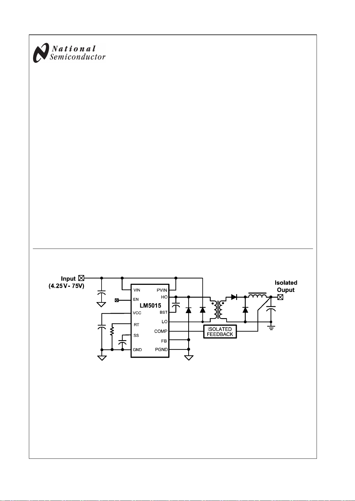
Typical Application Schematic
30034601
© 2007 National Semiconductor Corporation 300346 www.national.com
LM5015 High Voltage Monolithic Two-Switch Forward DC-DC Regulator
Page 2
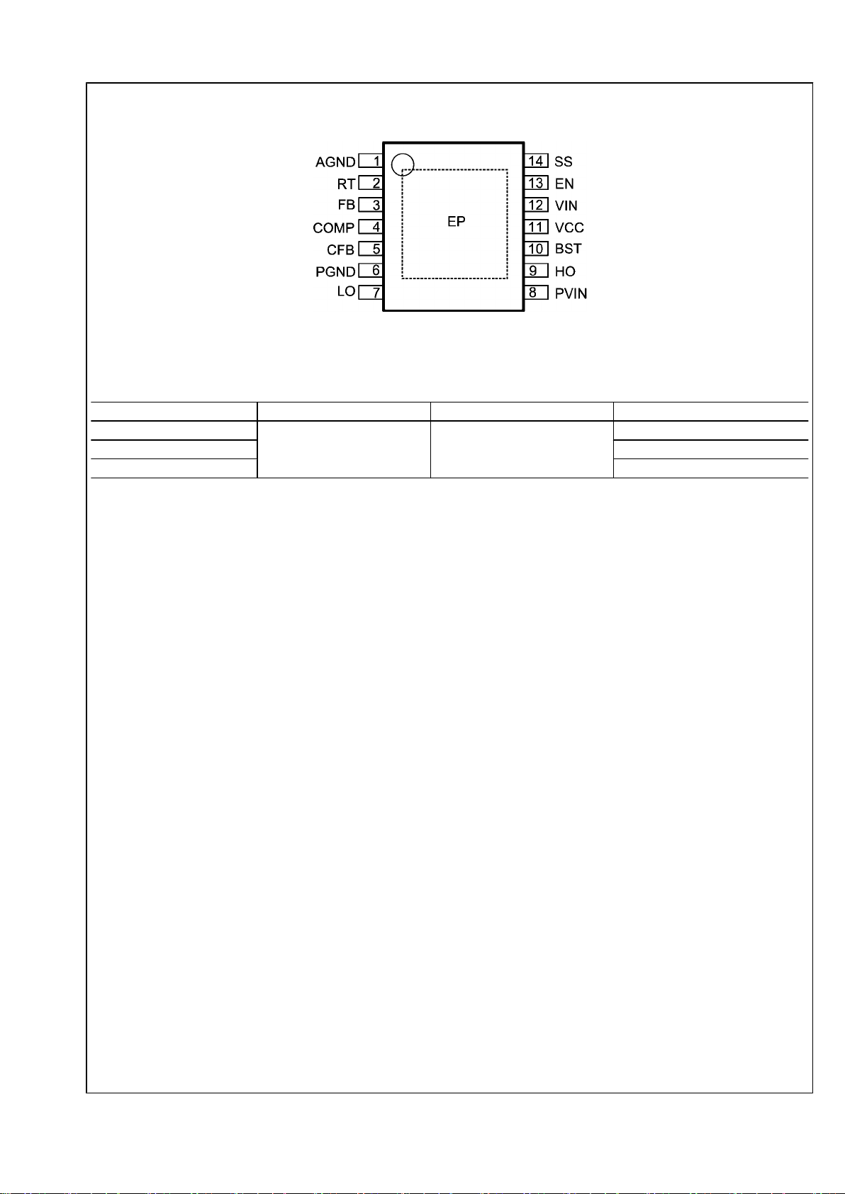
Connection Diagram
30034602
Top View
TSSOP-14 EP Package
Ordering Information
Order Number Package Type NSC Package Drawing Supplied As
LM5015MH
TSSOP-14 EP MXA14A
94 Units per Antistatic Tube
LM5015MHE 250 Units on Tape and Reel
LM5015MHX 2500 Units on Tape and Reel
www.national.com 2
LM5015
Page 3

Pin Descriptions
Pin Name Description Application Information
1 AGND Analog ground Internal reference for the regulator control functions. The AGND pin and
the PGND pin should be connected directly to minimize switching noise and
prevent erratic operation.
2 RT Oscillator frequency
programming and optional
synchronization input
The internal oscillator is set with a resistor between this pin and the AGND
pin. The recommended switching frequency range is 25KHz to 750 kHz.
The RT pin can accept synchronization pulses from an external clock. A
100 pF capacitor is recommended for coupling the synchronizing clock to
the RT pin.
3 FB Feedback input of the internal
error amplifier, for non-isolated
applications
This pin is connected to the inverting input of the internal error amplifier.
The 1.26V reference is internally connected to the non-inverting input of
the error amplifier. In isolated application using an external error amplifier,
this pin should be connected to the AGND pin.
4 COMP Control input for the PWM
comparator
Internally connected to the open drain output of the internal error amplifier.
COMP pull-up is provided by an internal 5 kΩ resistor which may be used
to bias an opto-coupler transistor in isolated applications.
5 CFB Current feedback pin Feedback in put for high bandwidth isolated applications. An NPN current
mirror couples the external opto-coupler current to the PWM comparator
while maintaining a relatively constant opto-coupler voltage.
6 PGND Power ground Internally connected to the current sense resistor in the source of the low
side MOSFET switch.
7 LO Low side switch drain The drain terminal of the internal low side power MOSFET.
8 PVIN Input supply pin for high side
switch
Internally connected to the drain of the high side power MOSFET.
9 HO High side switch source The source terminal of the high side power MOSFET.
10 BST High side bootstrap bias An external capacitor is required between the BST and the HO pins. A
minimum capacitor value of 0.022 µF is recommended. The capacitor is
charged from VCC via an internal diode during the power MOSFET off-time.
11 VCC Bias regulator output, or input for
external bias supply
VCC tracks VIN up to 6.9V. At higher VIN voltages, VCC is regulated to 6.9
Volts. A 0.47µF or greater ceramic decoupling capacitor is required on the
VCC pin. An external bias voltage between 7V and 14V applied to the VCC
pin will disable the internal VCC regulator, reduce internal power
dissipation, and improve the converter efficiency.
12 VIN Analog input voltage pin Power supply Input for the switching regulator control blocks.
13 EN Enable / Under-Voltage Lock-
Out / Shutdown input
An external voltage divider can be used to set the input under-voltage
lockout threshold. If the EN pin is left unconnected, a 6 µA pull-up current
source pulls the EN pin high to enable the regulator.
14 SS Soft-start An internal 11 µA current source charges an external capacitor connected
to the SS pin to soft-start the switching regulator by gradually raising the
COMP pin voltage.
NA EP Exposed Pad Exposed metal pad on the underside of the package. It is recommended to
connect this pad to the PGND and AGND pins, and also to the PC board
ground plane in order to improve heat dissipation.
3 www.national.com
LM5015
Page 4
Absolute Maximum Ratings (Note 1)
If Military/Aerospace specified devices are required,
please contact the National Semiconductor Sales Office/
Distributors for availability and specifications.
VIN to AGND 76V
BST to AGND 90V
PVIN to HO, LO, PGND 76V
HO to PGND (Steady State) -3V to 76V
LO to PGND (Steady State) -0.3V to 76V
BST to VCC 76V
BST to HO 14V
VCC, EN to AGND 14V
COMP, FB, RT, SS to AGND -0.3V to 7V
PGND to AGND -0.3V to +0.3V
CFB Sink Current 10 mA
Maximum Junction Temperature 150°C
Storage Temperature −65°C to + 150°C
ESD Rating
Human Body Model 2 kV
Operating Ratings
V
IN
4.25V to 75V
Operation Junction Temperature −40°C to + 125°C
Electrical Characteristics Limits in standard type are for T
J
= 25°C only; limits in boldface type apply over the
junction temperature (TJ) range of −40°C to + 125°C. Minimum and Maximum limits are guaranteed through test, design, or
statistical correlation. Typical values represent the most likely parametric norm at TJ = 25°C, and are provided for reference
purposes only. V
VIN
= 48V, RRT = 31.6 kΩ unless otherwise stated. See (Note 3).
Symbol Parameters Conditions Min Typ Max Units
STARTUP REGULATOR
V
VCC-REG
VCC Regulator Output 6.35 6.85 7.25 V
VCC Current Limit V
VCC
= 6V 20 25 mA
VCC UVLO Threshold VCC increasing, VIN = VCC, EN=open 3.45 3.75 4.05 V
VCC UVLO Hysteresis VIN = VCC, EN = open 0.15 V
Bias Current (IIN) VFB = 1.5V 3.1 4.5 mA
I
Q
Shutdown Current (IIN) VEN = 0V 110 170 µA
EN THRESHOLDS
EN Shutdown Threshold VEN increasing 0.25 0.45 0.65 V
EN Shutdown Hysteresis 0.1 V
EN Standby Threshold VEN increasing 1.19 1.26 1.3 V
EN Standby Hysteresis 0.1 V
EN Current Source 6 µA
MOSFET CHARACTERSTICS
Low side MOSFET RDS(ON) plus
Current Sense Resistance
ID = 0.6A 0.49 0.93
Ω
MOSFET Leakage Current VLO = 75V 0.05 5 µA
High side MOSFET RDS(ON) ID = 0.6A 0.45 0.90
Ω
MOSFET Leakage Current V
PVIN
= 75V, VHO = PGND 0.05 5 µA
Total Gate Charge including both
Low and High side MOSFETs
V
VCC
= 8V 9 nC
Pre-charge Switch ON Voltage
including series blocking diode
ID = 1 mA 0.82 V
CURRENT LIMIT
I
LIM
Cycle by Cycle Current Limit 1 1.2 1.4 A
Cycle by Cycle Current Limit
Delay
130 ns
OSCILLATOR
F
SW1
Frequency1 RRT = 31.6k 180 200 220 kHz
F
SW2
Frequency2 RRT = 15.4k 365 405 445 kHz
V
RT-SYNC
SYNC Threshold VRT Increasing 3.2 V
SYNC Pulse Width Minimum VRT > V
RT-SYNC
+ 0.5V 15 ns
www.national.com 4
LM5015
Page 5
Symbol Parameters Conditions Min Typ Max Units
PWM COMPARATOR
Maximum Duty Cycle 49 %
Min On-time V
COMP
> V
COMP-OS
140 ns
Min On-time V
COMP
< V
COMP-OS
0 ns
V
COMP-OS
COMP to PWM Comparator
Offset
0.9 1.3 1.55 V
ERROR AMPLIFIER
V
FB-REF
Feedback Reference Voltage Internal reference, VFB = V
COMP
1.236 1.26 1.274 V
FB Bias Current 10 nA
DC Gain 72 dB
COMP Sink Current V
COMP
= 250mV 2 mA
COMP Short Circuit Current VFB = 0, V
COMP
= 0 0.9 1.2 1.5 mA
COMP Open Circuit Voltage VFB = 0 4.5 5.15 5.95 V
COMP to SW Delay 50 ns
Unity Gain Bandwidth 4 MHz
SOFT START
Soft-start Current Source 8 11 14 µA
Soft-start to COMP Offset 0.3 0.5 0.7 V
THERMAL SHUTDOWN
T
SD
Thermal Shutdown Threshold 165 °C
Thermal Shutdown Hysteresis 25 °C
THERMAL RESISTANCE
θ
JC
Junction to Case 6.6 °C/W
θ
JA
Junction to Ambient 40 °C/W
Note 1: Absolute Maximum Ratings are limits beyond which damage to the device may occur. Operating Ratings are conditions under which operation of the
device is intended to be functional. For guaranteed specifications and test conditions, see the Electrical Characteristics.
Note 2: The human body model is a 100pF capacitor discharged through a 1.5 kΩ resistor into each pin. Test Method is per JESD-22-A114.
Note 3: Min and Max limits are 100% production tested at 25°C. Limits over the operating temperature range are guaranteed through correlation using Statistical
Quality Control (SQC) methods. Limits are used to calculate National’s Average Outgoing Quality Level (AOQL).
5 www.national.com
LM5015
Page 6
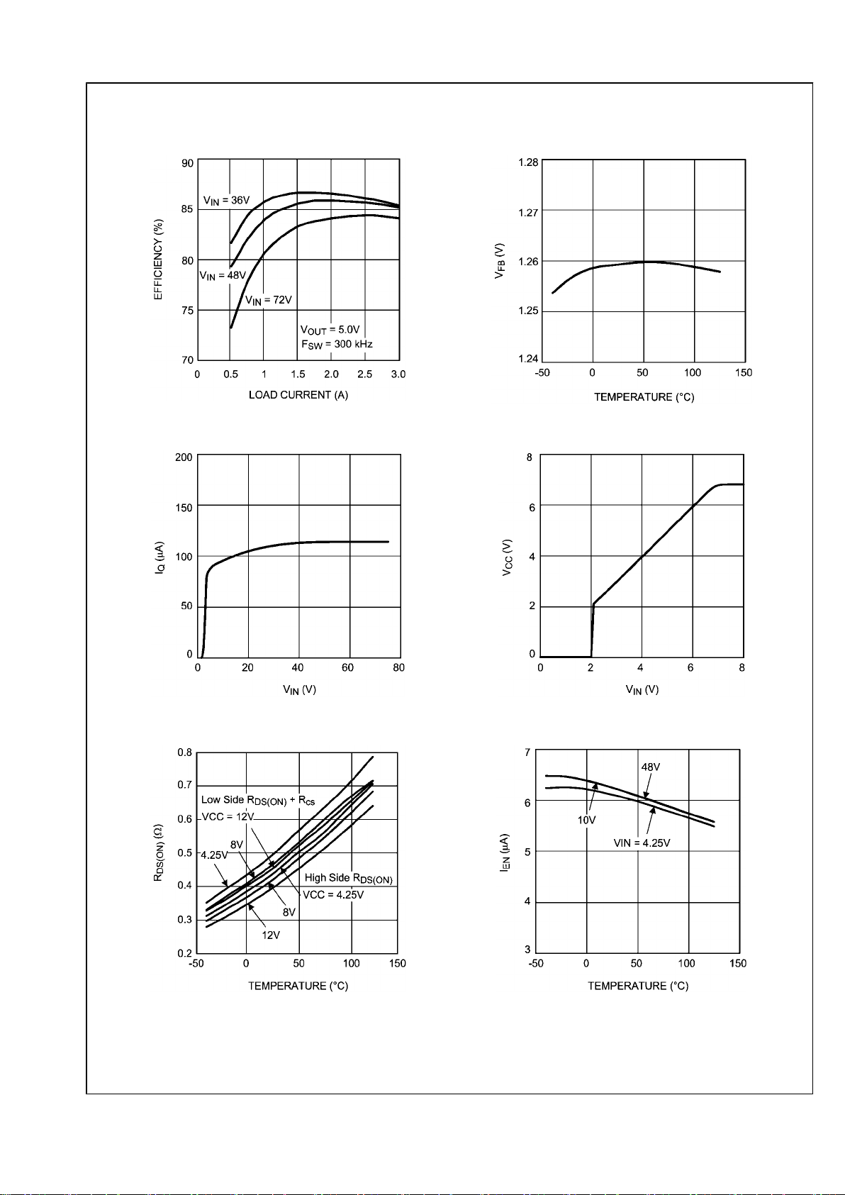
Typical Performance Characteristics
Demo-board Efficiency vs I
OUT
and V
IN
30034603
VFB vs Temperature
30034604
IQ (non-switching) vs VIN
30034605
VCC vs VIN
30034606
RDS(ON) vs VCC vs Temperature
30034607
IEN vs VIN vs Temperature
30034608
www.national.com 6
LM5015
Page 7
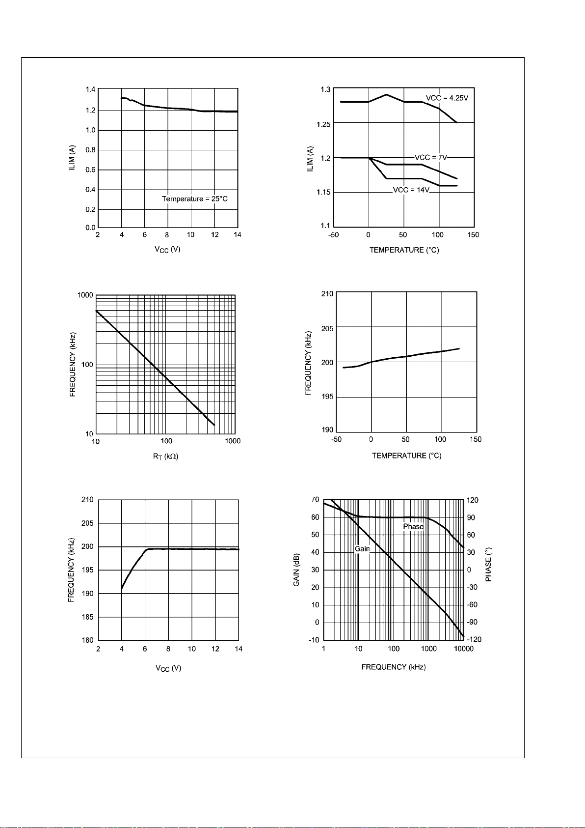
ILIM vs VCC
30034609
ILIM vs VCC vs Temperature
30034610
Fsw vs R
RT
30034611
Fsw vs Temperature
30034612
Fsw vs VCC
30034613
Error Amplifier Gain/Phase
30034614
7 www.national.com
LM5015
Page 8
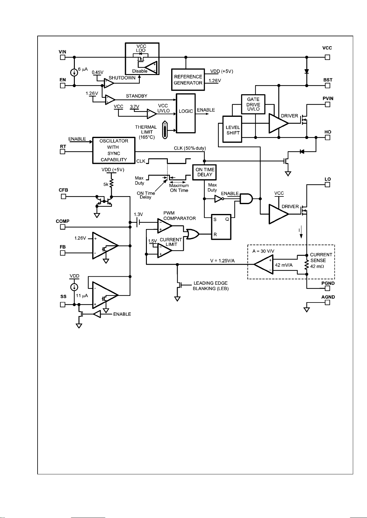
30034615
FIGURE 1. Block Diagram
www.national.com 8
LM5015
Page 9

Functional Description
The LM5015 high voltage switching regulator features all the
functions necessary to implement an efficient power converter using a Two-Switch Forward or Two-Switch Flyback topology. The voltage across the MOSFETs employed in the twoswitch topology is clamped to the input voltage, allowing the
input voltage range to approach the rating of the MOSFETs.
The regulator control method is based upon current mode
control providing cycle-by-cycle current limit, inherent input
voltage feed-forward and simple feedback loop compensation.
Referring to the functional block diagram shown in Figure1,
the operating principle of the LM5015 regulator is as follows:
At the beginning of each switching cycle, the oscillator sets
the driver logic and turns on both the high and low side power
MOSFETs to conduct current through the inductor or power
transformer. The peak current in the MOSFET is controlled
by the voltage at the COMP pin. The COMP voltage, which is
determined by the feedback circuit, is compared with the
sensed current signal of the internal low side power MOSFET.
When the current signal exceeds the COMP voltage, the
PWM comparator resets the driver logic, turning off both power MOSFETs. At the end of the switching cycle the driver logic
is set again by the oscillator to initiate the next switching period.
The LM5015 also contains dedicated circuitry to protect the
IC from abnormal operating conditions. Cycle-by-cycle current limiting prevents the power MOSFET current from exceeding 1 Amp. Thermal Shutdown circuitry holds the driver
logic in reset when the die temperature reaches 165°C, and
returns to normal operation when the die temperature drops
by approximately 25°C. The EN pin can be used as an input
voltage under-voltage lockout (UVLO) during start-up to pre-
vent operation with less than the minimum desired input
voltage.
Bias Input (VIN) and Power Input
(PVIN)
The LM5015 provides two separate input power pins, VIN and
PVIN, allowing for flexible decoupling options. The VIN pin
provides power to the low drop-out VCC bias regulator which
powers all internal control blocks. The PVIN connects directly
to the high side MOSFET drain.
If used with a single input source, the recommended configuration is shown in Figure 2a. Separate input pins allow the
bias input (VIN) to be de-coupled from the main power input
as shown. It is possible to directly connect the VIN and PVIN
pins for applications with localized de-coupling capacitors.
For applications where a lower voltage auxiliary source is
available, the configuration shown in Figure 2b can be used.
Powering the VIN pin with a relatively low voltage auxiliary
source reduces the IC power dissipation and increases the
conversion efficiency, especially when the main power source
for PVIN is relatively large. The VIN and PVIN pins are independent and can be separately biased at any voltages within
the 4.25V to 75V recommended operating range.
In high voltage applications extra care should be taken to ensure that the VIN and PVIN pins do not exceed the Absolute
Maximum Voltage Ratings of 76V. Voltage ringing on the input line during line transients that exceeds the Absolute Maximum Ratings can damage the IC. Both careful PC board
layout and the use of quality bypass capacitors located close
to the VIN and AGND pins, and to the PVIN to PGND pins,
are essential.
30034616
FIGURE 2. Analog and Power Input Ports
9 www.national.com
LM5015
Page 10

The PVIN and PGND pins are internally connected to the high
and low side power MOSFETs, respectively. When designing
the PC board, the input filter capacitor should connect directly
to these pins with short connection traces.
The VIN operating range is 4.25V to 75V. The current drawn
into the VIN pin depends primarily on the gate charge of the
internal power MOSFETs, the switching frequency, and any
external load on the VCC pin. It is recommended that a small
filter shown in Figure 2 be used for the VIN input to suppress
transients which may occur at the input supply. This is particularly important when VIN is operated close to the maximum operating rating of the LM5015.
High Voltage VCC Regulator
The LM5015 VCC Low Drop Out (LDO) regulator allows the
LM5015 to operate at the lowest possible input voltage. When
power is applied to the VIN pin and the EN pin voltage is
greater than 0.45V, the VCC regulator is enabled, supplying
current into the external capacitor connected to the VCC pin.
When the VIN voltage is between 4.25V and 6.9V, the VCC
voltage is approximately equal to the VIN voltage. When the
voltage on the VIN pin exceeds 6.9V, the VCC pin voltage is
regulated at 6.9V. The total input operating range of the VCC
LDO regulator is 4.25V to 75V.
The output of the VCC regulator is current limited to 20mA.
During power-up, the VCC regulator supplies current into the
required decoupling capacitor (0.47 µF or greater ceramic
capacitor) at the VCC pin. When the voltage at the VCC pin
exceeds the VCC UVLO threshold of 3.75V and the EN pin is
greater than 1.26V the PWM controller is enabled and switching begins. The controller remains enabled until VCC falls
below 3.60V or the EN pin falls below 1.16V.
An auxiliary supply voltage can be applied to the VCC pin to
reduce the IC power dissipation. If the auxiliary voltage is
greater than 6.9V, the internal regulator will essentially shutoff, and internal power dissipation will be decreased by the
VIN-VCC voltage difference times the operating current. The
externally applied VCC voltage should not exceed 14V. The
VCC regulator series pass MOSFET includes a body diode
(see Figure 1) between VCC and VIN that should not be forward biased in normal operation. Therefore, the auxiliary VCC
voltage should never exceed the VIN voltage.
High Side Bootstrap Bias
The high side bootstrap bias provides power to drive the high
side power MOSFET. An external capacitor is required between the BST and the HO pins. A minimum capacitor value
of 0.022 µF is recommended. The capacitor is charged from
VCC via an internal diode during each power MOSFET offtime.
Oscillator
A single external resistor connected between RT and AGND
pins sets the LM5015 oscillator frequency. To set a desired
oscillator frequency (FSW), the necessary value for the RT resistor can be calculated from the following equation:
The tolerance of the external resistor and the frequency tolerance indicated in the Electrical Characteristics table must
be taken into account when determining the total variation of
the switching frequency.
External Synchronization
The LM5015 can be synchronized to the rising edge of an
external clock. Because the oscillator uses a divide-by-two
circuit, the switching frequency FSW in the above equation is
actually half the native oscillator frequency. Therefore, in order to synchronize, the external clock must have a frequency
higher than twice the free running FSW set by the RT resistor.
The clock signal should be coupled through a 100 pF capacitor into the RT pin. A peak voltage level greater than 3.2V at
the RT pin is required for detection of the sync pulse. The DC
voltage across the RT resistor is internally regulated at 1.5
volts. The negative portion of the AC voltage of the synchronizing clock is clamped to 1.5V by an amplifier inside the
LM5015 with approximately 100Ω output impedance. Therefore, the AC pulse superimposed on the RT resistor must have
positive pulse amplitude of 1.7V or greater to successfully
synchronize the oscillator. The sync pulse width measured at
the RT pin should have a duration greater than 15 ns and less
than 5% of the switching period. The RT resistor is always
required, whether the oscillator is free running or externally
synchronized. The RT resistor should be located very close to
the device and connected directly to the RT and AGND pins
of the LM5015.
Enable / Standby
The LM5015 contains a dual level Enable circuit. When the
EN pin voltage is below 0.45V, the IC is in a low current shutdown mode with the VCC LDO disabled. When the EN pin
voltage is raised above the 0.45V shutdown threshold but below the 1.26V standby threshold, the VCC LDO regulator is
enabled, while the remainder of the IC is disabled. When the
EN pin voltage is raised above the 1.26V standby threshold,
all functions are enabled and normal operation begins. An internal 6 µA current source pulls up the EN pin to activate the
IC when the EN pin is left disconnected.
An external set-point resistor divider from VIN to AGND can
be used to determine the minimum operating input voltage of
the regulator. The divider must be designed such that the EN
pin exceeds the 1.26V standby threshold when VIN is in the
desired operating range. The internal 6 µA current source
should be included when determining the resistor values. The
shutdown and standby thresholds have 100 mV hysteresis to
prevent noise from toggling between modes. The EN pin is
internally protected by a 6V Zener diode through a 1 kΩ resistor. The enabling voltage may exceed the Zener voltage,
however the Zener current should be limited to less than 4
mA.
Error Amplifier and PWM
Comparator
An internal high gain error amplifier generates an error signal
proportional to the difference between the regulated output
voltage and an internal precision reference. The output of the
error amplifier is connected to the COMP pin allowing the user
to add loop compensation, typically a Type II network, as illustrated in Figure 3. This network creates a pole at the origin
that rolls off the high DC gain of the amplifier, which is necessary to accurately regulate the output voltage. A zero provides phase boost near the open loop unity gain frequency,
and a high frequency pole attenuates switching noise. The
PWM comparator compares the current sense signal from the
current sense amplifier to the error amplifier output voltage at
the COMP pin.
www.national.com 10
LM5015
Page 11

30034618
FIGURE 3. Type II Compensator
When isolation between primary and secondary circuits is required, the Error Amplifier is usually disabled by connecting
the FB pin to AGND. This allows the COMP pin to be driven
directly by the collector of an opto-coupler. In isolated designs
the error amplifier is located on the secondary circuit and
drives the opto-coupler LED. The compensation network is
connected to the secondary side error amplifier. An example
of an isolated regulator with an opto-coupler is shown in Figure 13.
Current Sense Amplifier
The LM5015 employs peak current mode control which also
provides a cycle-by-cycle over current protection feature. An
internal 42 milli-Ohm current sense resistor measures the
current in the low side power MOSFET source. The sense
resistor voltage is amplified 30 times to provide a 1.25V/A
signal into the current limit comparator. Current limiting is initiated if the internal current limit comparator input exceeds the
1.5V threshold, corresponding to 1.2A. When the current limit
comparator is triggered, the HO and LO output pins immediately switches to the high impedance state.
The current sense signal provides the PWM comparator with
a control signal that reaches 1.5V when the MOSFET current
is 1.2A. To prevent erratic operation at low duty cycle, a leading edge blanking circuit attenuates the current sense signal
for 100 ns when the power MOSFET is turned on. When the
MOSFET is initially turned on, current spikes from the power
MOSFET drain-source and gate-source capacitances flow
through the current sense resistor. These transient currents
normally cease within 50 ns with proper selection of rectifier
diodes and proper PC board layout.
Thermal Protection
Internal Thermal Shutdown circuitry is provided to protect the
IC in the event the maximum junction temperature is exceeded. When the 165°C junction temperature threshold is
reached, the regulator is forced into a low power standby
state, disabling all functions except the VCC regulator. Thermal hysteresis allows the IC to cool down by 25°C before it is
re-enabled.
Power MOSFETs
The LM5015 switching regulator includes two N-Channel
MOSFETs each with 450 mΩ nominal on-resistance. The
drain of the high side MOSFET is the PVIN pin, and the source
the HO pin. The drain of the low side MOSFET is the LO pin,
and the source is internally connected to the PGND pin via
the 42 mΩ internal current sense resistor. The on-resistance
of the LM5015 MOSFETs varies with temperature as shown
in the Typical Performance Characteristics graph. The typical
gate charge for each MOSFETs is 4.5 nC which is supplied
from the VCC and BST pins, respectively, when the MOSFETs are turned on.
The maximum duty cycle of the power MOSFETs is limited
less than 50%. This is achieved by an oscillator divide-by-two
circuit with an additional 50 ns of forced off-time introduced
between the CLK and RS Flip-Flop. Consequently, the maximum duty cycle is limited by the following equation:
Duty
Max_Limit
=(0.5 - 50 ns x FSW) x 100%
Where FSW is the switching frequency in Hertz (Hz). The purpose of limiting the maximum duty cycle less than 50% is to
guarantee successful reset of the power transformer in the
Two-Switch Forward converter topology. See applications information below for more detail.
11 www.national.com
LM5015
Page 12

Application Information
The following information is intended to provide guidelines for
the power supply designer using the LM5015.
TWO-SWITCH FORWARD TOPOLOGY
Two-Switch Forward converter, like the conventional SingleSwitch Forward converter, is derived from the Buck converter
topology. The main difference between a Forward converter
and a Buck is that a power transformer is introduced in the
forward converter. The transformer realizes the input-output
isolation, and the turns ratio provides a means to optimize the
duty cycle for the particular input and output voltage requirements of the application.
The Two-Switch Forward converter employs two power MOSFET switches instead of the one switch of the Single-Switch
Forward converter. However the two-switch approach offers
two major advantages over its single-switch counterpart:
1.
The voltage across the power MOSFET switches in a
Two-Switch Forward converter is clamped to the input
voltage, allowing the input voltage range to approach the
rating of the MOSFETs. Whereas, the maximum
operating voltage of a Single-Switch Forward converter
is typically limited to half the MOSFET voltage rating.
2.
The power transformer of a Two-Switch Forward
converter is simpler, and hence costs less, than that of a
Single-Switch Forward converter, because the TwoSwitch converter transformer eliminates the tertiary reset
winding that is normally required in the Single-Switch
converter.
Figure 4 illustrates the Two-Switch Forward converter topology. The power circuit consists of an input capacitor CIN, two
MOSFET switches QH and QL, two clamp diodes DH and DL,
a power transformer T1, two rectifier diodes D1 and D2, an
output inductor LO, and an output capacitor Co. Since the
LM5015 integrates both QH and QL, a low cost Two-Switch
Forward converter can be realized without a need for discrete
power MOSFETs. With a slightly higher cost, the two rectifier
diodes D1 and D2 on the secondary side of the power transformer can be replaced with synchronous rectifier MOSFETs
to improve efficiency in applications with relatively low output
voltage.
30034619
FIGURE 4. Two-Switch Forward Converter Topology
www.national.com 12
LM5015
Page 13

Figure 5 shows the two operating modes of the Two-Switch
Forward converter. During operation, the two MOSFETS are
turned ON and OFF simultaneously. The output voltage is
regulated by modulating the duty cycle of the MOSFETs. The
relationship between the input voltage VIN, output voltage
V
OUT
, duty cycle D, rectifier diode forward drop VF, and trans-
former turns ratio k is defined by the following equation.
When the MOSFETS are turned ON, as shown in Figure 5(a),
the input voltage is applied to the power transformer primary.
The power transformer is magnetized by the application of the
input voltage, and power flows to the secondary side circuit
via transformer coupling. When the MOSFETS are turned
OFF, as shown in Figure 5(b), the power flow to the primary
is cut off. The residual magnetizing inductance of the power
transformer reverses the voltage across the primary winding
and forces the two clamp diodes DH and DL to conduct. This
effectively clamps the MOSFETs voltage to the input voltage,
and applies the input voltage in reversed polarity to the power
transformer primary winding to demagnetize and reset the
transformer.
30034621
FIGURE 5. Operating Modes of Two-Switch Forward Converter
13 www.national.com
LM5015
Page 14

Note that the power transformer primary receives the voltage
of the nearly equal magnitude but opposite polarities during
the ON and OFF period of the power MOSFETs. In order to
guarantee the volt-second balance between the magnetizing
and demagnetizing intervals, the LM5015 limits the maximum
duty cycle less than 50%. Therefore, an LM5015 Two-Switch
Forward regulator always achieves a complete reset of the
power transformer during each switching cycle.
The LM5015 can also be used to implement a Two-Switch
Flyback regulator (Figure 14). The voltage across the MOS-
FETs employed in the Two-Switch Flyback converter is also
clamped to the input voltage, allowing the input voltage range
to approach the rating of the MOSFETs. Generally the Flyback converter is simpler and costs less than the Forward
converter. However, the Flyback converter will have higher
ripple current and voltages, and the conversion efficiency is
typically lower.
www.national.com 14
LM5015
Page 15

EN / UVLO VOLTAGE DIVIDER SELECTION
Two dedicated comparators connected to the EN pin are used
to implement input under-voltage lockout and a shutdown
condition. When the EN pin voltage is below 0.45V, the controller is in a low current shutdown mode where the VIN
current is reduced to 110 µA. For an EN pin voltage greater
than 0.45V but less than 1.26V the controller is in standby
mode, with all internal circuits operational, but with the power
MOSFETs disabled. Once the EN pin voltage is greater than
1.26V, the controller is fully enabled and the HO and LO outputs commence switching. Two external resistors can be
used to program the minimum operational voltage for the
power converter as shown in Figure 6. When the EN pin voltage falls below the 1.26V threshold, an internal 100 mV
threshold hysteresis prevents noise from toggling the state.
Therefore, the voltage at the EN pin must be reduced to 1.16V
to transition to the standby state. Resistance values for R1
and R2 can be determined from the following equations,
where V
PWR
is the desired turn-on voltage and I
DIVIDER
is the
user-defined current through R1 and R2.
For example, if the LM5015 is to be enabled when V
PWR
reaches 16V, I
DIVIDER
could be chosen as 500 µA which would
set R1 to 29.4 kΩ and R2 to 2.49 kΩ. If the voltage at the EN
pin can exceed 6V, then the current into the 6V protection
Zener must be limited below 4 mA by the external resistors.
Be sure to check both the power and voltage rating for the
selected R1 resistor (some 0603 resistors are rated as low as
50V maximum operating voltage).
30034623
FIGURE 6. Basic EN (UVLO) Configuration
A remote enable function can be accomplished with open
drain device(s) connected to the EN pin as shown in Figure
7. A MOSFET or an NPN transistor connected to the EN pin
will force the regulator into the low power ‘off’ state. Adding a
PN diode in the drain (or collector) provides the offset to
achieve the standby state. The advantage of standby is that
the VCC LDO is not disabled and external circuitry powered
by VCC remains functional.
30034624
FIGURE 7. Remote Standby and Disable Control
15 www.national.com
LM5015
Page 16

SOFT-START
Soft-start is implemented with an external capacitor CSS connected to the SS pin as shown in Figure 8. The SS discharge
MOSFET conducts during Shutdown and Standby modes.
When the SS pin is low, the COMP voltage is held below the
PWM offset voltage (1.3V) by the SS buffer amplifier, thus
inhibiting PWM pulses. When the EN pin exceeds the 1.26V
standby threshold, the ENABLE signal will turn-off the SS
discharge MOSFET and allow the internal 11 µA current
source to charge the SS capacitor. The COMP voltage will
follow the SS voltage under the control of the open-drain SS
buffer amplifier. The CSS capacitor will cause the COMP voltage to gradually increase, until the output voltage achieves
regulation, and the error amplifier assumes control of the
COMP and the PWM duty cycle. The CSS capacitor continues
charging by the internal 11 µA current source, preventing the
SS voltage from interfering with the normal error amplifier
function. During shutdown, the SS discharge MOSFET conducts to discharge the CSS capacitor.
30034625
FIGURE 8. Soft-Start
www.national.com 16
LM5015
Page 17

CONVENTIONAL ISOLATED OUTPUT FEEDBACK
DESIGNS
When isolation between the primary and secondary circuits is
required, the internal error amplifier is usually disabled by
connecting the FB pin to AGND, and an external error amplifier is employed on the secondary side of the isolation boundary. An opto-coupler is normally used to send the feedback
signal across the isolation boundary, as shown in Figure 9.
The LM5015 provides built-in pull-up for the collector of the
opto-coupler at the COMP pin through a 5 kΩ internal resistor.
Similar compensation network used in Figure 3 is applicable
to the external, secondary-side error amplifier. The LM431A
shown in Figure 9 provides both the voltage reference and
error amplifier required to regulate the isolated output voltage.
30034626
FIGURE 9. Conventional Isolated Feedback
HIGH BANDWIDTH ISOLATED FEEDBACK DESIGN
USING THE CFB PIN
The LM5015 also includes a current mirror circuit for optional
high bandwidth feedback loop design. As shown in Figure 10,
the emitter of the opto-coupler transistor can be connected to
the CFB pin, and the collector connected to VCC through an
external 1 kΩ resistor. The 1 kΩ resistor to VCC is used to
protect the CFB pin by limiting the opto-coupler current to less
than 10 mA. The 1 kΩ resistor from the opto-coupler collector
to ground is introduced to protect the opto-coupler from excess voltage by limiting its VCE to less than 50% of Vcc max.
When the output voltage is below regulation, no current flows
into the CFB pin and the PWM of the LM5015 operates at
maximum duty cycle.
17 www.national.com
LM5015
Page 18

30034627
FIGURE 10. High bandwidth Isolated Feedback Using CFB Pin
The two external pull-up and pull-down resistors are effectively connected in parallel for ac signal, yielding a collector
resistance on the opto-coupler of 0.5 kΩ. This resistance is
10 times smaller than the internal pull up resistor and the pole
associated with the collector-base capacitance of the optocoupler transistor is pushed out to a decade higher frequency.
Moving the opto-coupler pole to a higher frequency allows
higher loop bandwidth capability than conventional isolated
feedback designs (see Figure 9).
OUTPUT VOLTAGE
Output voltage is normally set with a resistor divider shown in
Figure 11. To set the regulator’s output voltage to VO, the two
resistors must satisfy the following equation:
where V
REF
is the reference voltage of the error amplifier,
which is 1.26V for the LM5015’s internal error amplifier.
30034629
FIGURE 11. Output Voltage Setting
In isolated designs, the reference and error amplifier are located on the secondary side. To obtain a 5V output in an
isolated feedback design using LMV431A (whose nominal
V
REF
is1.24V), the feedback divider resistors ratio specified
by above equation is 0.330. Selecting 24.3 kΩ for RO1, then
RO2 should be 8.06 kΩ. In a similar non-isolated converter
design using the internal error amplifier, the divider’s resistors
ratio is 0.337, therefore if 24.3 kΩ is selected for RO1, then
RO2 should be 8.20 kΩ.
Multiple resistors in series or parallel combinations for either
RO1, or RO2, or both, may be necessary to set a required output voltage. Note that the accuracy of the output voltage
setting is determined by the tolerance of the divider resistors
as well as the accuracy of V
REF
. The accuracy of the LM5015
internal V
REF
is 1.5%, and the most popular chip resistors
have a tolerance of 1%, therefore the achievable output accuracy with the internal error amplifier and 1% resistors is
about 2.5%. To achieve better output voltage accuracy, use
an external voltage reference with higher precision and resistors of tighter tolerance, such as the 0.1%, resistors for
RO1 and RO2.
PRINTED CIRCUIT BOARD LAYOUT
The LM5015 Current Sense and PWM comparators are very
fast and may respond to short duration noise pulses. The
components at the HO, LO, COMP, EN, VCC and the RT pins
should be as physically close as possible to the IC, thereby
minimizing noise pickup on the PC board tracks. The HO and
LO output pins of the LM5015 should have short, wide conductors to the power path inductors, transformers and capacitors in order to minimize parasitic inductance that reduces
efficiency and increases conducted and radiated noise. Ceramic decoupling capacitors are recommended between the
VIN pin to the AGND pin, between the PVIN pin and PGND
pin, and between the VCC pin to the AGND pin. Use short,
direct connections to avoid clock jitter due to ground voltage
differentials. Small package surface mount X7R or X5R capacitors are preferred for high frequency performance and
limited variation over temperature and applied voltage.
If an application using the LM5015 produces high junction
temperatures during normal operation, multiple vias from the
exposed metal pad on the underside of the IC package to a
PC board ground plane will help conduct heat away from the
www.national.com 18
LM5015
Page 19

IC. Judicious positioning of the PC board within the end product, along with use of any available air flow will help reduce
the junction temperature. If using forced air cooling, avoid
placing the LM5015 in the airflow shadow of large components, such as input or output capacitors, inductors or transformers.
Application Examples
The following schematics present four examples dc-dc converters utilizing the LM5015 switching regulator IC:
1.
Non-Isolated Two-Switch Forward for 48V input and 5V
2.5A output,
2.
Isolated Two-Switch Forward for 48V input and 5V 2.5A
output
3.
Isolated Two-Switch Flyback converter for 48V input and
5V 2.5A output,
4.
A 1:1 dc-dc transformer with the input/output operating
range of 5V to 15V
48V NON-ISOLATED TWO-SWITCH FORWARD
The Non-Isolated Two-Switch Forward converter shown in
Figure 12 utilizes the internal voltage reference for the regulation set-point. The output is +5V at 2.5A while the input
voltage can vary from 36V to 72V. The switching frequency is
300 kHz. An auxiliary winding on transformer (T1) provides
10V to power the LM5015 when the output is in regulation.
This disables the internal high voltage VCC LDO regulator
and improves efficiency. The converter can be shut down by
driving the EN input below 1.26V with an open-collector or
open-drain transistor. An external synchronizing frequency
can be applied to the SYNC input.
30034630
FIGURE 12. Non-Isolated Two-Switch Forward
19 www.national.com
LM5015
Page 20

48V ISOLATED TWO-SWITCH FORWARD
The Isolated Two-Switch Forward converter shown in Figure
13 utilizes a 1.24V voltage reference (LMV431A) located on
the isolated secondary side for the regulation set-point. The
LM5015 internal error amplifier is disabled by grounding the
FB pin. The LMV431A controls the current through the opto-
coupler LED, which sets the COMP pin voltage. The output is
+5V at 2.5A and the input voltage ranges from 36V to 72V.
The switching frequency is 300 kHz. The functions of the EN
and SYNC inputs are the same as in the previous example
circuit.
30034631
FIGURE 13. Isolated Two-Switch Forward
ISOLATED TWO-SWITCH FLYBACK
The Isolated Two-Switch Flyback converter shown in Figure
14 utilizes a 1.24V voltage reference (LMV431A) located on
the isolated secondary side for the regulation set-point. The
LM5015 internal error amplifier is disabled by grounding the
FB pin. The LMV431A controls the current through the optocoupler LED, which sets the COMP pin voltage. The output is
+5V at 2.5A and the input voltage ranges from 36V to 72V.
The switching frequency is 300 kHz. The Flyback converter
is less complex than the previous Forward converter example
in Figure 13. However, the Flyback converter produces higher
input and output ripples of voltage and currents, and lower
conversion efficiency by about 2%. The functions of the EN
and SYNC inputs are the same as in the previous example
circuits.
This circuit can be used with the LM5073 for a low cost isolated Power over Ethernet (PoE) Power Device (PD) application that does not require a discrete power MOSFET.
30034632
FIGURE 14. Isolated Two-Switch Flyback
www.national.com 20
LM5015
Page 21

DC-DC TRANSFORMER
The DC-DC transformer shown in Figure 15 provides a 1:1
input voltage to output voltage conversion with ground isolation. The circuit operates in open loop manner operating at
the maximum duty cycle limit of the LM5015. The power
transformer primary-secondary turns ratio is 1:2 (primary to
secondary). Therefore, at the maximum duty cycle of 0.5, the
output voltage will be approximately equal to the input voltage. A Zener diode Z1 is used at the output rail as a simple
means to protect the output against over-voltage under light
and no load conditions. The maximum load of this example
circuit is 0.3A, and the operating voltage range is from 5V to
15V.
30034633
FIGURE 15. DC-DC Transformer
21 www.national.com
LM5015
Page 22

Physical Dimensions inches (millimeters) unless otherwise noted
14-Lead Exposed Pad Package
NS Package Number MXA14A
www.national.com 22
LM5015
Page 23

Notes
23 www.national.com
LM5015
Page 24

Notes
LM5015 High Voltage Monolithic Two-Switch Forward DC-DC Regulator
For more National Semiconductor product information and proven design tools, visit the following Web sites at:
Products Design Support
Amplifiers www.national.com/amplifiers WEBENCH www.national.com/webench
Audio www.national.com/audio Analog University www.national.com/AU
Clock Conditioners www.national.com/timing App Notes www.national.com/appnotes
Data Converters www.national.com/adc Distributors www.national.com/contacts
Displays www.national.com/displays Green Compliance www.national.com/quality/green
Ethernet www.national.com/ethernet Packaging www.national.com/packaging
Interface www.national.com/interface Quality and Reliability www.national.com/quality
LVDS www.national.com/lvds Reference Designs www.national.com/refdesigns
Power Management www.national.com/power Feedback www.national.com/feedback
Switching Regulators www.national.com/switchers
LDOs www.national.com/ldo
LED Lighting www.national.com/led
PowerWise www.national.com/powerwise
Serial Digital Interface (SDI) www.national.com/sdi
Temperature Sensors www.national.com/tempsensors
Wireless (PLL/VCO) www.national.com/wireless
THE CONTENTS OF THIS DOCUMENT ARE PROVIDED IN CONNECTION WITH NATIONAL SEMICONDUCTOR CORPORATION
(“NATIONAL”) PRODUCTS. NATIONAL MAKES NO REPRESENTATIONS OR WARRANTIES WITH RESPECT TO THE ACCURACY
OR COMPLETENESS OF THE CONTENTS OF THIS PUBLICATION AND RESERVES THE RIGHT TO MAKE CHANGES TO
SPECIFICATIONS AND PRODUCT DESCRIPTIONS AT ANY TIME WITHOUT NOTICE. NO LICENSE, WHETHER EXPRESS,
IMPLIED, ARISING BY ESTOPPEL OR OTHERWISE, TO ANY INTELLECTUAL PROPERTY RIGHTS IS GRANTED BY THIS
DOCUMENT.
TESTING AND OTHER QUALITY CONTROLS ARE USED TO THE EXTENT NATIONAL DEEMS NECESSARY TO SUPPORT
NATIONAL’S PRODUCT WARRANTY. EXCEPT WHERE MANDATED BY GOVERNMENT REQUIREMENTS, TESTING OF ALL
PARAMETERS OF EACH PRODUCT IS NOT NECESSARILY PERFORMED. NATIONAL ASSUMES NO LIABILITY FOR
APPLICATIONS ASSISTANCE OR BUYER PRODUCT DESIGN. BUYERS ARE RESPONSIBLE FOR THEIR PRODUCTS AND
APPLICATIONS USING NATIONAL COMPONENTS. PRIOR TO USING OR DISTRIBUTING ANY PRODUCTS THAT INCLUDE
NATIONAL COMPONENTS, BUYERS SHOULD PROVIDE ADEQUATE DESIGN, TESTING AND OPERATING SAFEGUARDS.
EXCEPT AS PROVIDED IN NATIONAL’S TERMS AND CONDITIONS OF SALE FOR SUCH PRODUCTS, NATIONAL ASSUMES NO
LIABILITY WHATSOEVER, AND NATIONAL DISCLAIMS ANY EXPRESS OR IMPLIED WARRANTY RELATING TO THE SALE
AND/OR USE OF NATIONAL PRODUCTS INCLUDING LIABILITY OR WARRANTIES RELATING TO FITNESS FOR A PARTICULAR
PURPOSE, MERCHANTABILITY, OR INFRINGEMENT OF ANY PATENT, COPYRIGHT OR OTHER INTELLECTUAL PROPERTY
RIGHT.
LIFE SUPPORT POLICY
NATIONAL’S PRODUCTS ARE NOT AUTHORIZED FOR USE AS CRITICAL COMPONENTS IN LIFE SUPPORT DEVICES OR
SYSTEMS WITHOUT THE EXPRESS PRIOR WRITTEN APPROVAL OF THE CHIEF EXECUTIVE OFFICER AND GENERAL
COUNSEL OF NATIONAL SEMICONDUCTOR CORPORATION. As used herein:
Life support devices or systems are devices which (a) are intended for surgical implant into the body, or (b) support or sustain life and
whose failure to perform when properly used in accordance with instructions for use provided in the labeling can be reasonably expected
to result in a significant injury to the user. A critical component is any component in a life support device or system whose failure to perform
can be reasonably expected to cause the failure of the life support device or system or to affect its safety or effectiveness.
National Semiconductor and the National Semiconductor logo are registered trademarks of National Semiconductor Corporation. All other
brand or product names may be trademarks or registered trademarks of their respective holders.
Copyright© 2007 National Semiconductor Corporation
For the most current product information visit us at www.national.com
National Semiconductor
Americas Customer
Support Center
Email:
new.feedback@nsc.com
Tel: 1-800-272-9959
National Semiconductor Europe
Customer Support Center
Fax: +49 (0) 180-530-85-86
Email: europe.support@nsc.com
Deutsch Tel: +49 (0) 69 9508 6208
English Tel: +49 (0) 870 24 0 2171
Français Tel: +33 (0) 1 41 91 8790
National Semiconductor Asia
Pacific Customer Support Center
Email: ap.support@nsc.com
National Semiconductor Japan
Customer Support Center
Fax: 81-3-5639-7507
Email: jpn.feedback@nsc.com
Tel: 81-3-5639-7560
www.national.com
 Loading...