

Page 1
LM5000
High Voltage Switch Mode Regulator
General Description
The LM5000 is a monolithic integrated circuit specifically
designed and optimized for flyback, boost or forward power
converter applications. The internal power switch is rated for
a maximum of 80V, with a current limit set to 2A. Protecting
the power switch are current limit and thermal shutdown
circuits. The current mode control scheme provides excellent
rejection of line transients and cycle-by-cycle current limiting.
An external compensation pin and the built-in slope compensation allow the user to optimize the frequency compensation. Other distinctive features include softstart to reduce
stresses during start-up and an external shutdown pin for
remote ON/OFF control. There are two operating frequency
ranges available. The LM5000-3 is pin selectable for either
300kHz (FS Grounded) or 700kHz (FS Open). The
LM5000-6 is pin selectable for either 600kHz (FS Grounded)
or 1.25MHz (FS Open). The device is available in a low
profile 16-lead TSSOP package (available now) or a thermally enhanced 16-lead LLP package (coming in Q3CY03).
Features
n 80V internal switch
n Operating input voltage range of 3.1V to 40V
n Pin selectable operating frequency
300kHz/700kHz (-3)
600kHz/1.25MHz (-6)
n Adjustable output voltage
n External compensation
n Input undervoltage lockout
n Softstart
n Current limit
n Over temperature protection
n External shutdown
n Small 16-Lead TSSOP or 16-Lead LLP package
Applications
n Flyback Regulator
n Forward Regulator
n Boost Regulator
n DSL Modems
n Distributed Power Converters
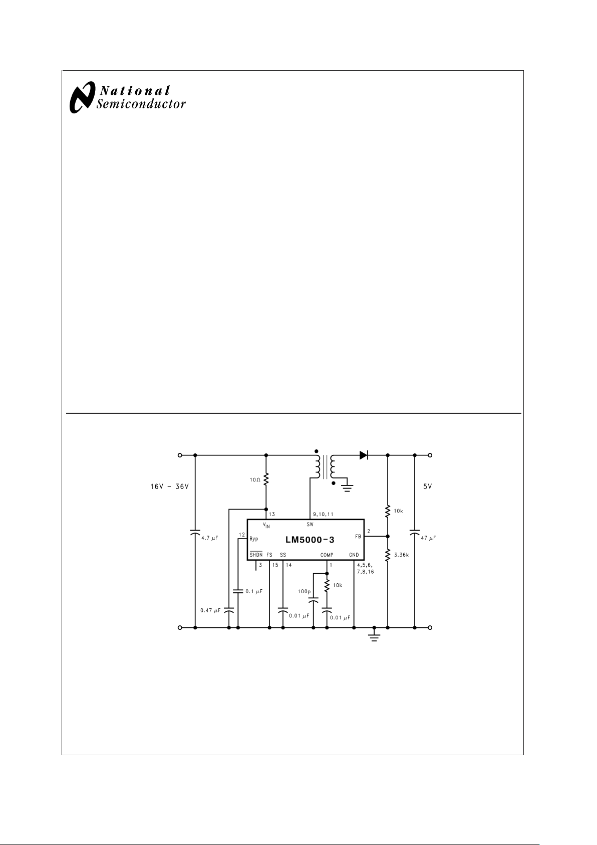
Typical Application Circuit
20031901
LM5000 Flyback Converter
July 2003
LM5000 High Voltage Switch Mode Regulator
© 2003 National Semiconductor Corporation DS200319 www.national.com
Page 2
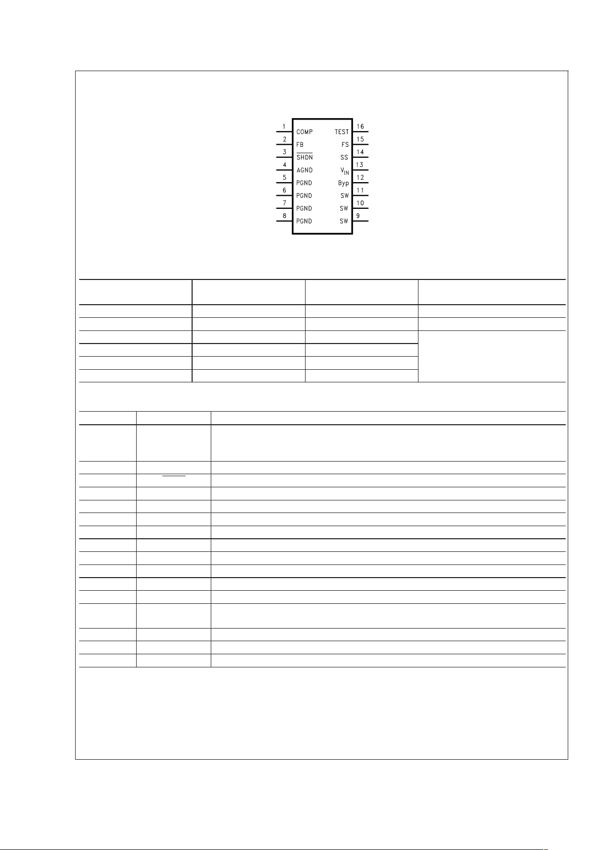
Connection Diagram
Top View
20031904
Ordering Information
Order Number Package Type NSC Package
Drawing
Supplied As
LM5000-3MTC TSSOP-16 MTC16 94 Units, Rail
LM5000-3MTCX TSSOP-16 MTC16 2500 Units, Tape and Reel
LM5000SD-3 LLP-16 SDA16
Coming in Q3CY03
LM5000SDX-3 LLP-16 SDA16
LM5000SD-6 LLP-16 SDA16
LM5000SDX-6 LLP-16 SDA16
Pin Description
Pin Name Function
1 COMP Compensation network connection. Connected to the output of the voltage error amplifier.
The RC compenstion network should be connected from this pin to AGND. An additional
100pF high frequency capacitor to AGND is recommended.
2 FB Output voltage feedback input.
3 SHDN
Shutdown control input, Open = enable, Ground = disable.
4 AGND Analog ground, connect directly to PGND.
5 PGND Power ground.
6 PGND Power ground.
7 PGND Power ground.
8 PGND Power ground.
9 SW Power switch input. Switch connected between SW pins and PGND pins
10 SW Power switch input. Switch connected between SW pins and PGND pins
11 SW Power switch input. Switch connected between SW pins and PGND pins
12 BYP Bypass-Decouple Capacitor Connection, 0.1µF ceramic capacitor recommended.
13 V
IN
Analog power input. A small RC filter is recommended, to suppress line glitches. Typical
values of 10Ω and ≥ 0.1µF are recommended.
14 SS Softstart Input. External capacitor and internal current source sets the softstart time.
15 FS Switching frequency select input. Open = F
high
. Ground = F
low
16 TEST Factory test pin, connect to ground.
LM5000
www.national.com 2
Page 3
Absolute Maximum Ratings (Note 1)
If Military/Aerospace specified devices are required,
please contact the National Semiconductor Sales Office/
Distributors for availability and specifications.
V
IN
-0.3V to 40V
SW Voltage -0.3V to 80V
FB Voltage -0.3V to 5V
COMP Voltage -0.3V to 3V
All Other Pins -0.3V to 7V
Maximum Junction Temperature 150˚C
Power Dissipation(Note 2) Internally Limited
Lead Temperature 216˚C
Infrared (15 sec.) 235˚C
ESD Susceptibility (Note 3)
Human Body Model 2kV
Machine Model 200V
Storage Temperature −65˚C to +150˚C
Operating Conditions
Operating Junction
Temperature Range
(Note 7) −40˚C to +125˚C
Supply Voltage (Note 7) 3.1V to 40V
Electrical Characteristics
Specifications in standard type face are for TJ= 25˚C and those with boldface type apply over the full Operating Temperature Range (T
J
= −40˚C to +125˚C) Unless otherwise specified. VIN= 12V and IL= 0A, unless otherwise specified.
Symbol Parameter Conditions
Min
(Note 4)
Typ
(Note 5)
Max
(Note 4)
Units
I
Q
Quiescent Current FB = 2V (Not Switching)
FS=0V
2.0 2.5 mA
FB = 2V (Not Switching)
FS = Open
2.1 2.5 mA
V
SHDN
=0V 18 30 µA
V
FB
Feedback Voltage 1.2330 1.259 1.2840 V
I
CL
Switch Current Limit 1.35 2.0 2.7 A
%V
FB
/∆VINFeedback Voltage Line
Regulation
3.1V ≤ VIN≤ 40V 0.001 0.04 %/V
I
B
FB Pin Bias Current (Note 6) 55 200 nA
BV Output Switch Breakdown
Voltage
T
J
= 25˚C, ISW= 0.1µA 80 V
T
J
= -40˚C to + 125˚C, ISW=
0.5µA
76
V
IN
Input Voltage Range 3.1 40 V
g
m
Error Amp Transconductance ∆I = 5µA 150 410 750 µmho
A
V
Error Amp Voltage Gain 280 V/V
D
MAX
Maximum Duty Cycle
LM5000-3
FS=0V 85 90 %
Maximum Duty Cycle
LM5000-6
FS = 0V TBD 90 %
T
MIN
Minimum On Time 165 ns
f
S
Switching Frequency
LM5000-3
FS=0V 240 300 360
kHz
FS = Open 550 700 840
Switching Frequency
LM5000-6
FS=0V TBD 600 TBD
FS = Open TBD 1.25 TBD MHz
I
SHDN
Shutdown Pin Current V
SHDN
=0V −1 -2 µA
I
L
Switch Leakage Current VSW= 80V 0.008 5 µA
R
DSON
Switch R
DSON
ISW= 1A 160 445 mΩ
Th
SHDN
SHDN Threshold Output High 0.9 0.6 V
Output Low 0.6 0.3 V
UVLO On Threshold 2.74 2.92 3.10 V
Off Threshold 2.60 2. 77 2.96 V
OVP V
COMP
Trip 0.67 V
I
SS
Softstart Current 8 11 14 µA
LM5000
www.national.com3
Page 4
Electrical Characteristics (Continued)
Specifications in standard type face are for TJ= 25˚C and those with boldface type apply over the full Operating Temperature Range (T
J
= −40˚C to +125˚C) Unless otherwise specified. VIN= 12V and IL= 0A, unless otherwise specified.
Symbol Parameter Conditions
Min
(Note 4)
Typ
(Note 5)
Max
(Note 4)
Units
θ
JA
Thermal Resistance TSSOP, Package only 150 ˚C/W
LLP, Package only 45
Note 1: Absolute maximum ratings are limits beyond which damage to the device may occur. Operating Ratings are conditions for which the device is intended to
be functional, but device parameter specifications may not be guaranteed. For guaranteed specifications and test conditions, see the Electrical Characteristics.
Note 2: The maximum allowable power dissipation is a function of the maximum junction temperature, T
J
(MAX), the junction-to-ambient thermal resistance, θJA,
and the ambient temperature, T
A
. See the Electrical Characteristics table for the thermal resistance of various layouts. The maximum allowable power dissipation
at any ambient temperature is calculated using: P
D
(MAX) = (T
J(MAX)−TA
)/θJA. Exceeding the maximum allowable power dissipation will cause excessive die
temperature, and the regulator will go into thermal shutdown.
Note 3: The human body model is a 100 pF capacitor discharged through a 1.5kΩ resistor into each pin. The machine model is a 200pF capacitor discharged
directly into each pin.
Note 4: All limits guaranteed at room temperature (standard typeface) and at temperature extremes (bold typeface). All room temperature limits are 100%
production tested. All limits at temperature extremes are guaranteed via correlation using standard Statistical Quality Control (SQC) methods. All limits are used to
calculate Average Outgoing Quality Level (AOQL).
Note 5: Typical numbers are at 25˚C and represent the most likely norm.
Note 6: Bias current flows into FB pin.
Note 7: Supply voltage, bias current product will result in aditional device power dissipation. This power may be significant. The thermal dissipation design should
take this into account.
LM5000
www.national.com 4
Page 5
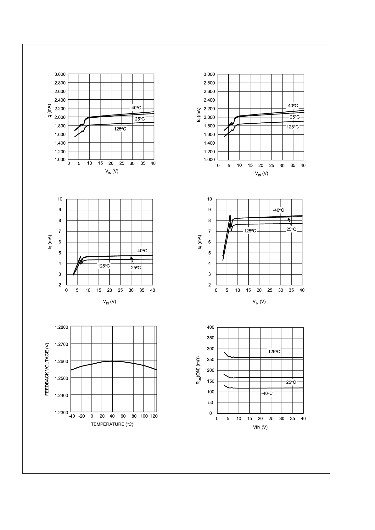
Typical Performance Characteristics
Iq (non-switching) vs V
IN
@
fSW= 300kHz Iq (non-switching) vs V
IN
@
fSW= 700kHz
20031920
20031921
Iq (switching) vs V
IN
@
fSW= 300kHz Iq (switching) vs V
IN
@
fSW= 700kHz
20031922 20031923
Vfbvs Temperature R
DS(ON)
vs V
IN
@
ISW=1A
20031924
20031925
LM5000
www.national.com5
Page 6
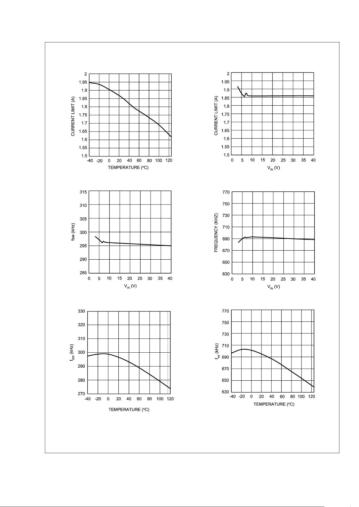
Typical Performance Characteristics (Continued)
Current Limit vs Temperature Current Limit vs V
IN
20031926
20031927
fSWvs. V
IN
@
FS = Low (-3) fSWvs. V
IN
@
FS = High (-3)
20031928
20031929
fSWvs. Temperature@FS = Low (-3) fSWvs. Temperature@FS = High (-3)
20031930
20031931
LM5000
www.national.com 6
Page 7

Typical Performance Characteristics (Continued)
Error Amp. Transconductance vs Temp. BYP Pin Voltage vs V
IN
20031932
20031933
LM5000
www.national.com7
Page 8

20031953
FIGURE 1. 300 kHz operation, 48V output
20031954
FIGURE 2. 700 kHz operation, 48V output
LM5000
www.national.com 8
Page 9

Block Diagram
20031903
Boost Regulator Operation
The LM5000 utilizes a PWM control scheme to regulate the
output voltage over all load conditions. The operation can
best be understood referring to the block diagram and Figure
3. At the start of each cycle, the oscillator sets the driver logic
and turns on the NMOS power device conducting current
through the inductor, cycle 1 of Figure 3 (a). During this
cycle, the voltage at the COMP pin controls the peak inductor current. The COMP voltage will increase with larger loads
and decrease with smaller. This voltage is compared with the
summation of the SW volatge and the ramp compensation.The ramp compensation is used in PWM architectures to
eliminate the sub-harmonic oscillations that occur during
duty cycles greater than 50%. Once the summation of the
ramp compensation and switch voltage equals the COMP
voltage, the PWM comparator resets the driver logic turning
off the NMOS power device. The inductor current then flows
through the output diode to the load and output capacitor,
cycle 2 of Figure 3 (b). The NMOS power device is then set
by the oscillator at the end of the period and current flows
through the inductor once again.
The LM5000 has dedicated protection circuitry running during the normal operation to protect the IC. The Thermal
Shutdown circuitry turns off the NMOS power device when
the die temperature reaches excessive levels. The UVP
comparator protects the NMOS power device during supply
power startup and shutdown to prevent operation at voltages
less than the minimum input voltage. The OVP comparator is
used to prevent the output voltage from rising at no loads
allowing full PWM operation over all load conditions. The
LM5000 also features a shutdown mode. An external capacitor sets the softstart time by limiting the error amp output
range, as the capacitor charges up via an internal 10µA
current source.
The LM5000 is available in two operating frequency ranges.
The LM5000-3 is pin selectable for either 300kHz (FS
Grounded) or 700kHz (FS Open). The LM5000-6 is pin
selectable for either 600kHz (FS Grounded) or 1.25MHz (FS
Open)
LM5000
www.national.com9
Page 10

Operation
CONTINUOUS CONDUCTION MODE
The LM5000 is a current-mode, PWM regulator. When used
as a boost regulator the input voltage is stepped up to a
higher output voltage. In continuous conduction mode (when
the inductor current never reaches zero at steady state), the
boost regulator operates in two cycles.
In the first cycle of operation, shown in Figure 3 (a), the
transistor is closed and the diode is reverse biased. Energy
is collected in the inductor and the load current is supplied by
C
OUT
.
The second cycle is shown in Figure 3 (b). During this cycle,
the transistor is open and the diode is forward biased. The
energy stored in the inductor is transferred to the load and
output capacitor.
The ratio of these two cycles determines the output voltage.
The output voltage is defined approximately as:
where D is the duty cycle of the switch, D and D' will be
required for design calculations.
SETTING THE OUTPUT VOLTAGE
The output voltage is set using the feedback pin and a
resistor divider connected to the output as shown in Figure 1.
The feedback pin is always at 1.259V, so the ratio of the
feedback resistors sets the output voltage.
INTRODUCTION TO COMPENSATION
20031902
FIGURE 3. Simplified Boost Converter Diagram
(a) First Cycle of Operation (b) Second Cycle Of Operation
20031905
FIGURE 4. (a) Inductor current. (b) Diode current.
LM5000
www.national.com 10
Page 11

Operation (Continued)
The LM5000 is a current mode PWM regulator. The signal
flow of this control scheme has two feedback loops, one that
senses switch current and one that senses output voltage.
To keep a current programmed control converter stable
above duty cycles of 50%, the inductor must meet certain
criteria. The inductor, along with input and output voltage,
will determine the slope of the current through the inductor
(see Figure 4 (a)). If the slope of the inductor current is too
great, the circuit will be unstable above duty cycles of 50%.
The LM5000 provides a compensation pin (COMP) to customize the voltage loop feedback. It is recommended that a
series combination of R
C
and CCbe used for the compensation network, as shown in Figure 1. The series combination of R
C
and CCintroduces pole-zero pair according to the
following equations:
where ROis the output impedance of the error amplifier,
850kΩ. For most applications, performance can be optimized by choosing values within the range 5kΩ≤R
C
≤ 20kΩ
and 680pF ≤ C
C
≤ 4.7nF.
COMPENSATION
This section will present a general design procedure to help
insure a stable and operational circuit. The designs in this
datasheet are optimized for particular requirements. If different conversions are required, some of the components may
need to be changed to ensure stability. Below is a set of
general guidelines in designing a stable circuit for continuous conduction operation (loads greater than 100mA), in
most all cases this will provide for stability during discontinuous operation as well. The power components and their
effects will be determined first, then the compensation components will be chosen to produce stability.
INDUCTOR SELECTION
To ensure stability at duty cycles above 50%, the inductor
must have some minimum value determined by the minimum input voltage and the maximum output voltage. This
equation is:
where fs is the switching frequency, D is the duty cycle, and
R
DSON
is the ON resistance of the internal switch. This
equation is only good for duty cycles greater than 50%
(D
>
0.5).
The inductor ripple current is important for a few reasons.
One reason is because the peak switch current will be the
average inductor current (input current) plus ∆i
L
. Care must
be taken to make sure that the switch will not reach its
current limit during normal operation. The inductor must also
be sized accordingly. It should have a saturation current
rating higher than the peak inductor current expected. The
output voltage ripple is also affected by the total ripple current.
DC GAIN AND OPEN-LOOP GAIN
Since the control stage of the converter forms a complete
feedback loop with the power components, it forms a closedloop system that must be stabilized to avoid positive feedback and instability. A value for open-loop DC gain will be
required, from which you can calculate, or place, poles and
zeros to determine the crossover frequency and the phase
margin. A high phase margin (greater than 45˚) is desired for
the best stability and transient response. For the purpose of
stabilizing the LM5000, choosing a crossover point well below where the right half plane zero is located will ensure
sufficient phase margin. A discussion of the right half plane
zero and checking the crossover using the DC gain will
follow.
OUTPUT CAPACITOR SELECTION
The choice of output capacitors is somewhat more arbitrary.
It is recommended that low ESR (Equivalent Series Resistance, denoted R
ESR
) capacitors be used such as ceramic,
polymer electrolytic, or low ESR tantalum. Higher ESR capacitors may be used but will require more compensation
which will be explained later on in the section. The ESR is
also important because it determines the output voltage
ripple according to the approximate equation:
∆V
OUT
) 2∆iLR
ESR
(in Volts)
After choosing the output capacitor you can determine a
pole-zero pair introduced into the control loop by the following equations:
Where RLis the minimum load resistance corresponding to
the maximum load current. The zero created by the ESR of
the output capacitor is generally very high frequency if the
ESR is small. If low ESR capacitors are used it can be
neglected. If higher ESR capacitors are used see the High
Output Capacitor ESR Compensation section.
RIGHT HALF PLANE ZERO
A current mode control boost regulator has an inherent right
half plane zero (RHP zero). This zero has the effect of a zero
in the gain plot, causing an imposed +20dB/decade on the
rolloff, but has the effect of a pole in the phase, subtracting
another 90˚ in the phase plot. This can cause undesirable
effects if the control loop is influenced by this zero. To ensure
the RHP zero does not cause instability issues, the control
loop should be designed to have a bandwidth of
1
⁄2the
frequency of the RHP zero or less. This zero occurs at a
frequency of:
LM5000
www.national.com11
Page 12

Operation (Continued)
where I
LOAD
is the maximum load current.
SELECTING THE COMPENSATION COMPONENTS
The first step in selecting the compensation components R
C
and CCis to set a dominant low frequency pole in the control
loop. Simply choose values for R
C
and CCwithin the ranges
given in the Introduction to Compensation section to set this
pole in the area of 10Hz to 100Hz. The frequency of the pole
created is determined by the equation:
where ROis the output impedance of the error amplifier,
850kΩ. Since R
C
is generally much less than RO, it does not
have much effect on the above equation and can be neglected until a value is chosen to set the zero f
ZC.fZC
is
created to cancel out the pole created by the output capacitor, f
P1
. The output capacitor pole will shift with different load
currents as shown by the equation, so setting the zero is not
exact. Determine the range of f
P1
over the expected loads
and then set the zero f
ZC
to a point approximately in the
middle. The frequency of this zero is determined by:
Now RCcan be chosen with the selected value for CC.
Check to make sure that the pole f
PC
is still in the 10Hz to
100Hz range, change each value slightly if needed to ensure
both component values are in the recommended range. After
checking the design at the end of this section, these values
can be changed a little more to optimize performance if
desired. This is best done in the lab on a bench, checking the
load step response with different values until the ringing and
overshoot on the output voltage at the edge of the load steps
is minimal. This should produce a stable, high performance
circuit. For improved transient response, higher values of R
C
(within the range of values) should be chosen. This will
improve the overall bandwidth which makes the regulator
respond more quickly to transients. If more detail is required,
or the most optimal performance is desired, refer to a more
in depth discussion of compensating current mode DC/DC
switching regulators.
HIGH OUTPUT CAPACITOR ESR COMPENSATION
When using an output capacitor with a high ESR value, or
just to improve the overall phase margin of the control loop,
another pole may be introduced to cancel the zero created
by the ESR. This is accomplished by adding another capacitor, C
C2
, directly from the compensation pin VCto ground, in
parallel with the series combination of R
C
and CC. The pole
should be placed at the same frequency as f
Z1
, the ESR
zero. The equation for this pole follows:
To ensure this equation is valid, and that CC2can be used
without negatively impacting the effects of R
C
and CC,f
PC2
must be greater than 10fPC.
CHECKING THE DESIGN
The final step is to check the design. This is to ensure a
bandwidth of
1
⁄2or less of the frequency of the RHP zero.
This is done by calculating the open-loop DC gain, A
DC
. After
this value is known, you can calculate the crossover visually
by placing a −20dB/decade slope at each pole, and a +20dB/
decade slope for each zero. The point at which the gain plot
crosses unity gain, or 0dB, is the crossover frequency. If the
crossover frequency is at less than
1
⁄2the RHP zero, the
phase margin should be high enough for stability. The phase
margin can also be improved some by adding C
C2
as dis-
cussed earlier in the section. The equation for A
DC
is given
below with additional equations required for the calculation:
mc ) 0.072fs (in A/s)
where RLis the minimum load resistance, VINis the maximum input voltage, and R
DSON
is the value chosen from the
graph "R
DSON
vs. VIN"intheTypical Performance Charac-
teristics section.
SWITCH VOLTAGE LIMITS
In a flyback regulator, the maximum steady-state voltage
appearing at the switch, when it is off, is set by the transformer turns ratio, N, the output voltage, V
OUT
, and the
maximum input voltage, V
IN
(Max):
V
SW(OFF)
=VIN(Max) + (V
OUT+VF
)/N
where V
F
is the forward biased voltage of the output diode,
and is typically 0.5V for Schottky diodes and 0.8V for ultrafast recovery diodes. In certain circuits, there exists a voltage spike, V
LL
, superimposed on top of the steady-state
voltage . Usually, this voltage spike is caused by the transformer leakage inductance and/or the output rectifier recovery time. To “clamp” the voltage at the switch from exceeding
its maximum value, a transient suppressor in series with a
diode is inserted across the transformer primary.
If poor circuit layout techniques are used, negative voltage
transients may appear on the Switch pin. Applying a negative voltage (with respect to the IC’s ground) to any monolithic IC pin causes erratic and unpredictable operation of
that IC. This holds true for the LM5000 IC as well. When
used in a flyback regulator, the voltage at the Switch pin can
go negative when the switch turns on. The “ringing” voltage
LM5000
www.national.com 12
Page 13

Operation (Continued)
at the switch pin is caused by the output diode capacitance
and the transformer leakage inductance forming a resonant
circuit at the secondary(ies). The resonant circuit generates
the “ringing” voltage, which gets reflected back through the
transformer to the switch pin. There are two common methods to avoid this problem. One is to add an RC snubber
around the output rectifier(s). The values of the resistor and
the capacitor must be chosen so that the voltage at the
Switch pin does not drop below −0.4V. The resistor may
range in value between 10Ω and1kΩ, and the capacitor will
vary from 0.001 µF to 0.1 µF. Adding a snubber will (slightly)
reduce the efficiency of the overall circuit.
The other method to reduce or eliminate the “ringing” is to
insert a Schottky diode clamp between the SW pin and the
PGND pin. The reverse voltage rating of the diode must be
greater than the switch off voltage.
OUTPUT VOLTAGE LIMITATIONS
The maximum output voltage of a boost regulator is the
maximum switch voltage minus a diode drop. In a flyback
regulator, the maximum output voltage is determined by the
turns ratio, N, and the duty cycle, D, by the equation:
V
OUT
≈ NxVINxD/(1−D)
The duty cycle of a flyback regulator is determined by the
following equation:
Theoretically, the maximum output voltage can be as large
as desired — just keep increasing the turns ratio of the transformer. However, there exists some physical limitations that
prevent the turns ratio, and thus the output voltage, from
increasing to infinity. The physical limitations are capaci-
tances and inductances in the LM5000 switch, the output
diode(s), and the transformer — such as reverse recovery
time of the output diode (mentioned above).
INPUT LINE CONDITIONING
A small, low-pass RC filter should be used at the input pin of
the LM5000 if the input voltage has an unusually large
amount of transient noise. Additionally, the RC filter can
reduce the dissipation within the device when the input
voltage is high.
Flyback Regulator Operation
The LM5000 is ideally suited for use in the flyback regulator
topology. The flyback regulator can produce a single output
voltage, or multiple output voltages.
The operation of a flyback regulator is as follows: When the
switch is on, current flows through the primary winding of the
transformer, T1, storing energy in the magnetic field of the
transformer. Note that the primary and secondary windings
are out of phase, so no current flows through the secondary
when current flows through the primary. When the switch
turns off, the magnetic field collapses, reversing the voltage
polarity of the primary and secondary windings. Now rectifier
D5 is forward biased and current flows through it, releasing
the energy stored in the transformer. This produces voltage
at the output.
The output voltage is controlled by modulating the peak
switch current. This is done by feeding back a portion of the
output voltage to the error amp, which amplifies the difference between the feedback voltage and a 1.259V reference.
The error amp output voltage is compared to a ramp voltage
proportional to the switch current (i.e., inductor current during the switch on time). The comparator terminates the
switch on time when the two voltages are equal, thereby
controlling the peak switch current to maintain a constant
output voltage.
LM5000
www.national.com13
Page 14

Flyback Regulator Operation (Continued)
ITEM PART NUMBER DESCRIPTION VALUE
C 1 C4532X7R2A105MT Capacitor, CER, TDK 1µ, 100V
C 2 C4532X7R2A105MT Capacitor, CER, TDK 1µ, 100V
C 3 C1206C224K5RAC Capacitor, CER, KEMET 0.22µ, 50V
C 4 C1206C104K5RAC Capacitor, CER, KEMET 0.1µ, 50V
C 5 C1206C104K5RAC Capacitor, CER, KEMET 0.1µ, 50V
C 6 C1206C101K1GAC Capacitor, CER, KEMET 100p, 100V
C 7 C1206C104K5RAC Capacitor, CER, KEMET 0.1µ, 50V
C 8 C4532X7S0G686M Capacitor, CER, TDK 68µ, 4V
C 9 C4532X7S0G686M Capacitor, CER, TDK 68µ, 4V
C 10 C1206C221K1GAC Capacitor, CER, KEMET 220p, 100V
C 11 C1206C102K5RAC Capacitor, CER, KEMET 1000p, 500V
D 1 BZX84C10-NSA Central, 10V Zener, SOT-23
D 2 CMZ5930B-NSA Central, 16V Zener, SMA
D 3 CMPD914-NSA Central, Switching, SOT-23
D 4 CMPD914-NSA Central, Switching, SOT-23
D 5 CMSH3-40L-NSA Central, Schottky, SMC
20031972
FIGURE 5. LM5000 Flyback Converter
LM5000
www.national.com 14
Page 15

ITEM PART NUMBER DESCRIPTION VALUE
T 1 A0009-A Coilcraft, Transformer
R 1 CRCW12064992F Resistor 49.9K
R 2 CRCW12061001F Resistor 1K
R 3 CRCW12061002F Resistor 10K
R 4 CRCW12066191F Resistor 6.19K
R 5 CRCW120610R0F Resistor 10
R 6 CRCW12062003F Resistor 200K
R 7 CRCW12061002F Resistor 10K
Q 1 CXT5551-NSA Central, NPN, 180V
U 1 LM5000-3 Regulator, National
LM5000
www.national.com15
Page 16

Physical Dimensions inches (millimeters)
unless otherwise noted
TSSOP-16 Pin Package (MTC)
For Ordering, Refer to Ordering Information Table
NS Package Number MTC16
LLP-16 Pin Package (SDA)
For Ordering, Refer to Ordering Information Table
NS Package Number SDA16A
LM5000
www.national.com 16
Page 17

Notes
LIFE SUPPORT POLICY
NATIONAL’S PRODUCTS ARE NOT AUTHORIZED FOR USE AS CRITICAL COMPONENTS IN LIFE SUPPORT
DEVICES OR SYSTEMS WITHOUT THE EXPRESS WRITTEN APPROVAL OF THE PRESIDENT AND GENERAL
COUNSEL OF NATIONAL SEMICONDUCTOR CORPORATION. As used herein:
1. Life support devices or systems are devices or
systems which, (a) are intended for surgical implant
into the body, or (b) support or sustain life, and
whose failure to perform when properly used in
accordance with instructions for use provided in the
labeling, can be reasonably expected to result in a
significant injury to the user.
2. A critical component is any component of a life
support device or system whose failure to perform
can be reasonably expected to cause the failure of
the life support device or system, or to affect its
safety or effectiveness.
National Semiconductor
Americas Customer
Support Center
Email: new.feedback@nsc.com
Tel: 1-800-272-9959
National Semiconductor
Europe Customer Support Center
Fax: +49 (0) 180-530 85 86
Email: europe.support@nsc.com
Deutsch Tel: +49 (0) 69 9508 6208
English Tel: +44 (0) 870 24 0 2171
Français Tel: +33 (0) 1 41 91 8790
National Semiconductor
Asia Pacific Customer
Support Center
Email: ap.support@nsc.com
National Semiconductor
Japan Customer Support Center
Fax: 81-3-5639-7507
Email: jpn.feedback@nsc.com
Tel: 81-3-5639-7560
www.national.com
LM5000 High Voltage Switch Mode Regulator
National does not assume any responsibility for use of any circuitry described, no circuit patent licenses are implied and National reserves the right at any time without notice to change said circuitry and specifications.
 Loading...