

Page 1
TL/H/10056
LM494 Pulse Width Modulated Control Circuit
June 1989
LM494
Pulse Width Modulated Control Circuit
General Description
The LM494 is a monolithic integrated circuit which includes
all the necessary building blocks for the design of pulse
width modulated (PWM) switching power supplies, including
push-pull, bridge and series configurations. The device can
operate at switching frequencies between 1.0 kHz and
300 kHz and output voltages up to 40V. The operating temperature range specified for the LM494C is 0
§
Cto70§C and
for the LM494V is
b
40§Ctoa85§C.
Features
Y
Uncommitted output transistors capable of 200 mA
source or sink
Y
On-chip error amplifiers
Y
On-chip 5.0V reference
Y
Internal protection from double pulsing of outputs with
narrow pulse widths or with supply voltages below
specified limits
Y
Dead time control comparator
Y
Output control selects single ended or push-pull operation
Y
Easily synchronized (slaved) to other circuits
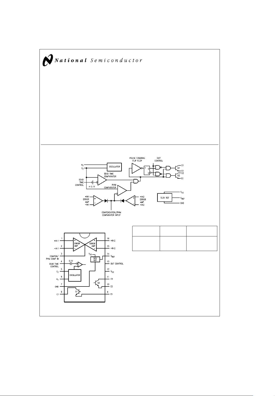
Block Diagram
TL/H/10056– 2
Connection Diagram
16-Lead DIP
TL/H/10056– 1
Top View
Ordering Information
Device Package Package
Code Code Description
LM494IN N16A Molded DIP
LM494CJ J16A Ceramic DIP
LM494CN N16A Molded DIP
C
1995 National Semiconductor Corporation RRD-B30M115/Printed in U. S. A.
Page 2
Absolute Maximum Ratings
If Military/Aerospace specified devices are required,
please contact the National Semiconductor Sales
Office/Distributors for availability and specifications.
Storage Temperature Range
Ceramic DIP
b
65§Ctoa175§C
Molded DIP
b
65§Ctoa150§C
Operating Temperature Range
Industrial (LM494I)
b
40§Ctoa85§C
Commercial (LM494C) 0
§
Ctoa70§C
Lead Temperature
Ceramic DIP (Soldering, 60 sec.) 300
§
C
Molded DIP (Soldering, 10 sec.) 265
§
C
Internal Power Dissipation (Notes 1, 2)
16L-Ceramic DIP 1.50W
16L-Molded DIP 1.04W
Supply Voltage 42V
Voltage from Any Lead to Ground
(except Lead 8 and Lead 11) V
CC
a
0.3V
Output Collector Voltage 42V
Peak Collector Current
(I
C1
and IC2) 250 mA
ESD Susceptibility (to be determined)
Recommended Operating
Conditions
Power Supply Voltage (VCC) 7.0V to 40V
Voltage on Any Lead
except Leads 8 and 11
(Referenced to Ground) (V
I
)
b
0.3V to V
CC
a
0.3V
Output Voltage Collector (V
C1,VC2
)
b
0.3V to 40V
Output Collector Current (IC1,IC2) 200 mA
Timing Capacitor (CT) 470 pF to 10 mF
Timing Resistor (RT) 1.8 kX to 500 kX
Oscillator Frequency (f
OSC
) 1.0 kHz to 300 kHz
LM494
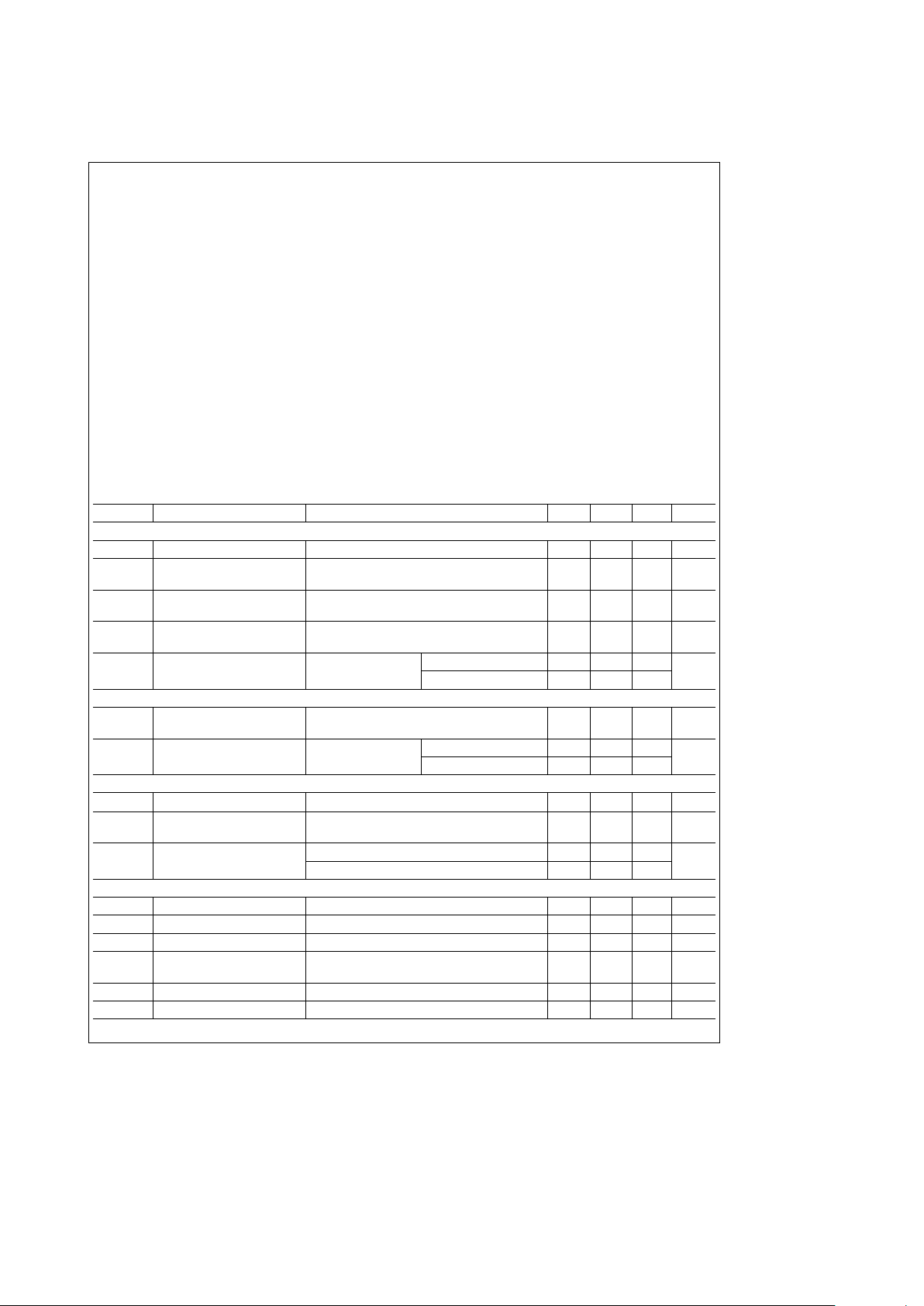
Electrical Characteristics
T
A
e
0§Ctoa70§C for the LM494C, T
A
eb
40§Ctoa85§C for the LM494I, V
CC
e
15V, f
OSC
e
10 kHz, unless otherwise specified
Symbol Parameter Conditions Min Typ Max Units
REFERENCE SECTION
V
REF
Reference Voltage (Note 3) I
REF
e
1.0 mA 4.75 5.0 5.25 V
Reg
LINE
Line Regulation of 7.0VsV
CC
s
40V
2.0 25 mV
Reference Voltage
TCV
REF
Temperature Coefficient of 0§CsT
A
s
70§C
0.01 0.03 %/
§
C
Reference Voltage
Reg
LOAD
Load Regulation of 1.0 mAsI
REF
s
10 mA
1.0 15 mV
Reference Voltage
I
OS
Output Short Circuit Current V
REF
e
0V 0§CsT
A
s
a
70§C103550
mA
b
40§CsT
A
s
a
85§C35
OSCILLATOR SECTION
f
OSC
Oscillator Frequency C
T
e
0.01 mF,
10 kHz
(Figure 10)
R
T
e
12 kX
Df
OSC
Oscillator Frequency Change C
T
e
0.01 mF, 0§CsT
A
s
a
70§C 2.0
%
R
T
e
12 kX
b
40§CsT
A
s
a
85§C 2.0
DEAD TIME CONTROL SECTION
I
IB (DT)
Input Bias Current V
CC
e
15V, 0VsV
4
s
5.25V
b
2.0b10 mA
DC
(Max)
Maximum Duty Cycle, V
CC
e
15V, Lead 4e0V,
45 %
Each Output Output Control
e
V
REF
V
TH(in)
Input Threshold Voltage Zero Duty Cycle 3.0 3.3
V
Maximum Duty Cycle 0
ERROR AMPLIFIER SECTIONS
V
IO
Input Offset Voltage V
3
e
2.5VV
3
e
2.5V 2.0 10 mV
I
IO
Input Offset Current V
3
e
2.5V 25 250 nA
I
IB
Input Bias Current V
3
e
2.5V 0.2 1.0 mA
V
ICR
Input Common Mode 7.0VsV
CC
s
40V
b
0.3 V
CC
V
Voltage Range
A
VS
Large Signal Voltage Gain 0.5VsV
3
s
3.5V 60 74 dB
BW Bandwidth 650 kHz
2
Page 3
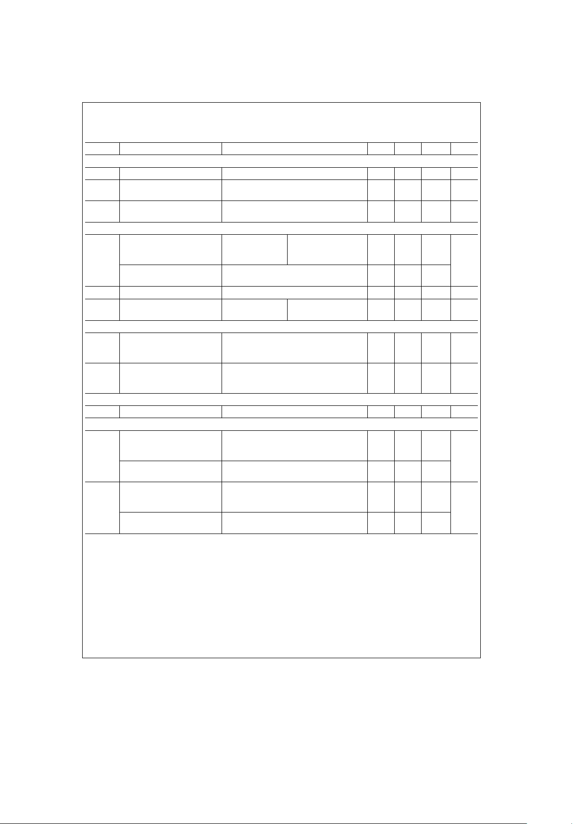
LM494
Electrical Characteristics
T
A
e
0§Ctoa70§C for the LM494C, T
A
eb
40§Ctoa85§C for the LM494I,
V
CC
e
15V, f
OSC
e
10 kHz, unless otherwise specified (Continued)
Symbol Parameter Conditions Min Typ Max Units
PWM COMPARATOR SECTION
(Figure 9)
V
THI
Inhibit Threshold Voltage Zero Duty Cycle 4.0 4.5 V
I
O
b
Output Sink Current 0.5VsV
3
s
3.5V
b
0.2b0.6 mA
(Note 4)
I
O
a
Output Source Current 0.5VsV
3
s
3.5V
2.0 mA
(Note 4)
OUTPUT SECTION
V
CE(sat)
Output Saturation V
E
e
0V, 0§CsT
A
s
a
70§C
Voltage Common Emitter I
C
e
200 mA
b
40§CsT
A
s
a
85§C 1.1 1.3
Configuration
(Figure 3)
V
Emitter Follower V
C
e
15V, I
E
e
200 mA
1.5 2.5
Configuration
(Figure 4)
I
C(off)
Collector Off-State Current V
CC
e
40V, V
CE
e
40V 2.0 100 mA
I
E(off)
Emitter Off-State Current V
CC
e
V
C
e
40V, 0§CsT
A
s
a
70§C,
b
100 mA
V
E
e
0
b
40§CsT
A
s
a
85§C
OUTPUT CONTROL
(Figure 6)
V
OCL
Output Control Voltage
Required for Single Ended or 0.4 V
Parallel Output Operation
V
OCH
Output Control Voltage
Required for Push-Pull 2.4 V
Operation
TOTAL DEVICE
I
CC
Standby Power Supply Current 6.0 10 mA
OUTPUT AC CHARACTERISTICS Use Recommended Operating Conditions with T
A
e
25§C
t
r
Rise Time of Output Voltage
Common Emitter Configuration 100 200
(Figure 3)
ns
Emitter Follower Configuration
100 200
(Figure 4)
t
f
Fall Time of Output Voltage
Common Emitter Configuration 25 100
(Figure 3)
ns
Emitter Follower Configuration
40 100
(Figure 4)
Note 1: T
J Max
e
150§C for the Molded DIP, and 175§C for the Ceramic DIP.
Note 2: Ratings apply to ambient temperature at 25
§
C. Above this temperature, derate the 16L-Ceramic DIP at 10 mW/§C, and the 16L-Molded DIP at 8.3 mW/§C.
Note 3: Selected devices with tightened tolerance reference voltage available.
Note 4: These limits apply when the voltage measured at Lead 3 is within the range specified.
3
Page 4

Functional Description
The basic oscillator (switching) frequency is controlled by an
external resistor (R
T
) and capacitor (CT). The relationship
between the values of R
T,CT
and frequency is shown in
Figure 10
.
The level of the sawtooth wave form is compared with an
error voltage by the pulse width modulated comparator. The
output of the PWM Comparator directs the pulse steering
flip-flop and the output control logic.
The error voltage is generated by the error amplifier. The
error amplifier boosts the voltage difference between the
output and the 5.0V internal reference. See
Figure 7
for
error amp sensing techniques. The second error amp is typically used to implement current-limiting.
The output control logic selects either push-pull or singleended operation of the output transistors (see
Figure 6
).
The dead time control prevents on-state overlap of the output transistors as can be seen in
Figure 5
. The dead time is
approximately 3.0% or 5.0% of the total period if the dead
time control is grounded. This dead time can be increased
by connecting the dead time control to a voltage up to 5.0V.
The frequency response of the error amps
(Figure 11)
can
be modified by using external resistors and capacitors.
These components are typically connected between the
compensation terminal and the inverting input of the error
amps.
The switching frequency of two or more LM494 circuits can
be synchronized. The timing capacitor, C
T
, is connected as
shown in
Figure 8
. Charging current is provided by the master circuit. Discharging is through all the circuits slaved to
the master. R
T
is required only for the master circuit.
Test Circuits
TL/H/10056– 3
FIGURE 1. Error Amplifier Test Circuit
TL/H/10056– 4
FIGURE 2. Current Limit Sense
Amplifier Test Circuit
TL/H/10056– 5
TL/H/10056– 6
FIGURE 3. Common Emitter Configuration
Test Circuit and Waveform
TL/H/10056– 7
TL/H/10056– 8
FIGURE 4. Emitter Follower Configuration
Test Circuit and Waveform
TL/H/10056– 9
FIGURE 5. Dead Time and Feedback
Control Test Circuit
4
Page 5

Typical Applications
TL/H/10056– 10
TL/H/10056– 11
FIGURE 6. Output Connections for Single Ended
and Push-Pull Configurations
TL/H/10056– 12 TL/H/10056– 13
FIGURE 7. Error Amplifier Sensing Techniques
TL/H/10056– 14
FIGURE 8. Slaving Two or More Control Circuits
5
Page 6

Typical Applications (Continued)
TL/H/10056– 15
FIGURE 9. Error Amplifier and Current Limit
Sense Amplifier Output Circuits
Typical Performance Characteristics
TL/H/10056– 16
FIGURE 10. Oscillator Frequency
vs Timing Resistance
TL/H/10056– 17
FIGURE 11. Amplifier Voltage Gain vs Frequency
6
Page 7

Voltage Waveforms
TL/H/10056– 18
Physical Dimensions inches (millimeters)
16-Lead Ceramic Dual-In-Line Package (J)
Order Number LM494CJ
NS Package Number J16A
7
Page 8

LM494 Pulse Width Modulated Control Circuit
Physical Dimensions inches (millimeters) (Continued)
16-Lead Molded Dual-In-Line Package (N)
Order Number LM494CN or LM494IN
NS Package Number N16A
LIFE SUPPORT POLICY
NATIONAL’S PRODUCTS ARE NOT AUTHORIZED FOR USE AS CRITICAL COMPONENTS IN LIFE SUPPORT
DEVICES OR SYSTEMS WITHOUT THE EXPRESS WRITTEN APPROVAL OF THE PRESIDENT OF NATIONAL
SEMICONDUCTOR CORPORATION. As used herein:
1. Life support devices or systems are devices or 2. A critical component is any component of a life
systems which, (a) are intended for surgical implant support device or system whose failure to perform can
into the body, or (b) support or sustain life, and whose be reasonably expected to cause the failure of the life
failure to perform, when properly used in accordance support device or system, or to affect its safety or
with instructions for use provided in the labeling, can effectiveness.
be reasonably expected to result in a significant injury
to the user.
National Semiconductor National Semiconductor National Semiconductor National Semiconductor
Corporation Europe Hong Kong Ltd. Japan Ltd.
1111 West Bardin Road Fax: (
a
49) 0-180-530 85 86 13th Floor, Straight Block, Tel: 81-043-299-2309
Arlington, TX 76017 Email: cnjwge@tevm2.nsc.com Ocean Centre, 5 Canton Rd. Fax: 81-043-299-2408
Tel: 1(800) 272-9959 Deutsch Tel: (
a
49) 0-180-530 85 85 Tsimshatsui, Kowloon
Fax: 1(800) 737-7018 English Tel: (
a
49) 0-180-532 78 32 Hong Kong
Fran3ais Tel: (
a
49) 0-180-532 93 58 Tel: (852) 2737-1600
Italiano Tel: (
a
49) 0-180-534 16 80 Fax: (852) 2736-9960
National does not assume any responsibility for use of any circuitry described, no circuit patent licenses are implied and National reserves the right at any time without notice to change said circuitry and specifications.
 Loading...