

Page 1
December 2006
LM49270
Filterless 2.2W Stereo Class D Audio Subsystem with OCL
Headphone Amplifier, 3D Enhancement, and Headphone
Sense
General Description
The LM49270 is a fully integrated audio subsystem designed
for stereo multimedia applications. The LM49270 combines a
2.2W stereo Class D amplifier with a 155mW stereo headphone amplifier, volume control, headphone sense, and
National’s unique 3D sound enhancement into a single device. The LM49270 uses flexible I2C control interface for
multiple application requirements.
The filterless stereo class D amplifiers delivers 2.2W/channel
into a 4Ω load with less than 10% THD+N with a 5V supply.
The headphone amplifier features National’s Output Capacitor-less (OCL) architecture that eliminates the output coupling
capacitors required by traditional headphone amplifiers.
The IC features a headphone sense input (HPS) that automatically detects the presence of a headphone and configures the device accordingly. The LM49270 can automatically
switch from OCL headphone output to a line driver output. If
the VOC pin is pulled to GND, the VOC amplifier is disabled
and the VOC pin is internally set to GND. This feature allows
the LM49270 to be used as a line driver in OCL mode without
a GND conflict on the headphone jack sleeve. Additionally,
the headphone amplifier can be configured as capacitively
coupled (CC).
The LM49270 features a 32 step volume control for the headphone and stereo outputs. The device mode select and volume are controlled through an I2C compatible interface.
Output short circuit and thermal shutdown protection prevent
the device from being damaged during fault conditions. Superior click and pop suppression eliminates audible transients
on power-up/down and during shutdown. The LM49270 is
available in a space saving 28-pin, 5x5mm LLP package.
Key Specifications
■ Stereo Class D Amplifier Efficiency:
V
DD
= 3.3V, 450mW/Ch into 8Ω
84%
V
DD
= 5V, 1W/Ch into 8Ω
84%
■ Quiescent Power Supply Current, V
DD
= 3.3V
Speaker Mode 5.5mA
Headphone Mode (OCL) 4mA
■ Power Output/Channel, V
DD
= 5V
Class D Speaker amplifier:
RL = 4Ω, THD+N = ≤ 10%
2.2W
RL = 8Ω, THD+N = ≤ 1%
1.06W
Headphone amplifier:
RL = 16Ω, THD+N = ≤ 1%
155mW
RL = 32Ω, THD+N = ≤ 1%
90mW
■ Shutdown current
0.02μA
Features
■
Stereo filterless Class D amplifier
■
Selectable OCL/CC headphone amplifier
■
Headphone sense ability
■
National’s 3D Enhancement
■
RF suppression
■
I2C control interface
■
32-step digital volume control
■
6 Operating Modes
■
Output short circuit protection and thermal shutdown
protection
■
Minimum external components
■
Click and Pop suppression
■
Micro-power shutdown
■
Independent speaker and headphone volume controls
■
Available in space-saving 28 pin LLP package
Applications
■
Portable DVD players
■
Smart phones
■
PDAs
■
Laptops
Boomer® is a registered trademark of National Semiconductor Corporation.
© 2007 National Semiconductor Corporation 202129 www.national.com
LM49270 Filterless 2.2W Stereo Class D Audio Subsystem with OCL Headphone Amplifier, 3D
Enhancement, and Headphone Sense
Page 2
Typical Application
20212994
FIGURE 1. Typical Audio Amplifier Application Circuit
www.national.com 2
LM49270
Page 3
Connection Diagrams
SQ Package
5mm x 5mm x 0.8mm
20212990
Top View
Order Number LM49270SQ
See NS Package Number NSQAQ028
SQ Markings
20212901
Top View
NS = National Logo
U = Fab Code
Z = Assembly Plant
XY = 2 Digit date code
TT = Die Traceability
49270SQ = LM49270SQ
3 www.national.com
LM49270
Page 4
TABLE 1. Pin Descriptions
PIN NAME DESCRIPTION
1 RHP Right channel headphone output
2 VOC VDD/2 buffer output
3 LHP Left channel headphone output
4 HPV
DD
Headphone supply input
5 R3DIN Right channel 3D input
6 L3DIN Left channel 3D input
7 BYPASS Bias bypass
8 LIN Left channel input
9 RIN Right channel input
10 GND Analog ground
11 NC No connect
12 LSV
DD
Speaker supply voltage input
13 RLS+ Right channel non-inverting speaker output
14 RLS- Right channel inverting speaker output
15 NC No connect
16 NC No connect
17 I2CV
DD
I2C supply voltage input
18 LSGND Speaker ground
19 V
DD
Power supply
20 ADR Address
21 NC No connect
22 LLS- Left channel inverting speaker output
23 LLS+ Left channel non-inverting speaker output
24 LSV
DD
Speaker supply voltage input
25 SDA Serial data input
26 SCL Serial clock input
27 HPS Headphone sense input
28 GND Headphone ground
www.national.com 4
LM49270
Page 5
Absolute Maximum Ratings (Notes 1, 2)
If Military/Aerospace specified devices are required,
please contact the National Semiconductor Sales Office/
Distributors for availability and specifications.
Supply Voltage (Note 1) 6.0V
Storage Temperature −65°C to +150°C
Input Voltage –0.3V to VDD +0.3V
Power Dissipation (Note 3) Internally Limited
ESD Susceptibility(Note 4) 2000V
ESD Susceptibility (Note 5) 200V
Junction Temperature (T
JMAX
)
150°C
Thermal Resistance
θ
JA
35.1°C/W
Operating Ratings (Notes 1, 2)
Temperature Range
T
MIN
≤ TA ≤ T
MAX
−40°C ≤ TA ≤ 85°C
Supply Voltage
(VDD, LSVDD, HPVDD)
2.4V ≤ VDD ≤ 5.5V
I2C Voltage (I2CVDD)
2.4V ≤ I2CVDD ≤ 5.5V
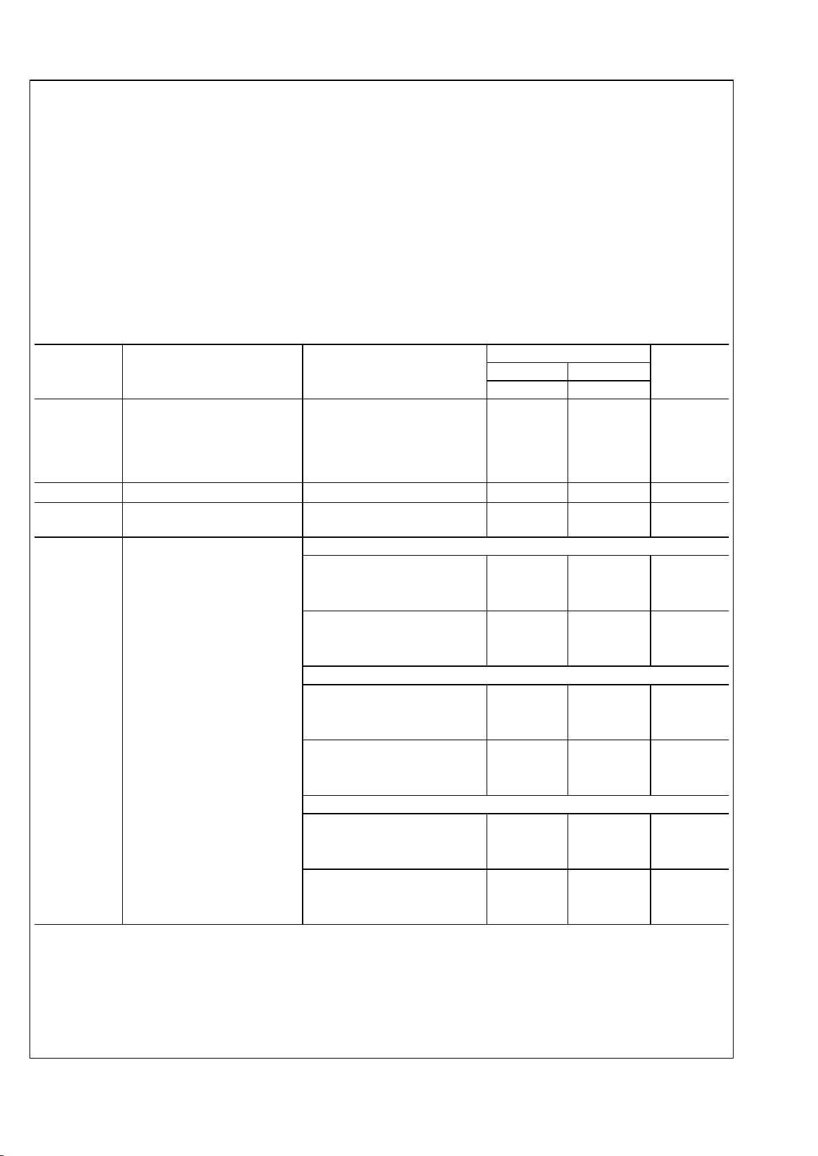
Electrical Characteristics VDD = 3.3V (Notes 1, 2) The following specifications apply for Headphone:
AV = 0dB, R
L(HP)
= 32Ω; for Loudspeakers: AV = 6dB, R
L(SP)
= 15μH + 8Ω + 15μH , f = 1kHz, unless otherwise specified. Limits
apply for TA = 25°C.
Symbol Parameter Conditions
LM49270
Units
(Limits)
Typical Limit
(Note 6) (Notes 7, 8)
I
DD
Supply Current
VIN = 0, RL = No Load,
Both channels active
Speaker ON, HP OFF
Speaker OFF, CC HP ON
Speaker OFF, OCL HP ON
5.5
3
4
7.6
4.7
5.75
mA (max)
mA (max)
mA (max)
I
SD
Shutdown Supply Current 0.02 2
μA (max)
V
OS
Output Offset Voltage
Headphone
Speaker
10
10
25
60
mV (max)
mV (max)
P
OUT
Output Power
Speaker Mode, f = 1kHz
THD+N = 1%
RL = 4Ω
RL = 8Ω
700
450 400
mW
mW (min)
THD+N = 10%
RL = 4Ω
RL = 8Ω
870
560
mW
mW
CC Headphone Mode, f = 1kHz
THD+N = 1%
RL = 16Ω
RL = 32Ω
60
36 30
mW
mW (min)
THD+N = 10%
RL = 16Ω
RL = 32Ω
74
55
mW
mW
OCL Headphone Mode, f = 1kHz
THD+N = 1%
RL = 16Ω
RL = 32Ω
60
36 30
mW
mW (min)
THD+N = 10%
RL = 16Ω
RL = 32Ω
73
55
mW
mW
5 www.national.com
LM49270
Page 6
Symbol Parameter Conditions
LM49270
Units
(Limits)
Typical Limit
(Note 6) (Notes 7, 8)
THD+N Total Harmonic Distortion + Noise
Speaker Mode, f = 1kHz
P
OUT
= 100mW, RL = 8Ω
0.02
%
CC Headphone Mode,
f = 1kHz
P
OUT
= 12mW, RL = 32Ω
0.015
%
OCL Headphone Mode,
f = 1kHz
P
OUT
= 12mW, RL = 32Ω
0.02
%
e
N
Noise
Speaker Mode,
A-Wtg, Input Referred
47
μV
CC Headphone Mode,
A-Wtg, Input Referred
10
μV
OCL Headphone Mode, A-Wtg,
Input Referred
11
μV
η
Efficiency
Speaker Mode
RL = 8Ω
84 %
Xtalk Crosstalk
Speaker Mode,
f = 1kHz, VIN = 1Vp-p
71 dB
CC Headphone Mode,
f = 1kHz, VIN = 1Vp-p
70 dB
OCL Headphone Mode,
f = 1kHz, VIN = 1Vp-p
55 dB
T
ON
Turn-on Time
30 ms
T
OFF
Turn-off Time
64 ms
Z
IN
Input Impedance
Maximum Gain
23.5
kΩ
Minimum Gain
210
kΩ
A
V
Gain
Maximum Gain, Speaker Mode 30 dB
Minimum Gain, Speaker Mode –47 dB
Maximum Gain, Headphone Mode 18 dB
Minimum Gain, Headphone Mode –59 dB
PSRR Power Supply Rejection Ratio
Speaker Mode,
V
RIPPLE
= 200mVp-p Sine
f = 217Hz
f = 1kHz
68
68
dB
dB
Headphone Mode,
V
RIPPLE
= 200mVp-p Sine, CC
Mode
f = 217Hz
f = 1kHz
73
73
dB
dB
Headphone Mode,
V
RIPPLE
= 200mVp-p Sine, OCL
Mode
f = 217Hz
f = 1kHz
75
79
dB
dB
HPS
(Th)
Headphone Sense Threshold
Detect Headphone 2.9 V (min)
Detect no Headphone 1.8 V (max)
www.national.com 6
LM49270
Page 7
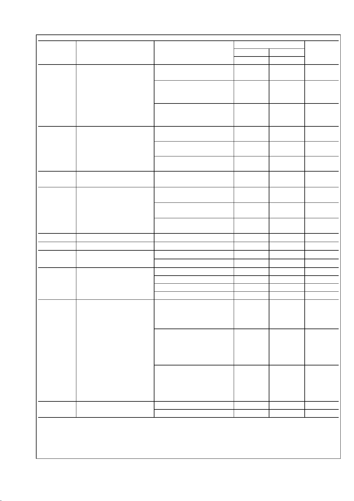
Electrical Characteristics VDD = 5.0V (Notes 2, 1) The following specifications apply for Headphone”
AV = 0dB, R
L(HP)
= 32Ω,: for Loudspeakers: AV = 6dB, R
L(SP
) = 15μH + 8Ω + 15μH, f = 1kHz unless otherwise specified. Limits
apply for TA = 25°C.
Symbol Parameter Conditions
LM49270
Units
(Limits)
Typical Limit
(Note 6) (Notes 7, 8)
I
DD
Supply Current
VIN = 0, RL = No Load,
Both channels active
Speaker ON, HP OFF
Speaker OFF, CC HP ON
Speaker OFF, OCL HP ON
8.5
3.6
4.7
12.4
5.5
6.5
mA (max)
mA (max)
mA (max)
I
SD
Shutdown Supply Current 0.15 2
μA (max)
V
OS
Output Offset Voltage
Headphone
Speaker
10
10
25
60
mV (max)
mV (max)
P
OUT
Output Power
Speaker Mode, f = 1kHz,
THD+N = 1%
RL = 4Ω
RL = 8Ω
1.75
1.06
W
W
THD+N = 10 %
RL = 4Ω
RL = 8Ω
2.2
1.35
W
W
CC Headphone Mode, f = 1kHz,
THD+N = 1%
RL = 16Ω
RL = 32Ω
155
90
mW
mW
THD+N = 10%
RL = 16Ω
RL = 32Ω
177
140
mW
mW
OCL Headphone Mode, f = 1kHz,
THD+N = 1%
RL = 16Ω
RL = 32Ω
155
90
mW
mW
THD+N = 10%
RL = 16Ω
RL = 32Ω
175
140
mW
mW
THD+N
Total Harmonic Distortion +
Noise
Speaker Mode, f = 1kHz
P
OUT
= 100mW, RL = 8Ω
0.03
%
CC Headphone Mode,
f = 1kHz
P
OUT
= 12mW, RL = 32Ω
0.02
%
OCL Headphone Mode,
f = 1kHz
P
OUT
= 12mW, RL = 32Ω
0.03
%
e
N
Noise
Speaker Mode,
A-Wtg, Input Referred
47
μV
CC Headphone Mode,
A-Wtg, Input Referred
10
μV
OCL Headphone Mode,
A-Wtg, Input Referred
11
μV
η
Efficiency
Speaker Mode
RL = 8Ω
84 %
7 www.national.com
LM49270
Page 8
Symbol Parameter Conditions
LM49270
Units
(Limits)
Typical Limit
(Note 6) (Notes 7, 8)
Xtalk Crosstalk
Speaker Mode,
f = 1kHz, VIN = 1Vp-p
–85 dB
CC Headphone Mode,
f = 1kHz, VIN = 1Vp-p
–70 dB
OCL Headphone Mode,
f = 1kHz, VIN = 1Vp-p
–58 dB
T
ON
Turn-on Time
43 ms
T
OFF
Turn-off Time
100 ms
Z
IN
Input Impedance
Maximum Gain
23.5
kΩ
Minimum Gain
210
kΩ
A
V
Gain
Maximum Gain, Speaker Mode 30 dB
Minimum Gain, Speaker Mode –47 dB
Maximum Gain, Headphone Mode 18 dB
Minimum Gain, Headphone Mode –59 dB
PSRR Power Supply Rejection Ratio
Speaker Mode,
V
RIPPLE
= 200mVp-p Sine
f = 217Hz
f = 1kHz
61
61
dB
dB
Headphone Mode,
V
RIPPLE
= 200mVp-p Sine, CC
Mode
f = 217Hz
f = 1kHz
75
74
dB
min
Headphone Mode,
V
RIPPLE
= 200mVp-p Sine, OCL
Mode
f = 217Hz
f = 1kHz
78
75
dB
dB
HPS
(Th)
Headphone Sense Threshold
Detect Headphone 4.4 V (min)
Detect no Headphone 3 V (max)
Note 1: All voltages are measured with respect to the ground pin, unless otherwise specified.
Note 2: Absolute Maximum Ratings indicate limits beyond which damage to the device may occur. Operating Ratings indicate conditions for which the device is
functional, but do not guarantee specific performance limits. Electrical Characteristics state DC and AC electrical specifications under particular test conditions
which guarantee specific performance limits. This assumes that the device is within the Operating Ratings. Specifications are not guaranteed for parameters
where no limit is given, however, the typical value is a good indication of device performance.
Note 3: The maximum power dissipation must be derated at elevated temperatures and is dictated by T
JMAX
, θJA, and the ambient temperature, TA. The maximum
allowable power dissipation is P
DMAX
= (T
JMAX
– TA)/ θJA or the number given in Absolute Maximum Ratings, whichever is lower. For the LM49270 see power
derating currents for more information.
Note 4: Human body model, 100pF discharged through a 1.5kΩ resistor.
Note 5: Machine Model, 220pF–240pF discharged through all pins.
Note 6: Typicals are measured at 25°C and represent the parametric norm.
Note 7: Limits are guaranteed to National's AOQL (Average Outgoing Quality Level).
Note 8: Datasheet min/max specification limits are guaranteed by design, test, or statistical analysis.
www.national.com 8
LM49270
Page 9

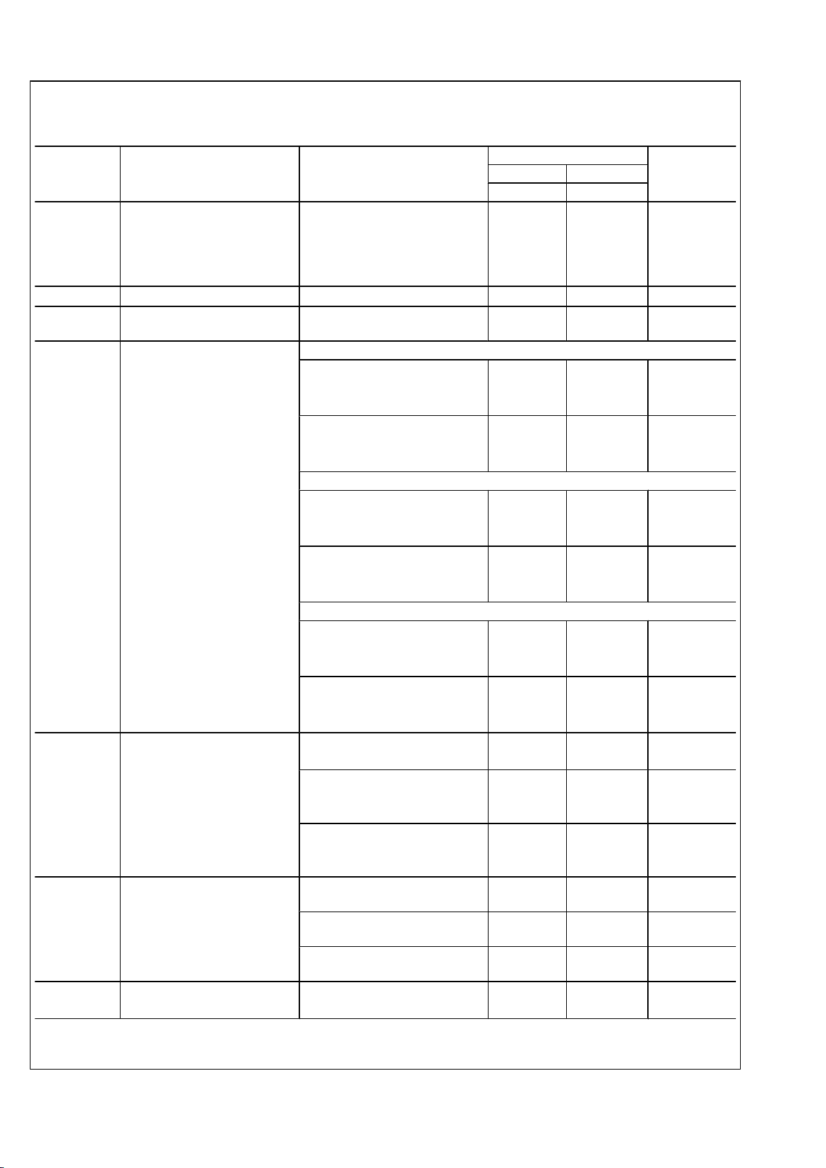
Typical Performance Characteristics
THD+N vs Output Power
Speaker Mode
AV = 6dB, RL = 4Ω, f = 1kHz
20212902
THD+N vs Output Power
Speaker Mode
AV = 6dB, RL = 8Ω, f = 1kHz
20212903
THD+N vs Output Power
OCL Headphone Mode
AV = 0dB, RL = 16Ω, f = 1kHz
20212908
THD+N vs Output Power
OCL Headphone Mode
AV = 0dB, RL = 32Ω, f = 1kHz
20212909
THD+N vs Output Power
CC Headphone Mode
AV = 0dB, RL = 16Ω, f = 1kHz
20212914
THD+N vs Output Power
CC Headphone Mode
AV = 0dB, RL = 32Ω, f = 1kHz
20212915
9 www.national.com
LM49270
Page 10

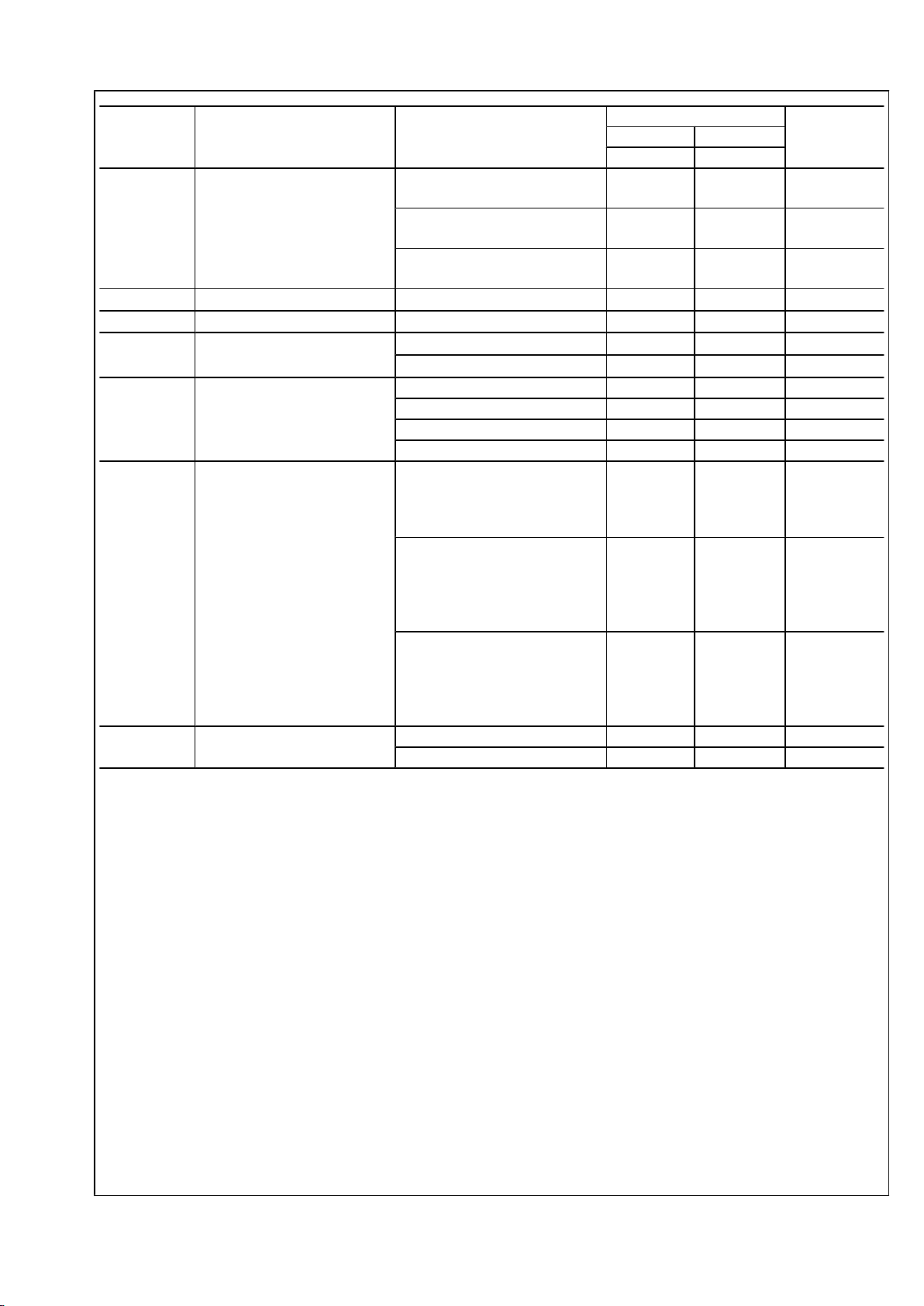
THD+N vs Frequency
Speaker Mode
VDD = 3.3V, P
OUT
= 300mW, RL = 4Ω
20212904
THD+N vs Frequency
Speaker Mode
VDD = 5V, P
OUT
= 500mW, RL = 4Ω
20212905
THD+N vs Frequency
Speaker Mode
VDD = 3.3V, P
OUT
= 200mW, RL = 8Ω
20212906
THD+N vs Frequency
Speaker Mode
VDD = 5V, P
OUT
= 350mW, RL = 8Ω
20212907
THD+N vs Frequency
OCL Headphone Mode
VDD = 3.3V, P
OUT
= 45mW, RL = 16Ω
20212910
THD+N vs Frequency
OCL Headphone Mode
VDD = 5V, P
OUT
= 100mW, RL = 16Ω
20212911
www.national.com 10
LM49270
Page 11

THD+N vs Frequency
OCL Headphone Mode
VDD = 3.3V, P
OUT
= 25mW, RL = 32Ω
20212912
THD+N vs Frequency
OCL Headphone Mode
VDD = 5V, P
OUT
= 70mW, RL = 32Ω
20212913
THD+N vs Frequency
CC Headphone Mode
VDD = 3.3V, P
OUT
= 45mW, RL = 16Ω
20212916
THD+N vs Frequency
CC Headphone Mode
VDD = 5V, P
OUT
= 100mW, RL = 16Ω
20212917
THD+N vs Frequency
CC Headphone Mode
VDD = 3.3V, P
OUT
= 25mW, RL = 32Ω
20212918
THD+N vs Frequency
CC Headphone Mode
VDD = 5V, P
OUT
= 70mW, RL = 32Ω
20212919
11 www.national.com
LM49270
Page 12

PSRR vs Frequency
Speaker Mode
VDD = 3.3V, V
RIPPLE
= 200mV
P-P
, RL = 8Ω
202129a2
PSRR vs Frequency
OCL Headphone Mode
VDD = 3.3V, V
RIPPLE
= 200mV
P-P
, RL = 32Ω
202129a3
PSRR vs Frequency
CC Headphone Mode
VDD = 3.3V, V
RIPPLE
= 200mV
P-P
, RL = 32Ω
202129a4
Efficiency vs Output Power
Speaker Mode
RL = 4Ω, f = 1kHz
20212967
Efficiency vs Output Power
Speaker Mode
RL = 8Ω, f = 1kHz
20212968
Power Dissipation vs Output Power
Speaker Mode
RL = 4Ω, f = 1kHz
20212969
www.national.com 12
LM49270
Page 13

Power Dissipation vs Output Power
Speaker Mode
RL = 8Ω, f = 1kHz
20212970
Power Dissipation vs Output Power
OCL Headphone Mode
RL = 16Ω, f = 1kHz
20212998
Power Dissipation vs Output Power
OCL Headphone Mode
RL = 32Ω, f = 1kHz
20212977
Power Dissipation vs Output Power
CC Headphone Mode
RL = 16Ω, f = 1kHz
20212982
Power Dissipation vs Output Power
CC Headphone Mode
RL = 32Ω, f = 1kHz
20212983
Output Power vs Supply Voltage
Speaker Mode
RL = 4Ω, f = 1kHz
20212971
13 www.national.com
LM49270
Page 14

Output Power vs Supply Voltage
Speaker Mode
RL = 8Ω, f = 1kHz
20212972
Output Power vs Supply Voltage
OCL Headphone Mode
RL = 16Ω, f = 1kHz
20212995
Output Power vs Supply Voltage
OCL Headphone Mode
RL = 32Ω, f = 1kHz
20212996
Output Power vs Supply Voltage
CC Headphone Mode
RL = 16Ω, f = 1kHz
20212997
Output Power vs Supply Voltage
CC Headphone Mode
RL = 32Ω, f = 1kHz
20212985
Crosstalk vs Frequency
Speaker Mode
VDD = 3.3V, V
RIPPLE
= 1V
P-P
, RL = 8Ω
202129a0
www.national.com 14
LM49270
Page 15

Crosstalk vs Frequency
OCL Headphone Mode
VDD = 3.3V, V
RIPPLE
= 1V
P-P
, RL = 32Ω
20212989
Crosstalk vs Frequency
CC Headphone Mode
VDD = 3.3V, V
RIPPLE
= 1V
P-P
, RL = 32Ω
202129a1
Supply Current vs Supply Voltage
Speaker Mode, No Load
20212975
Supply Current vs Supply Voltage
OCL Headphone Mode, No Load
20212981
Supply Current vs Supply Voltage
CC Headphone Mode, No Load
20212988
Turn-On
Speaker Mode
20212927
15 www.national.com
LM49270
Page 16

Turn-Off
Speaker Mode
20212928
Turn-On
OCL Headphone Mode
20212929
Turn-Off
OCL Headphone Mode
20212930
Turn-On
CC Headphone Mode
20212931
Turn-Off
CC Headphone Mode
20212932
www.national.com 16
LM49270
Page 17

Application Information
I2C COMPATIBLE INTERFACE
The LM49270 is controlled through an I2C compatible serial
interface that consists of a serial data line (SDA) and a serial
clock (SCL). The clock line is uni-directional. The data line is
bi-directional (open-collector), although the LM49270 does
not write to the I2C bus. The LM49270 and the master can
communicate at clock rates up to 400kHz. Figure 3 shows the
I2C interface timing diagram. The LM49270 is a transmit/receive slave-only device, reliant upon the master to generate
a clock signal.
The master device communicates to the LM49270 by transmitting the proper device address followed by a command
word. Each transmission sequence is framed by a START
condition and a STOP condition. Each word (register address
+ register content) transmitted over the bus is 8 bits long and
is always followed by an acknowledge pulse.
To avoid an address conflict with another device on the I2C
bus, the LM49270 address is determined by the ADR pin, the
state of ADR determines address bit A1 (Table 2). When ADR
= 0, the address is 1111 1000. When ADR = 1 the device
address is 1111 1010.
TABLE 2. Device Address
ADR A7 A6 A5 A4 A3 A2 A1 A0
X 1 1 1 1 1 0 X 0
0 1 1 1 1 1 0 0 0
1 1 1 1 1 1 0 1 0
TABLE 3. I2C Control Registers
REG Register Name D7 D6 D5 D4 D3 D2 D1 D0
0 Shutdown Control 0 0
— —
HP3DSEL LS3DSEL OCL/CC PWR_ON
1 Headphone Gain Control 0 1
—
HP4 HP3 HP2 HP1 HP0
2 Speaker Gain Control 1 0
—
LS4 LS3 LS2 LS1 LS0
Note: OCL/CC = 1 selects OCL mode; OCL/CC = 0 selects
cap coupled mode
PWR_ON = 0 puts part in shutdown
BUS FORMAT
The I2C bus format is shown in Figure 2. The “start” signal is
generated by lowering the data signal while the clock is high.
The start signal alerts all devices on the bus that a device
address is being written to the bus.
The 8-bit device address is written to the bus next, most significant bit first. The data is latched in on the rising edge of the
clock. Each address bit must be stable while the clock is high.
After the last address bit is sent, the master device releases
the data line, during which time, an acknowledge clock pulse
is generated. If the LM49270 receives the address correctly,
then the LM49270 pulls the data line low, generating an acknowledge bit (ACK).
Once the master device has registered the ACK bit, the 8-bit
register address/data word is sent. Each data bit should be
stable while the clock level is high. After the 8–bit word is sent,
the LM49270 sends another ACK bit. Following the acknowledgement of the data word, the master device issues a “stop”
bit, allowing SDA to go high while the clock signal is high.
20212991
FIGURE 2. I2C Bus Format
17 www.national.com
LM49270
Page 18

20212992
FIGURE 3. I2C Timing Diagram
GENERAL AMPLIFIER FUNCTION
Class D Amplifier
The LM49270 features a high-efficiency, filterless, Class D
stereo amplifier. The LM49270 Class D amplifiers feature a
filterless modulation scheme known as Class BD. The differential outputs of each channel switch at 300kHz from VDD to
GND. When there is no input signal applied, the two outputs
(LLS+ and LLS-) switch in phase with a 50% duty cycle. Because the outputs of the LM49270 are differential, there is in
no net voltage across the speaker, thus no load current during
the idle state conserving power.
When an input signal is applied, the duty cycle (pulse width)
of each output changes. For increasing output voltages, the
duty cycle of LLS+ increases, while the duty cycle of LLSdecreases. For decreasing output voltages, the converse
occurs. The duty cycle of LLS- increases while the duty cycle
of LLS+ decreases. The difference between the two pulse
widths yields the differential output voltage.
Headphone Amplifier
The LM49270 headphone amplifier features two different operating modes, output capacitor-less (OCL) and capacitor
coupled (CC). The OCL architecture eliminates the bulky, expensive output coupling capacitors required by traditional
headphone amplifiers. The LM49270 headphone section uses three amplifiers. Two amplifiers drive the headphones
while the third (VOC) is set to the internally generated bias
voltage (typically VDD/2). The third amplifier is connected to
the return terminal (sleeve) of the headphone jack. In this
configuration, the signal side of the headphones are biased
to VDD/2, the return is biased to VDD/2, thus there is no net DC
voltage across the headphone eliminating the need for an
output coupling capacitor. Removing the output coupling capacitors from the headphone signal path reduces component
count, reducing system cost and board space consumption,
as well as improving low frequency performance and sound
quality. The voltage on the return sleeve is not an issue when
driving headphones. However, if the headphone output is
used as a line out, the VDD/2 can conflict with the GND potential that a line-in would expect on the return sleeve. When
the return of the headphone jack is connected to GND, the
LM49270 detects an output short circuit condition and the
VOC amplifier is disabled preventing damage to the LM49270
and allowing the headphone return to be biased at GND.
Capacitor Coupled Headphone Mode
In capacitor coupled (CC) mode, the VOC pin is disabled, and
the headphone outputs are coupled to the jack through series
capacitors, allowing the headphone return to be connected to
GND (Figure 4). In CC mode, the LM49270 requires output
coupling capacitors to block the DC component of the amplifier output, preventing DC current from flowing to the load.
The output capacitor and speaker impedance form a high
pass filter with a -3dB roll-off determined by:
f
-3dB
= 1 / 2πRLC
OUT
Where RL is the headphone impedance, and C
OUT
is the out-
put coupling capacitor. Choose C
OUT
such that f
-3dB
is well
below the lowest frequency of interest. Setting f
-3dB
too high
results in poor low frequency performance. Select capacitor
dielectric types with low ESR to minimize signal loss due to
capacitor series resistance and maximize power transfer to
the load.
20212993
FIGURE 4. Capacitor Coupled Headphone Mode
Headphone Sense
The LM49270 features a headphone sense input (HPS) that
monitors the headphone jack and configures the device depending on the presence of a headphone. When the HPS pin
is low, indicating that a headphone is not present, the
LM49270 speaker amplifiers are active and the headphone
www.national.com 18
LM49270
Page 19

amplifiers are disabled. When the HPS pin is high, indicating
that a headphone is present, the headphone amplifiers are
active while the speaker amplifiers are disabled.
POWER DISSIPATION AND EFFICIENCY
The major benefit of Class D amplifier is increased efficiency
versus Class AB. The efficiency of the LM49270 speaker amplifiers is attributed to the output transistors’ region of operation. The Class D output stage acts as current steering
switches, consuming negligible amounts of power compared
to their Class AB counterparts. Most of the power loss associated with the output stage is due to the IR loss of the
MOSFET on-resistance (R
DS(ON)
) , along with the switching
losses due to gate charge.
The maximum power dissipation per headphone channel in
Capacitor Coupled mode is given by:
P
DMAX(CC)
= V
DD
2
/2π2R
L
In OCL mode, the maximum power dissipation increases due
to the use of a third amplifier as a buffer. The power dissipation is given by:
P
DMAX(OCL)
= V
DD
2/π2
R
L
SHUTDOWN FUNCTION
The LM49270 features a shutdown mode configured through
the I2C interface. Bit D0 (PWR_ON) in the Shutdown Control
register shuts down/turns on the entire device. Set PWR_ON
= 1 to enable the LM49270, set PWR_ON = 0 to disable the
device.
AUDIO AMPLIFIER GAIN SETTING
Each channel of the LM49270 features a 32 step volume control. The loudspeaker volume has a range of -47dB to 30dB
and the headphone has a range of -59dB to 18dB (see Table
4).
TABLE 4. Volume Control
Volume Step LS4/HP4 LS3/HP3 LS2/HP2 LS1/HP1 LS0/HP0 LS
Gain (dB)
HP
Gain (dB)
1 0 0 0 0 0 –47 –59
2 0 0 0 0 1 –36 –48
3 0 0 0 1 0 –28.5 –46.5
4 0 0 0 1 1 –22.5 –34.5
5 0 0 1 0 0 –18 –30
6 0 0 1 0 1 –15 –27
7 0 0 1 1 0 –12 –24
8 0 0 1 1 1 –9 –21
9 0 1 0 0 0 –6 –18
10 0 1 0 0 1 –3 –15
11 0 1 0 1 0 –1.5 –13.5
12 0 1 0 1 1 0 –12
13 0 1 1 0 0 1.5 –10.5
14 0 1 1 0 1 3 –9
15 0 1 1 1 0 4.5 –7.5
16 0 1 1 1 1 6 –6
17 1 0 0 0 0 7.5 –4.5
18 1 0 0 0 1 9 –3
19 1 0 0 1 0 10.5 –1.5
20 1 0 0 1 1 12 0
21 1 0 1 0 0 13.5 1.5
22 1 0 1 0 1 15 3
23 1 0 1 1 0 16.5 4.5
24 1 0 1 1 1 18 6
25 1 1 0 0 0 19.5 7.5
26 1 1 0 0 1 21 9
27 1 1 0 1 0 22.5 10.5
28 1 1 0 1 1 24 12
29 1 1 1 0 0 25.5 13.5
30 1 1 1 0 1 27 15
31 1 1 1 1 0 28.5 16.5
32 1 1 1 1 1 30 18
19 www.national.com
LM49270
Page 20

NATIONAL 3D ENHANCEMENT
The LM49720 features National’s 3D sound enhancement.
3D sound improves the apparent stereo channel separation
whenever the left and right speakers are located close to each
other, widening the perceived sound stage in devices with a
small form factor that prohibits proper speaker placement.
An external RC network , shown in Figure 1, enables the 3D
effect. R3D sets the level of the 3D effect; decreasing the value of R3D will increase the 3D effect. The 3D network acts
like a high pass filter C3D sets the frequency response; increasing the value of C3D will decrease the low cutoff frequency at which the 3D effect starts to occur, as shown by
this equation:
f
3D(-3dB)
= 1/2π(R3D)(C3D) (1)
Enabling the 3D effect increases the gain by a multiplication
factor of (1 + 20kΩ/R3D). Setting R3D to 20kΩ results in a
6dB increase (doubling) of the gain, increasing the 3D effect.
The level of 3D effect is also dependent on other factors such
as speaker placement and the distance from the speakers to
the listener. The values of R3D and C3D should be chosen
for each application individually, taking into account the physical factors noted before.
POWER SUPPLIES
The LM49270 uses different supplies for each portion of the
device, allowing for the optimum combination of headroom,
power dissipation and noise immunity. The speaker amplifier
gain stage is powered from VDD, while the output stage is
powered from LSVDD. The headphone amplifiers, input amplifiers and volume control stages are powered from HPVDD.
The separate power supplies allow the speakers to operate
from a higher voltage for maximum headroom, while the
headphones operate from a lower voltage, improving power
dissipation. HPVDD may be driven by a linear regulator to further improve performance in noisy environments. The I2C
portion if powered from I2CVDD, allowing the I2C portion of the
LM49270 to interface with lower voltage digital controllers.
PROPER SELECTION OF EXTERNAL COMPONENTS
Audio Amplifier Power Supply Bypassing/Filtering
Proper power supply bypassing is critical for low noise performance and high PSRR. Place the supply bypass capacitor
as close to the device as possible. Typical applications employ a voltage regulator with 10µF and 0.1µF bypass capacitors that increase supply stability. These capacitors do not
eliminate the need for bypassing of the LM49270 supply pins.
A 1µF capacitor is recommended.
Bypass Capacitor Selection
The LM49270 generates a VDD/2 common-mode bias voltage
internally. The BYPASS capacitor, CB, improves PSRR and
THD+N by reducing noise at the BYPASS node. Use a 1μF
capacitor, placed as close to the device as possible for CB.
Audio Amplifier Input Capacitor Selection
Input capacitors, CIN, in conjunction with the input impedance
of the LM49270 forms a high pass filter that removes the DC
bias from an incoming signal. The AC-coupling capacitor allows the amplifier to bias the signal to an optimal DC level.
Assuming zero source impedance, the -3dB point of the high
pass filter is given by:
f
(–3dB)
= 1/2πRINC
IN
(2)
Choose CIN such that f
-3dB
is well below that lowest frequency
of interest. Setting f
-3dB
too high affects the low-frequency responses of the amplifier. Use capacitors with low voltage
coefficient dielectrics, such as tantalum or aluminum electrolytic. Capacitors with high-voltage coefficients, such as
ceramics, may result in increased distortion at low frequencies. Other factors to consider when designing the input filter
include the constraints of the overall system. Although high
fidelity audio requires a flat frequency response between
20Hz and 20kHz, portable devices such as cell phones may
only concentrate on the frequency range of the frequency
range of the spoken human voice (typically 300Hz to 4kHz).
In addition, the physical size of the speakers used in such
portable devices limits the low frequency response; in this
case, frequencies below 150Hz may be filtered out.
www.national.com 20
LM49270
Page 21

Revision Table
Rev Date Description
1.0 12/19/06 Initial release.
21 www.national.com
LM49270
Page 22

Physical Dimensions inches (millimeters) unless otherwise noted
28 Lead LLP
Order Number LM49270SQ
NS Package Number NSQAQ028
www.national.com 22
LM49270
Page 23

Notes
23 www.national.com
LM49270
Page 24

Notes
LM49270 Filterless 2.2W Stereo Class D Audio Subsystem with OCL Headphone Amplifier, 3D
Enhancement, and Headphone Sense
THE CONTENTS OF THIS DOCUMENT ARE PROVIDED IN CONNECTION WITH NATIONAL SEMICONDUCTOR CORPORATION
(“NATIONAL”) PRODUCTS. NATIONAL MAKES NO REPRESENTATIONS OR WARRANTIES WITH RESPECT TO THE ACCURACY
OR COMPLETENESS OF THE CONTENTS OF THIS PUBLICATION AND RESERVES THE RIGHT TO MAKE CHANGES TO
SPECIFICATIONS AND PRODUCT DESCRIPTIONS AT ANY TIME WITHOUT NOTICE. NO LICENSE, WHETHER EXPRESS,
IMPLIED, ARISING BY ESTOPPEL OR OTHERWISE, TO ANY INTELLECTUAL PROPERTY RIGHTS IS GRANTED BY THIS
DOCUMENT.
TESTING AND OTHER QUALITY CONTROLS ARE USED TO THE EXTENT NATIONAL DEEMS NECESSARY TO SUPPORT
NATIONAL’S PRODUCT WARRANTY. EXCEPT WHERE MANDATED BY GOVERNMENT REQUIREMENTS, TESTING OF ALL
PARAMETERS OF EACH PRODUCT IS NOT NECESSARILY PERFORMED. NATIONAL ASSUMES NO LIABILITY FOR
APPLICATIONS ASSISTANCE OR BUYER PRODUCT DESIGN. BUYERS ARE RESPONSIBLE FOR THEIR PRODUCTS AND
APPLICATIONS USING NATIONAL COMPONENTS. PRIOR TO USING OR DISTRIBUTING ANY PRODUCTS THAT INCLUDE
NATIONAL COMPONENTS, BUYERS SHOULD PROVIDE ADEQUATE DESIGN, TESTING AND OPERATING SAFEGUARDS.
EXCEPT AS PROVIDED IN NATIONAL’S TERMS AND CONDITIONS OF SALE FOR SUCH PRODUCTS, NATIONAL ASSUMES NO
LIABILITY WHATSOEVER, AND NATIONAL DISCLAIMS ANY EXPRESS OR IMPLIED WARRANTY RELATING TO THE SALE
AND/OR USE OF NATIONAL PRODUCTS INCLUDING LIABILITY OR WARRANTIES RELATING TO FITNESS FOR A PARTICULAR
PURPOSE, MERCHANTABILITY, OR INFRINGEMENT OF ANY PATENT, COPYRIGHT OR OTHER INTELLECTUAL PROPERTY
RIGHT.
LIFE SUPPORT POLICY
NATIONAL’S PRODUCTS ARE NOT AUTHORIZED FOR USE AS CRITICAL COMPONENTS IN LIFE SUPPORT DEVICES OR
SYSTEMS WITHOUT THE EXPRESS PRIOR WRITTEN APPROVAL OF THE CHIEF EXECUTIVE OFFICER AND GENERAL
COUNSEL OF NATIONAL SEMICONDUCTOR CORPORATION. As used herein:
Life support devices or systems are devices which (a) are intended for surgical implant into the body, or (b) support or sustain life and
whose failure to perform when properly used in accordance with instructions for use provided in the labeling can be reasonably expected
to result in a significant injury to the user. A critical component is any component in a life support device or system whose failure to perform
can be reasonably expected to cause the failure of the life support device or system or to affect its safety or effectiveness.
National Semiconductor and the National Semiconductor logo are registered trademarks of National Semiconductor Corporation. All other
brand or product names may be trademarks or registered trademarks of their respective holders.
Copyright© 2007 National Semiconductor Corporation
For the most current product information visit us at www.national.com
National Semiconductor
Americas Customer
Support Center
Email:
new.feedback@nsc.com
Tel: 1-800-272-9959
National Semiconductor Europe
Customer Support Center
Fax: +49 (0) 180-530-85-86
Email: europe.support@nsc.com
Deutsch Tel: +49 (0) 69 9508 6208
English Tel: +49 (0) 870 24 0 2171
Français Tel: +33 (0) 1 41 91 8790
National Semiconductor Asia
Pacific Customer Support Center
Email: ap.support@nsc.com
National Semiconductor Japan
Customer Support Center
Fax: 81-3-5639-7507
Email: jpn.feedback@nsc.com
Tel: 81-3-5639-7560
www.national.com
 Loading...