

Page 1
LM4895
1 Watt Fully Differential Audio Power Amplifier With
Shutdown Select and Fixed 6dB Gain
General Description
The LM4895 is a fully differential audio power amplifier
primarily designed for demanding applications in mobile
phones and other portable communication device applications. It is capable of delivering 1 watt of continuous average
power to an 8Ω load with less than 1% distortion (THD+N)
from a 5V
DC
power supply.
Boomer audio power amplifiers were designed specifically to
provide high quality output power with a minimal amount of
external components. The LM4895 does not require output
coupling capacitors or bootstrap capacitors, and therefore is
ideally suited for mobile phone and other low voltage applications where minimal power consumption is a primary requirement.
The LM4895 features a low-power consumption shutdown
mode. To facilitate this, Shutdown may be enabled by either
logic high or low depending on mode selection. Driving the
shutdown mode pin either high or low enables the shutdown
select pin to be driven in a likewise manner to enable Shutdown. Additionally, the LM4895 features an internal thermal
shutdown protection mechanism.
The LM4895 contains advanced pop & click circuitry which
eliminates noises which would otherwise occur during
turn-on and turn-off transitions.
The LM4895 has an internally fixed gain of 6dB.
Key Specifications
j
Improved PSRR at 217Hz 80dB
j
Power Output at 5.0V & 1% THD 1.0W(typ.)
j
Power Output at 3.3V & 1% THD 400mW(typ.)
j
Shutdown Current 0.1µA(typ.)
Features
n Fully differential amplification
n Internal-gain-setting resistors
n Available in space-saving packages micro SMD, MSOP
and LLP
n Ultra low current shutdown mode
n Can drive capacitive loads up to 500 pF
n Improved pop & click circuitry eliminates noises during
turn-on and turn-off transitions
n 2.2 - 5.5V operation
n No output coupling capacitors, snubber networks or
bootstrap capacitors required
n Shutdown high or low selectivity
Applications
n Mobile phones
n PDAs
n Portable electronic devices
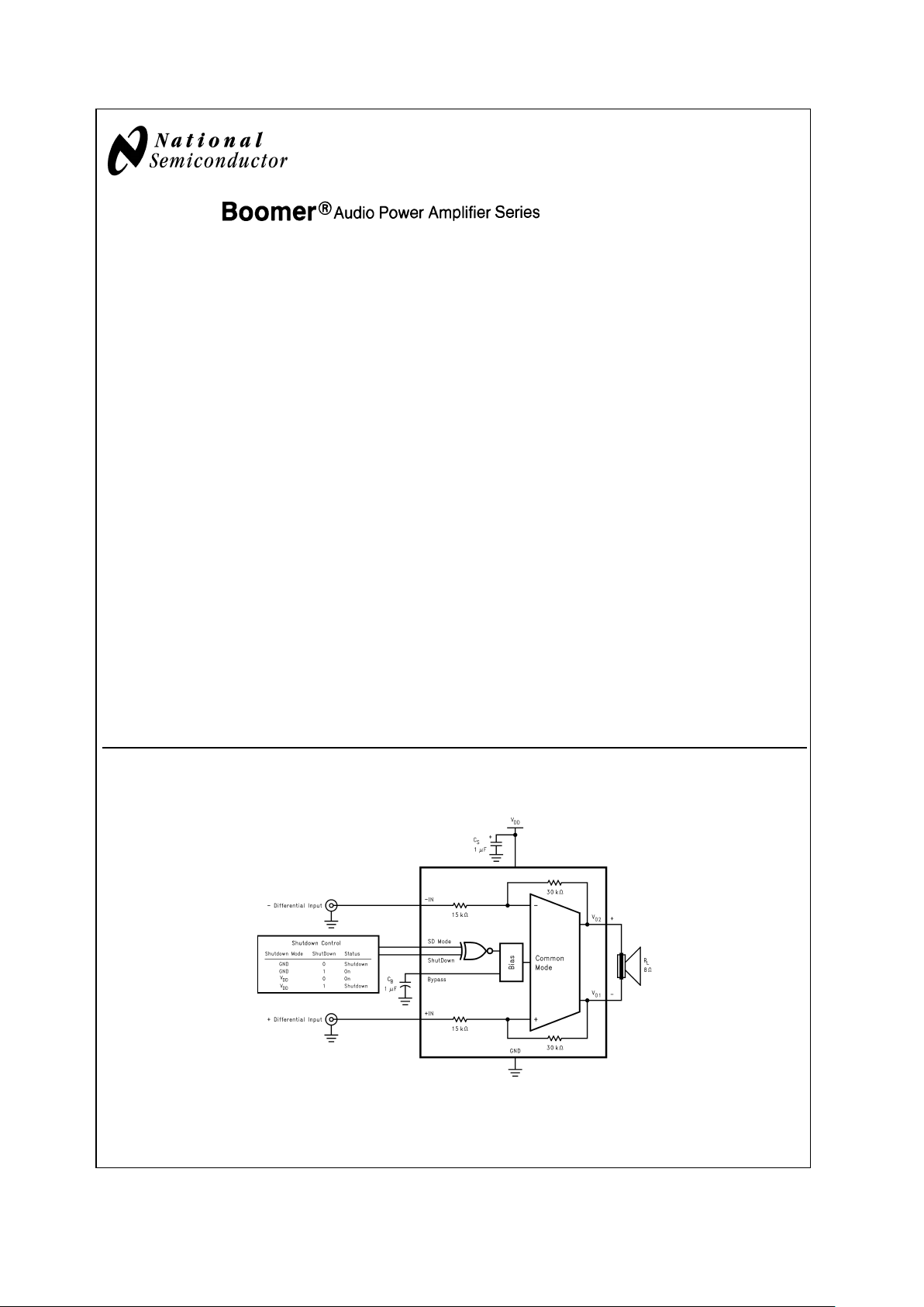
Typical Application
Boomer®is a registered trademark of National Semiconductor Corporation.
20023201
FIGURE 1. Typical Audio Amplifier Application Circuit
October 2002
LM4895 1 Watt Fully Differential Audio Power Amplifier With Shutdown Select and Fixed 6dB
Gain
© 2002 National Semiconductor Corporation DS200232 www.national.com
Page 2
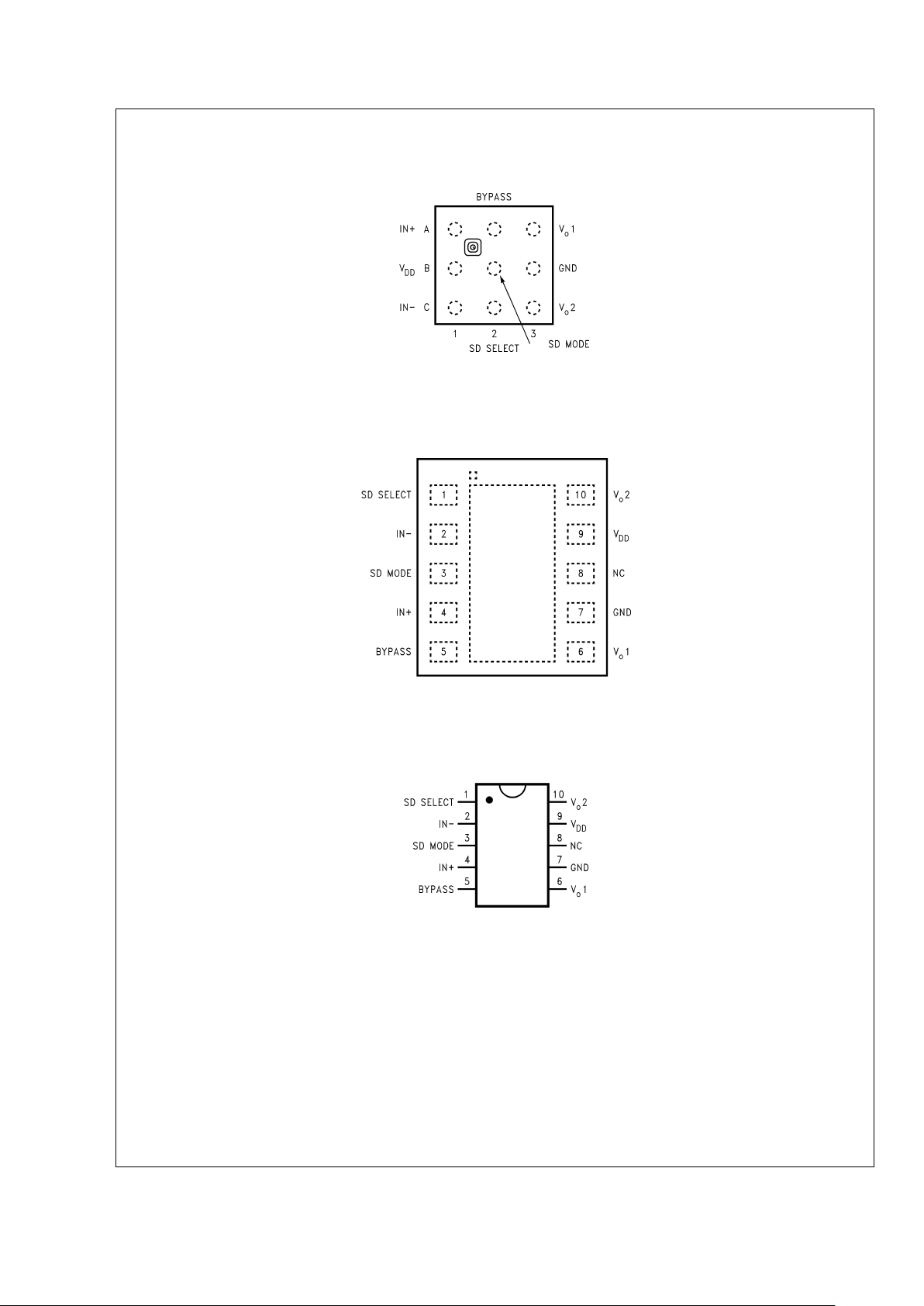
Connection Diagrams
9 Bump micro SMD Package
20023236
Top View
Order Number LM4895IBP
See NS Package Number BPA09CDB
LLP Package
20023235
Top View
Order Number LM4895LD
See NS Package Number LDA10B
Mini Small Outline (MSOP) Package
20023223
Top View
Order Number LM4895MM
See NS Package Number MUB10A
LM4895
www.national.com 2
Page 3
Absolute Maximum Ratings (Note 2)
If Military/Aerospace specified devices are required,
please contact the National Semiconductor Sales Office/
Distributors for availability and specifications.
Supply Voltage 6.0V
Storage Temperature −65˚C to +150˚C
Input Voltage −0.3V to V
DD
+0.3V
Power Dissipation (Note 3) Internally Limited
ESD Susceptibility (Note 4) 2000V
ESD Susceptibility (Note 5) 200V
Junction Temperature 150˚C
Thermal Resistance
θ
JC
(LD) 12˚C/W
θ
JA
(LD) 63˚C/W
θ
JA
(micro SMD) 220˚C/W
θ
JC
(MSOP) 56˚C/W
θ
JA
(MSOP) 190˚C/W
Soldering Information
See AN-1112 ’microSMD Wafers Level Chip Scale
Package’.
See AN-1187 ’Leadless
Leadframe Package (LLP)’.
Operating Ratings
Temperature Range
T
MIN
≤ TA≤ T
MAX
−40˚C ≤ TA≤ 85˚C
Supply Voltage 2.2V ≤ V
DD
≤ 5.5V
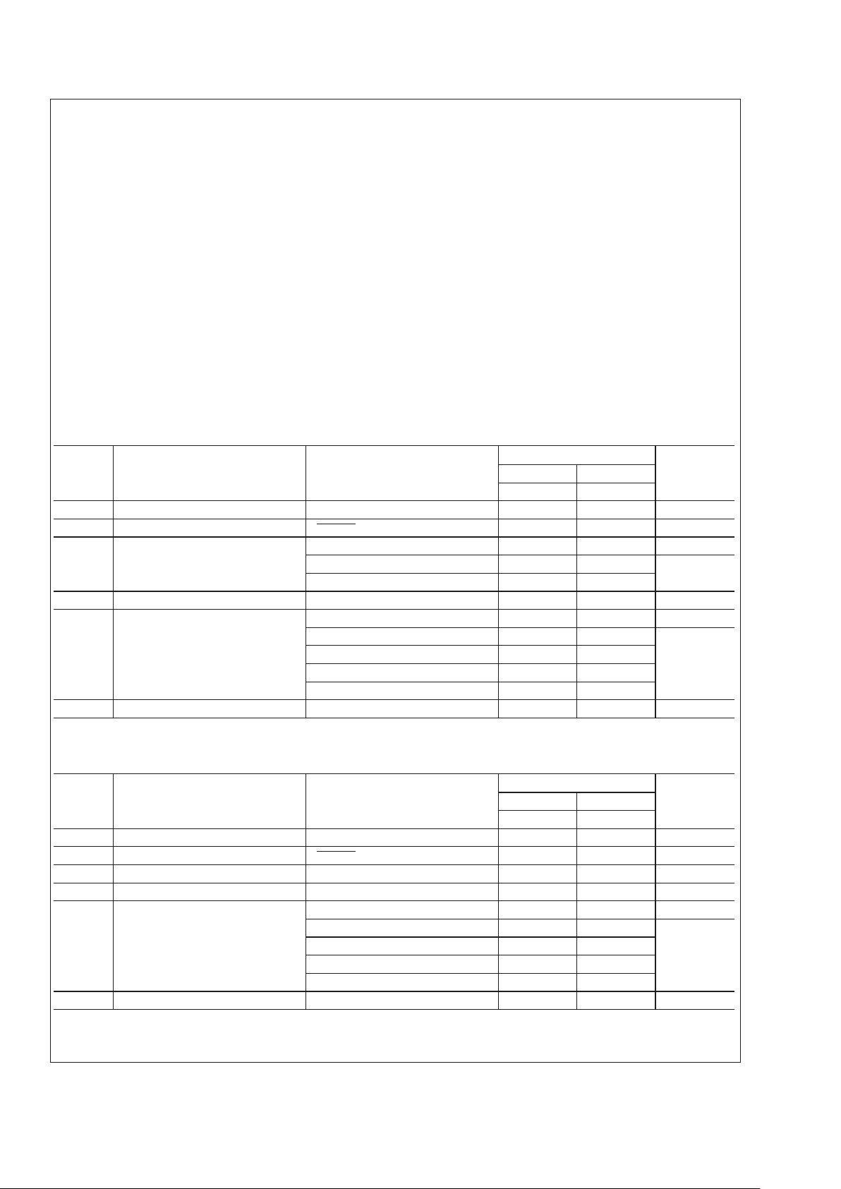
Electrical Characteristics VDD=5V (Notes 1, 2, 8)
The following specifications apply for V
DD
= 5V and 8Ω load unless otherwise specified. Limits apply for TA= 25˚C.
Symbol Parameter Conditions
LM4895
Units
(Limits)
Typical Limit
(Note 6) (Note 7)
I
DD
Quiescent Power Supply Current VIN= 0V, Io= 0A 4 8 mA (max)
I
SD
Shutdown Current V
shutdown
= GND 0.1 1 µA (max)
P
o
Output Power
THD = 1% (max);f=1kHz
LM4895LD, RL=4Ω (Note 11) 1.4 W (min)
LM4895, R
L
=8Ω 1 0.850
THD+N Total Harmonic Distortion+Noise P
o
= 0.4 Wrms; f = 1kHz 0.1 %
PSRR Power Supply Rejection Ratio
V
ripple
= 200mV sine p-p
f = 217Hz (Note 9) 84
dB (min)
f =1kHz (Note 9) 80
f = 217Hz (Note 10) 80 60
f =1kHz (Note 10) 77
CMRR Common-Mode Rejection Ratio f =217Hz 50 dB
Electrical Characteristics VDD=3V (Notes 1, 2, 8)
The following specifications apply for V
DD
= 3V and 8Ω load unless otherwise specified. Limits apply for TA= 25˚C.
Symbol Parameter Conditions
LM4895
Units
(Limits)
Typical Limit
(Note 6) (Note 7)
I
DD
Quiescent Power Supply Current VIN= 0V, Io= 0A 3.5 6 mA (max)
I
SD
Shutdown Current V
shutdown
= GND 0.1 1 µA (max)
P
o
Output Power THD = 1% (max); f = 1kHz 0.35 W
THD+N Total Harmonic Distortion+Noise P
o
= 0.25Wrms; f = 1kHz 0.325 %
PSRR Power Supply Rejection Ratio
V
ripple
= 200mV sine p-p
f = 217Hz (Note 9) 84
dB
f = 1kHz (Note 9) 80
f = 217Hz (Note 10) 77
f = 1kHz (Note 10) 75
CMRR Common-Mode Rejection Ratio f = 217Hz 49 dB
Note 1: All voltages are measured with respect to the ground pin, unless otherwise specified.
LM4895
www.national.com3
Page 4
Electrical Characteristics VDD=3V(Notes 1, 2, 8)
The following specifications apply for V
DD
= 3V and 8Ω load unless otherwise specified. Limits apply for TA=
25˚C. (Continued)
Note 2: Absolute Maximum Ratings indicate limits beyond which damage to the device may occur. Operating Ratings indicate conditions for which the device is
functional, but do not guarantee specific performance limits. Electrical Characteristics state DC andAC electrical specifications under particular test conditions which
guarantee specific performance limits. This assumes that the device is within the Operating Ratings. Specifications are not guaranteed for parameters where no limit
is given, however, the typical value is a good indication of device performance.
Note 3: The maximum power dissipation must be derated at elevated temperatures and is dictated by T
JMAX
, θJA, and the ambient temperature TA. The maximum
allowable power dissipation is P
DMAX
=(T
JMAX–TA
)/θJAor the number given inAbsolute Maximum Ratings, whichever is lower. For the LM4895, see power derating
currents for additional information.
Note 4: Human body model, 100pF discharged through a 1.5kΩ resistor.
Note 5: Machine Model, 220pF–240pF discharged through all pins.
Note 6: Typicals are measured at 25˚C and represent the parametric norm.
Note 7: Datasheet min/max specification limits are guaranteed by design, test, or statistical analysis.
Note 8: For micro SMD only, shutdown current is measured in a Normal Room Environment. Exposure to direct sunlight will increase I
SD
by a maximum of 2µA.
Note 9: Unterminated input.
Note 10: 10Ω terminated input.
Note 11: When driving 4Ω loads from a 5V supply, the LM4895LD must be mounted to a circuit board.
External Components Description (Figure 1)
Components Functional Description
1. C
S
Supply bypass capacitor which provides power supply filtering. Refer to the Power Supply Bypassing
section for information concerning proper placement and selection of the supply bypass capacitor.
2. C
B
Bypass pin capacitor which provides half-supply filtering. Refer to the section, Proper Selection of External
Components, for information concerning proper placement and selection of C
B
.
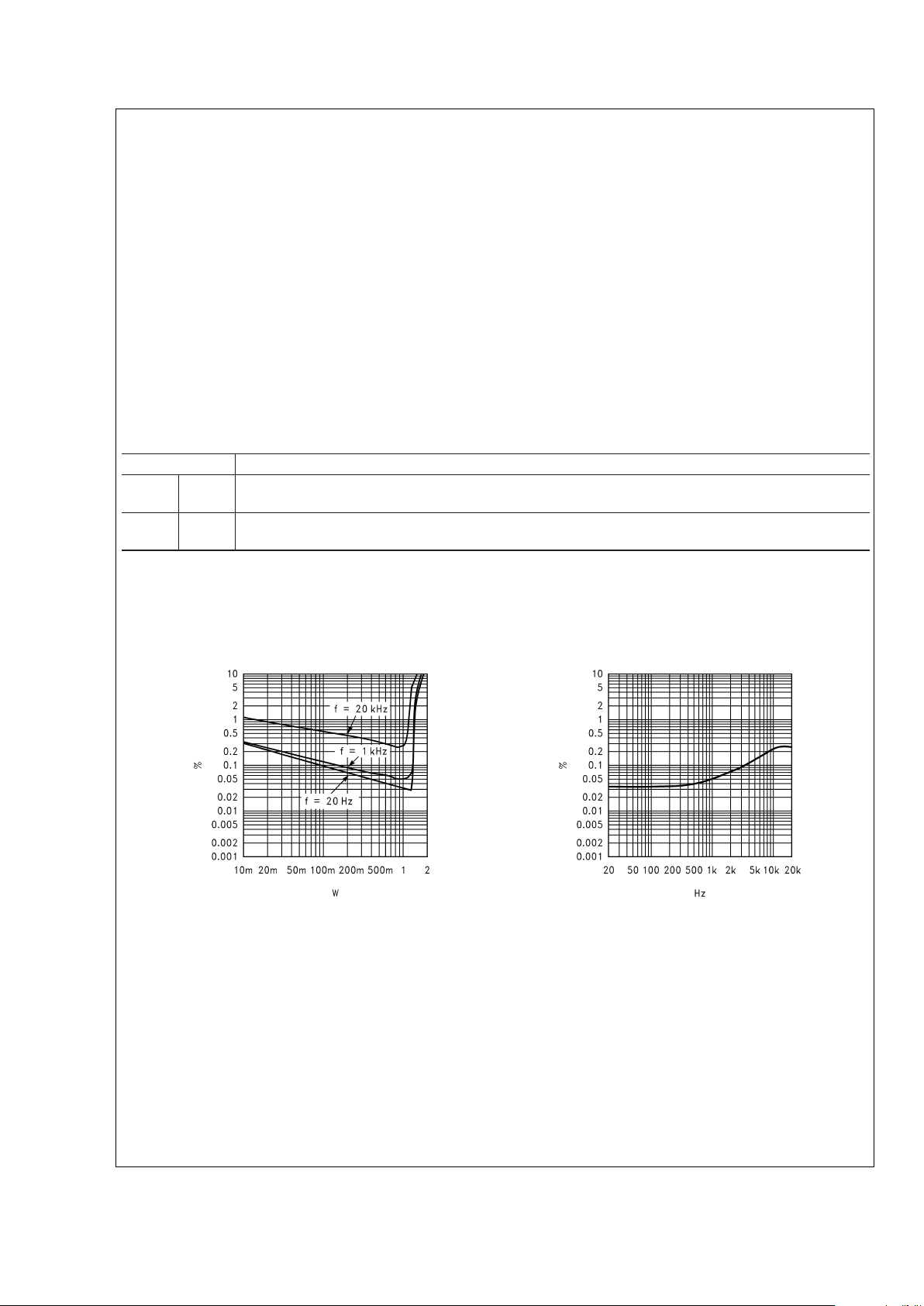
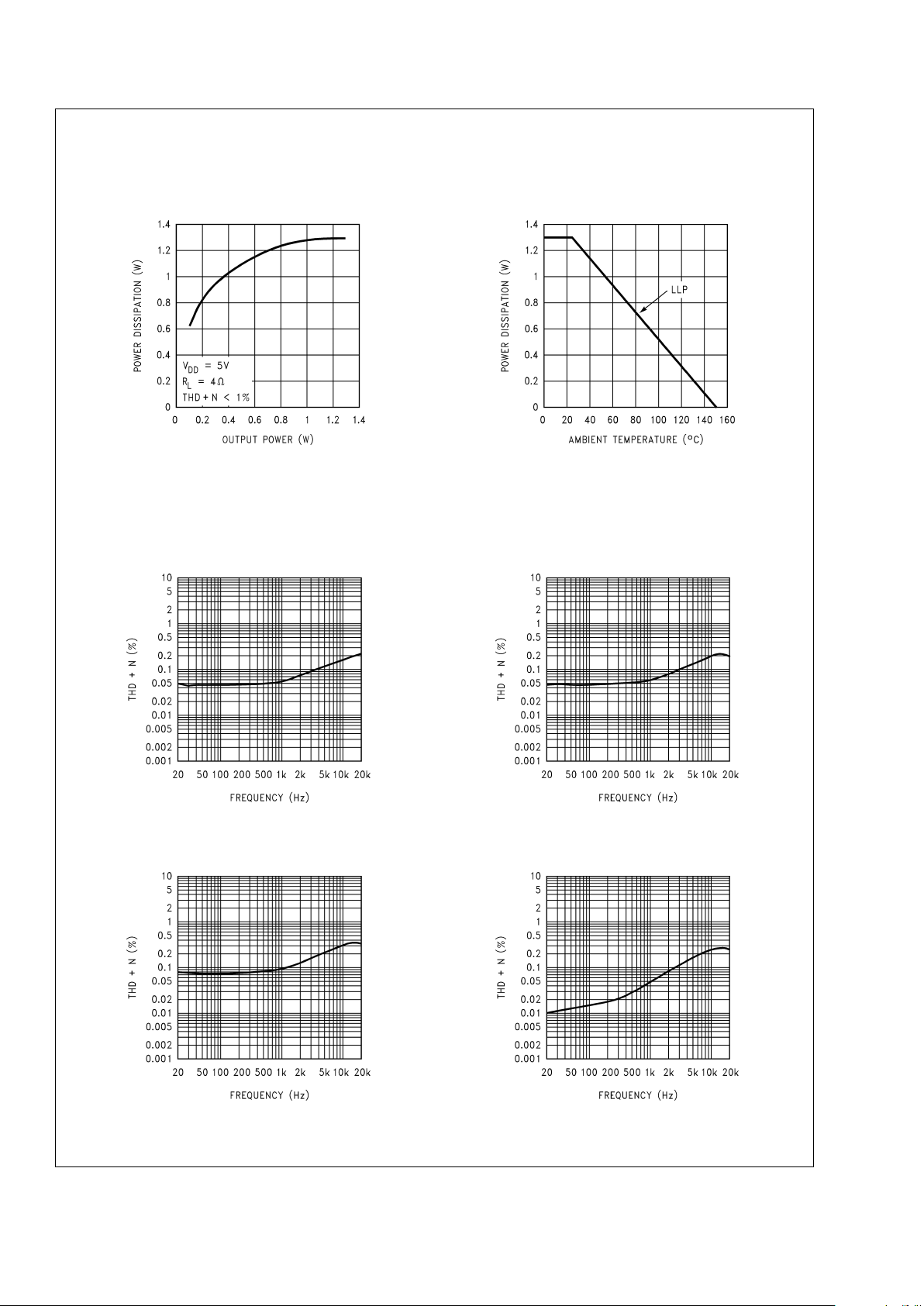
Typical Performance Characteristics
LD Specific Characteristics
LM4895LD
THD+N vs Output Power
V
DD
= 5V, 4Ω R
L
LM4895LD
THD+N vs Frequency
V
DD
= 5V, 4Ω RL, and Power = 1W
20023202 20023210
LM4895
www.national.com 4
Page 5
Typical Performance Characteristics
LD Specific Characteristics
(Continued)
LM4895LD
Power Dissipation vs Output Power
LM4895LD
Power Derating Curve
20023211 20023212
Typical Performance Characteristics
Non-LD Specific Characteristics
THD+N vs Frequency
at V
DD
= 5V, 8Ω RL, and PWR = 400mW
THD+N vs Frequency
VDD= 3V, 8Ω RL, and PWR = 250mW
20023213 20023230
THD+N vs Frequency
at V
DD
= 3V, 4Ω RL, and PWR = 225mW
THD+N vs Frequency
VDD= 2.6V, 8Ω RL, and PWR = 150mW
20023231 20023232
LM4895
www.national.com5
Page 6

Typical Performance Characteristics
Non-LD Specific Characteristics
(Continued)
THD+N vs Frequency
at V
DD
= 2.6V, 4Ω RL, and PWR = 150mW
THD+N vs Output Power
VDD= 5V, 8Ω R
L
20023233 20023234
THD+N vs Output Power
at V
DD
= 3V, 8Ω R
L
THD+N vs Output Power
V
DD
= 3V, 4Ω R
L
20023270 20023271
THD+N vs Output Power
at V
DD
= 2.6V, 8Ω R
L
THD+N vs Output Power
V
DD
= 2.6V, 4Ω R
L
20023272 20023274
LM4895
www.national.com 6
Page 7

Typical Performance Characteristics
Non-LD Specific Characteristics
(Continued)
Power Supply Rejection Ratio (PSRR) V
DD
=5V
Input 10Ω Terminated
Power Supply Rejection Ratio (PSRR) VDD=5V
Input Floating
20023275 20023276
Power Supply Rejection Ratio (PSRR) VDD=3V
Input 10Ω Terminated
Power Supply Rejection Ratio (PSRR) VDD=3V
Input Floating
20023277 20023278
Output Power vs
Supply Voltage
Output Power vs
Supply Voltage
20023279
20023280
LM4895
www.national.com7
Page 8

Typical Performance Characteristics
Non-LD Specific Characteristics
(Continued)
Power Dissipation vs
Output Power
Power Dissipation vs
Output Power
20023281 20023282
Power Dissipation vs
Output Power
Output Power vs
Load Resistance
20023283 20023284
Supply Current vs Shutdown Voltage
Shutdown Low
Supply Current vs Shutdown Voltage
Shutdown High
20023285 20023286
LM4895
www.national.com 8
Page 9

Typical Performance Characteristics
Non-LD Specific Characteristics
(Continued)
Clipping (Dropout) Voltage vs
Supply Voltage Open Loop Frequency Response
20023287
20023288
Power Derating Curve Noise Floor
20023289
20023290
Input CMRR vs Frequency Input CMRR vs Frequency
20023291 20023292
LM4895
www.national.com9
Page 10

Typical Performance Characteristics
Non-LD Specific Characteristics
(Continued)
PSRR vs
DC Common-Mode Voltage
PSRR vs
DC Common-Mode Voltage
20023293
20023294
THD vs
Common-Mode Voltage
THD vs
Common-Mode Voltage
20023295
20023296
LM4895
www.national.com 10
Page 11

Application Information
DIFFERENTIAL AMPLIFIER EXPLANATION
The LM4895 is a fully differential audio amplifier that features differential input and output stages. Internally this is
accomplished by two circuits: a differential amplifier and a
common mode feedback amplifier that adjusts the output
voltages so that the average value remains V
DD
/2. The
LM4895 features precisely matched internal gain-setting resistors, thus eliminating the need for external resistors and
fixing the differential gain at A
VD
= 6dB.
A differential amplifier works in a manner where the difference between the two input signals is amplified. In most
applications, this would require input signals that are 180˚
out of phase with each other.
The LM4895 provides what is known as a ’bridged mode’
output (bridge-tied-load, BTL). This results in output signals
at V
o1
and Vo2that are 180˚ out of phase with respect to
each other. Bridged mode operation is different from the
single-ended amplifier configuration that connects the load
between the amplifier output and ground. A bridged amplifier
design has distinct advantages over the single-ended configuration: it provides differential drive to the load, thus doubling maximum possible output swing for a specific supply
voltage. Four times the output power is possible compared
with a single-ended amplifier under the same conditions.
This increase in attainable output power assumes that the
amplifier is not current limited or clipped.
A bridged configuration, such as the one used in the
LM4895, also creates a second advantage over singleended amplifiers. Since the differential outputs, V
o1
and Vo2,
are biased at half-supply, no net DC voltage exists across
the load. BTL configuration eliminates the output coupling
capacitor required in single-supply, single-ended amplifier
configurations. If an output coupling capacitor is not used in
a single-ended output configuration, the half-supply bias
across the load would result in both increased internal IC
power dissipation as well as permanent loudspeaker damage. Further advantages of bridged mode operation specific
to fully differential amplifiers like the LM4895 include increased power supply rejection ratio, common-mode noise
reduction, and click and pop reduction.
EXPOSED-DAP PACKAGE PCB MOUNTING
CONSIDERATIONS
The LM4895’s exposed-DAP (die attach paddle) package
(LD) provide a low thermal resistance between the die and
the PCB to which the part is mounted and soldered. This
allows rapid heat transfer from the die to the surrounding
PCB copper traces, ground plane and, finally, surrounding
air. The result is a low voltage audio power amplifier that
produces 1.4W at ≤ 1% THD with a 4Ω load. This high power
is achieved through careful consideration of necessary thermal design. Failing to optimize thermal design may compromise the LM4895’s high power performance and activate
unwanted, though necessary, thermal shutdown protection.
The LD package must have its DAP soldered to a copper
pad on the PCB. The DAP’s PCB copper pad is connected to
a large plane of continuous unbroken copper. This plane
forms a thermal mass and heat sink and radiation area.
Place the heat sink area on either outside plane in the case
of a two-sided PCB, or on an inner layer of a board with more
than two layers. Connect the DAP copper pad to the inner
layer or backside copper heat sink area with 4 (2x2) vias.
The via diameter should be 0.012in - 0.013in with a 0.050in
pitch. Ensure efficient thermal conductivity by platingthrough and solder-filling the vias.
Best thermal performance is achieved with the largest practical copper heat sink area. If the heatsink and amplifier
share the same PCB layer, a nominal 2.5in
2
(min) area is
necessary for 5V operation with a 4Ω load. Heatsink areas
not placed on the same PCB layer as the LM4895 should be
5in
2
(min) for the same supply voltage and load resistance.
The last two area recommendations apply for 25˚C ambient
temperature. In all circumstances and conditions, the junction temperature must be held below 150˚C to prevent activating the LM4895’s thermal shutdown protection. The
LM4895’s power de-rating curve in the Typical Performance
Characteristics shows the maximum power dissipation versus temperature. Example PCB layouts for the exposedDAP TSSOP and LLP packages are shown in the Demonstration Board Layout section. Further detailed and specific
information concerning PCB layout, fabrication, and mounting an LLP package is available from National Semiconductor’s package Engineering Group under application note
AN-1187.
PCB LAYOUT AND SUPPLY REGULATION
CONSIDERATIONS FOR DRIVING 3Ω AND 4Ω LOADS
Power dissipated by a load is a function of the voltage swing
across the load and the load’s impedance. As load impedance decreases, load dissipation becomes increasingly dependent on the interconnect (PCB trace and wire) resistance
between the amplifier output pins and the load’s connections. Residual trace resistance causes a voltage drop,
which results in power dissipated in the trace and not in the
load as desired. For example, 0.1Ω trace resistance reduces
the output power dissipated by a 4Ω load from 1.4W to
1.37W. This problem of decreased load dissipation is exacerbated as load impedance decreases. Therefore, to maintain the highest load dissipation and widest output voltage
swing, PCB traces that connect the output pins to a load
must be as wide as possible.
Poor power supply regulation adversely affects maximum
output power. A poorly regulated supply’s output voltage
decreases with increasing load current. Reduced supply
voltage causes decreased headroom, output signal clipping,
and reduced output power. Even with tightly regulated supplies, trace resistance creates the same effects as poor
sup-ply regulation. Therefore, making the power supply
traces as wide as possible helps maintain full output voltage
swing.
POWER DISSIPATION
Power dissipation is a major concern when designing a
successful amplifer, whether the amplifier is bridged or
single-ended. Equation 2 states the maximum power dissipation point for a single-ended amplifier operating at a given
supply voltage and driving a specified output load.
P
DMAX
=(VDD)2/(2π2RL) Single-Ended (1)
LM4895
www.national.com11
Page 12

Application Information (Continued)
However, a direct consequence of the increased power delivered to the load by a bridge amplifier is an increase in
internal power dissipation versus a single-ended amplifier
operating at the same conditions.
P
DMAX
= 4*(VDD)2/(2π2RL) Bridge Mode (2)
Since the LM4895 has bridged outputs, the maximum internal power dissipation is 4 times that of a single-ended amplifier. Even with this substantial increase in power dissipation, the LM4895 does not require additional heatsinking
under most operating conditions and output loading. From
Equation 3, assuming a 5V power supply and an 8Ω load,
the maximum power dissipation point is 625mW. The maximum power dissipation point obtained from Equation 3 must
not be greater than the power dissipation results from Equation 4:
P
DMAX
=(T
JMAX-TA
)/θ
JA
(3)
The LM4895’s θ
JA
in an MUA10A package is 190˚C/W.
Depending on the ambient temperature, T
A
, of the system
surroundings, Equation 4 can be used to find the maximum
internal power dissipation supported by the IC packaging. If
the result of Equation 3 is greater than that of Equation 4,
then either the supply voltage must be decreased, the load
impedance increased, the ambient temperature reduced, or
the θ
JA
reduced with heatsinking. In many cases, larger
traces near the output, V
DD
, and GND pins can be used to
lower the θ
JA
. The larger areas of copper provide a form of
heatsinking allowing higher power dissipation. For the typical
application of a 5V power supply, with an 8Ω load, the
maximum ambient temperature possible without violating the
maximum junction temperature is approximately 30˚C provided that device operation is around the maximum power
dissipation point. Recall that internal power dissipation is a
function of output power. If typical operation is not around the
maximum power dissipation point, the LM4895 can operate
at higher ambient temperatures. Refer to the Typical Per-
formance Characteristics curves for power dissipation information.
POWER SUPPLY BYPASSING
As with any power amplifier, proper supply bypassing is
critical for low noise performance and high power supply
rejection ratio (PSRR). The capacitor location on both the
bypass and power supply pins should be as close to the
device as possible. A larger half-supply bypass capacitor
improves PSRR because it increases half-supply stability.
Typical applications employ a 5V regulator with 10µF and
0.1µF bypass capacitors that increase supply stability. This,
however, does not eliminate the need for bypassing the
supply nodes of the LM4895. Although the LM4895 will
operate without the bypass capacitor C
B
, although the PSRR
may decrease. A 1µF capacitor is recommended for C
B
. This
value maximizes PSRR performance. Lesser values may be
used, but PSRR decreases at frequencies below 1kHz. The
issue of C
B
selection is thus dependant upon desired PSRR
and click and pop performance.
SHUTDOWN FUNCTION
In order to reduce power consumption while not in use, the
LM4895 contains shutdown circuitry that is used to turn off
the amplifier’s bias circuitry. In addition, the LM4895 contains a Shutdown Mode pin, allowing the designer to designate whether the part will be driven into shutdown with a high
level logic signal or a low level logic signal. This allows the
designer maximum flexibility in device use, as the Shutdown
Mode pin may simply be tied permanently to either V
DD
or
GND to set the LM4895 as either a ’shutdown-high’ device or
a ’shutdown-low’ device, respectively. The device may then
be placed into shutdown mode by toggling the Shutdown
Select pin to the same state as the Shutdown Mode pin. For
simplicity’s sake, this is called ’shutdown same’, as the
LM4895 enters shutdown mode whenever the two pins are
in the same logic state. The trigger point for either shutdown
high or shutdown low is shown as a typical value in the
Supply Current vs Shutdown Voltage graphs in the Typical
Performance Characteristics section. It is best to switch
between ground and supply for maximum performance.
While the device may be disabled with shutdown voltages in
between ground and supply, the idle current may be greater
than the typical value of 0.1µA. In either case, the shutdown
pin should be tied to a definite voltage to avoid unwanted
state changes.
In many applications, a microcontroller or microprocessor
output is used to control the shutdown circuitry, which provides a quick, smooth transition to shutdown. Another solution is to use a single-throw switch in conjunction with an
external pull-up resistor (or pull-down, depending on shutdown high or low application). This scheme guarantees that
the shutdown pin will not float, thus preventing unwanted
state changes.
LM4895
www.national.com 12
Page 13

Physical Dimensions inches (millimeters)
unless otherwise noted
9-Bump micro SMD
Order Number LM4895IBP
NS Package Number BPA09CDB
X1 = 1.336
±
0.03 X2 = 1.361±0.03 X3 = 0.850±0.10
LM4895
www.national.com13
Page 14

Physical Dimensions inches (millimeters) unless otherwise noted (Continued)
LLP
Order Number LM4895LD
NSPackage Number LDA10B
LM4895
www.national.com 14
Page 15

Physical Dimensions inches (millimeters) unless otherwise noted (Continued)
Mini Small Outline (MSOP)
Order Number LM4895MM
NSPackage Number MUB10A
LIFE SUPPORT POLICY
NATIONAL’S PRODUCTS ARE NOT AUTHORIZED FOR USE AS CRITICAL COMPONENTS IN LIFE SUPPORT
DEVICES OR SYSTEMS WITHOUT THE EXPRESS WRITTEN APPROVAL OF THE PRESIDENT AND GENERAL
COUNSEL OF NATIONAL SEMICONDUCTOR CORPORATION. As used herein:
1. Life support devices or systems are devices or
systems which, (a) are intended for surgical implant
into the body, or (b) support or sustain life, and
whose failure to perform when properly used in
accordance with instructions for use provided in the
labeling, can be reasonably expected to result in a
significant injury to the user.
2. A critical component is any component of a life
support device or system whose failure to perform
can be reasonably expected to cause the failure of
the life support device or system, or to affect its
safety or effectiveness.
National Semiconductor
Corporation
Americas
Email: support@nsc.com
National Semiconductor
Europe
Fax: +49 (0) 180-530 85 86
Email: europe.support@nsc.com
Deutsch Tel: +49 (0) 69 9508 6208
English Tel: +44 (0) 870 24 0 2171
Français Tel: +33 (0) 1 41 91 8790
National Semiconductor
Asia Pacific Customer
Response Group
Tel: 65-2544466
Fax: 65-2504466
Email: ap.support@nsc.com
National Semiconductor
Japan Ltd.
Tel: 81-3-5639-7560
Fax: 81-3-5639-7507
www.national.com
LM4895 1 Watt Fully Differential Audio Power Amplifier With Shutdown Select and Fixed 6dB
Gain
National does not assume any responsibility for use of any circuitry described, no circuit patent licenses are implied and National reserves the right at any time without notice to change said circuitry and specifications.
 Loading...