

Page 1
LM4890
1 Watt Audio Power Amplifier
General Description
The LM4890 is an audio power amplifier primarily designed
for demanding applications in mobile phones and other portable communication device applications. It is capable of
delivering 1 watt of continuous average power to an 8Ω BTL
load with less than 1% distortion (THD+N) from a 5V
DC
power supply.
Boomer audio power amplifiers were designed specifically to
provide high quality output power with a minimal amount of
external components. The LM4890 does not require output
coupling capacitors or bootstrap capacitors, and therefore is
ideally suited for mobile phone and other low voltage applications where minimal power consumption is a primary requirement.
The LM4890 features a low-power consumption shutdown
mode, which is achieved by driving the shutdown pin with
logic low. Additionally, the LM4890 features an internal thermal shutdown protection mechanism.
The LM4890 contains advanced pop & click circuitry which
eliminates noises which would otherwise occur during
turn-on and turn-off transitions.
The LM4890 is unity-gain stable and can be configured by
external gain-setting resistors.
Key Specifications
j
PSRR at 217Hz, VDD= 5V (Fig. 1) 62dB(typ.)
j
Power Output at 5.0V & 1% THD 1W(typ.)
j
Power Output at 3.3V & 1% THD 400mW(typ.)
j
Shutdown Current 0.1µA(typ.)
Features
n Available in space-saving packages: micro SMD, MSOP,
SOIC, and LLP
n Ultra low current shutdown mode
n BTL output can drive capacitive loads
n Improved pop & click circuitry eliminates noises during
turn-on and turn-off transitions
n 2.2 - 5.5V operation
n No output coupling capacitors, snubber networks or
bootstrap capacitors required
n Thermal shutdown protection
n Unity-gain stable
n External gain configuration capability
Applications
n Mobile Phones
n PDAs
n Portable electronic devices
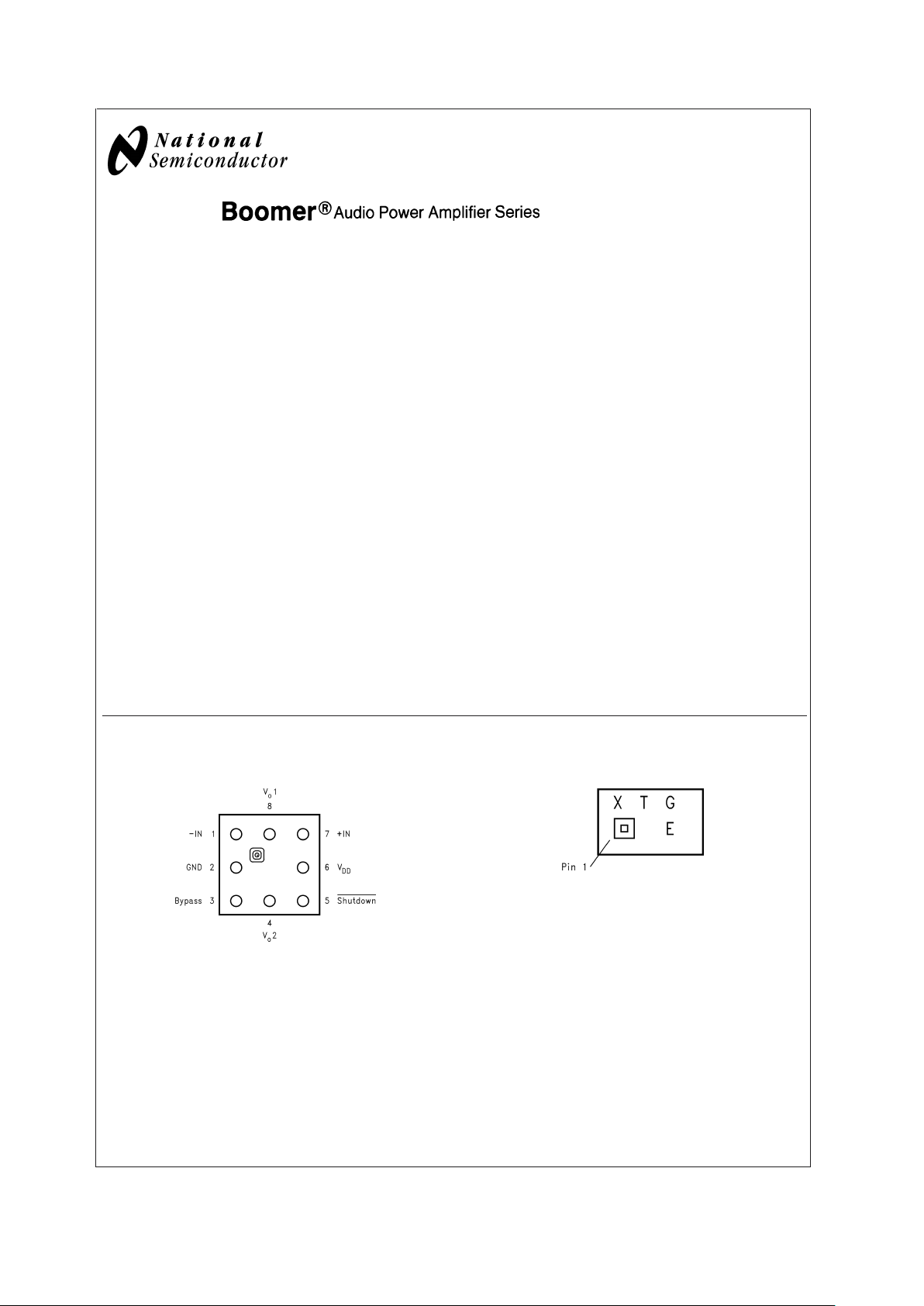
Connection Diagrams
8 Bump micro SMD 8 bump micro SMD Marking
20019223
Top View
Order Number LM4890IBP, LM4890IBPX
See NS Package Number BPA08DDB
20019270
Top View
X - Date Code
T - Die Traceability
G - Boomer Family
E - LM4890IBP
Boomer®is a registered trademark of National Semiconductor Corporation.
May 2003
LM4890 1 Watt Audio Power Amplifier
© 2003 National Semiconductor Corporation DS200192 www.national.com
Page 2
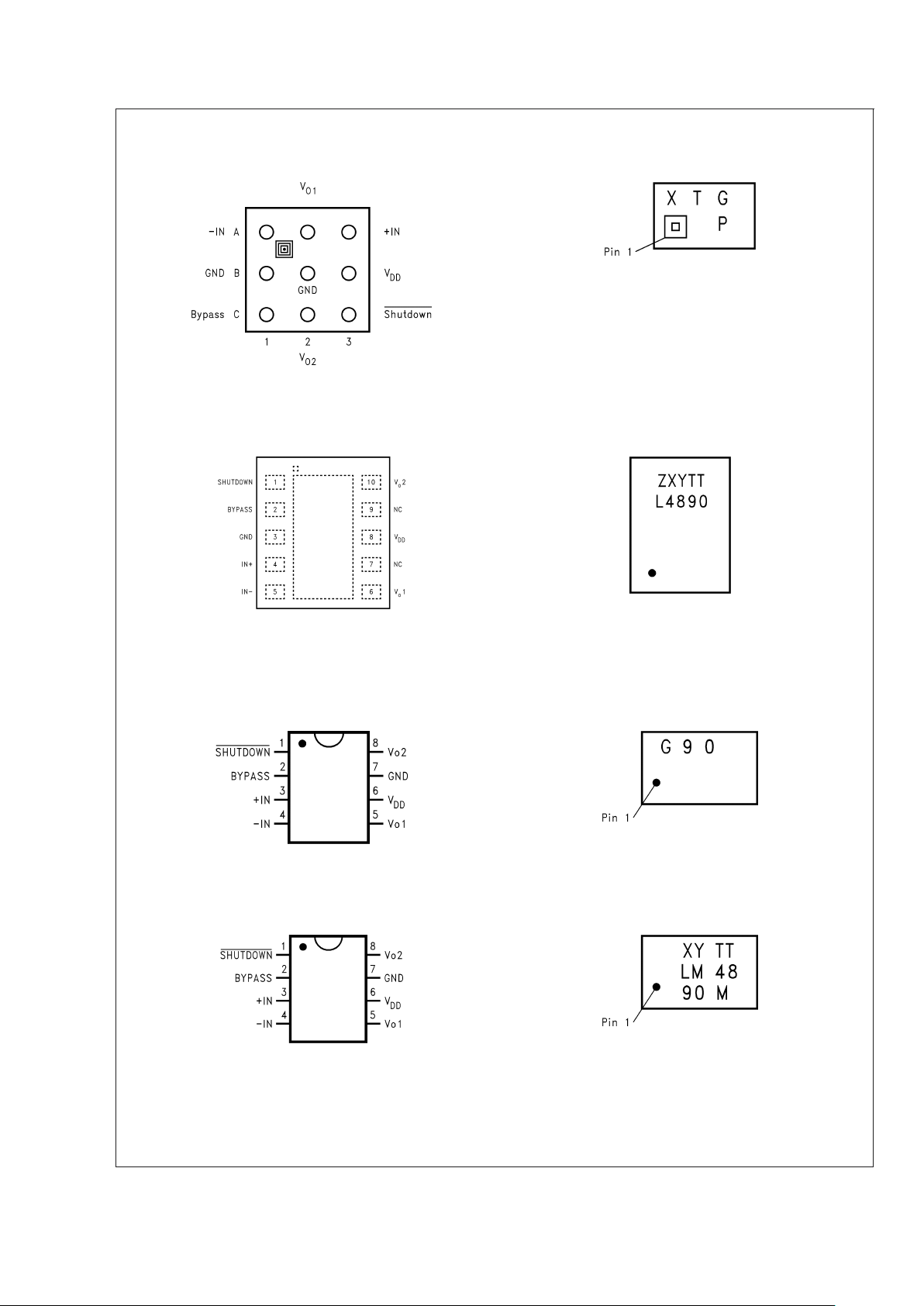
Connection Diagrams (Continued)
9 Bump micro SMD 9 Bump micro SMD Marking
200192C1
Top View
Order Number LM4890IBL, LM4890IBLX
See NS Package Number BLA09AAB
200192C2
Top View
X - Date Code
T - Die Traceability
G - Boomer Family
P - LM4890IBL
LLP Package 10 Pin LLP Marking
200192C7
Top View
Order Number LM4890LD
See NS Package Number LDA10B
200192C6
Top View
Z - Assembly Plant Date Code (M for Malacca)
XY - Digit Date Code
TT - Die Traceability
L4890 - LM4890LD
Mini Small Outline (MSOP) Package MSOP Marking
20019236
Top View
Order Number LM4890MM
See NS Package Number MUA08A
20019271
Top View
G - Boomer Family
90 - LM4890MM
Small Outline (SO) Package SO Marking
20019235
Top View
Order Number LM4890M
See NS Package Number M08A
20019272
Top View
XY - Date Code
TT - Die Traceability
Bottom 2 lines - Part Number
LM4890
www.national.com 2
Page 3
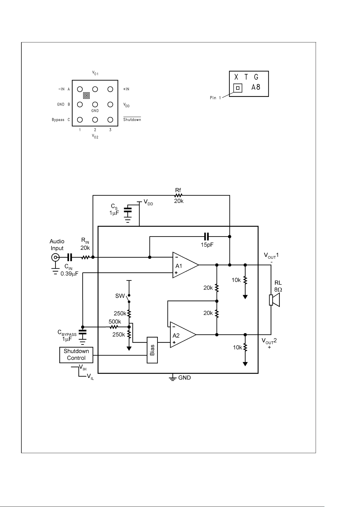
Connection Diagrams (Continued)
9 Bump micro SMD 9 Bump micro SMD Marking
200192C1
Top View
Order Number LM4890ITL, LM4890ITLX
See NS Package Number TLA09AAA
200192D0
Top View
X - Date Code
T - Die Traceability
G - Boomer Family
A8 - LM4890ITL
Typical Application
20019201
FIGURE 1. Typical Audio Amplifier Application Circuit
LM4890
www.national.com3
Page 4
Absolute Maximum Ratings (Note 2)
If Military/Aerospace specified devices are required,
please contact the National Semiconductor Sales Office/
Distributors for availability and specifications.
Supply Voltage (Note 11) 6.0V
Storage Temperature −65˚C to +150˚C
Input Voltage −0.3V to V
DD
+0.3V
Power Dissipation (Note 3) Internally Limited
ESD Susceptibility (Note 4) 2000V
Junction Temperature 150˚C
Thermal Resistance
θ
JC
(SOP) 35˚C/W
θ
JA
(SOP) 150˚C/W
θ
JA
(8 Bump micro SMD, Note 12) 220˚C/W
θ
JA
(9 Bump micro SMD, Note 12) 180˚C/W
θ
JC
(MSOP) 56˚C/W
θ
JA
(MSOP) 190˚C/W
θ
JA
(LLP) 220˚C/W
Soldering Information
See AN-1112 "microSMD Wafers Level Chip Scale
Package."
See AN-1187 "Leadless Leadframe Package (LLP)."
Operating Ratings
Temperature Range
T
MIN
≤ TA≤ T
MAX
−40˚C ≤ TA≤ 85˚C
Supply Voltage 2.2V ≤ V
DD
≤ 5.5V
Electrical Characteristics VDD=5V (Notes 1, 2, 8)
The following specifications apply for the circuit shown in Figure 1 unless otherwise specified. Limits apply for T
A
= 25˚C.
Symbol Parameter Conditions
LM4890
Units
(Limits)
Typical Limit
(Note 6) (Notes 7, 9)
I
DD
Quiescent Power Supply Current VIN= 0V, Io= 0A, No Load 4 8 mA (max)
V
IN
= 0V, Io= 0A, 8Ω Load 5 10 mA (max)
I
SD
Shutdown Current V
SHUTDOWN
= 0V 0.1 2.0 µA (max)
V
SDIH
Shutdown Voltage Input High 1.2 V (min)
V
SDIL
Shutdown Voltage Input Low 0.4 V (max)
V
OS
Output Ofsett Voltage 7 50 mV (max)
R
OUT-GND
Resistor Output to GND (Note 10)
8.5
9.7 kΩ (max)
7.0 kΩ (min)
P
o
Output Power ( 8Ω ) THD = 2% (max);f=1kHz 1.0 0.8 W
T
WU
Wake-up time 170 220 ms (max)
T
SD
Thermal Shutdown Temperature
170
150 ˚C (min)
190 ˚C (max)
THD+N Total Harmonic Distortion+Noise P
o
= 0.4 Wrms; f = 1kHz 0.1 %
PSRR Power Supply Rejection Ratio
(Note 14)
V
ripple
= 200mV sine p-p
Input Terminated with 10 ohms to
ground
62 (f =
217Hz)
66 (f = 1kHz)
55 dB (min)
T
SDT
Shut Down Time 8 Ω load 1.0 ms (max)
Electrical Characteristics VDD=3V (Notes 1, 2, 8)
The following specifications apply for the circuit shown in Figure 1 unless otherwise specified. Limits apply for T
A
= 25˚C.
Symbol Parameter Conditions
LM4890
Units
(Limits)
Typical Limit
(Note 6) (Notes 7, 9)
I
DD
Quiescent Power Supply Current VIN= 0V, Io= 0A, No Load 3.5 7 mA (max)
V
IN
= 0V, Io= 0A, 8Ω Load 4.5 9 mA (max)
I
SD
Shutdown Current V
SHUTDOWN
= 0V 0.1 2.0 µA (max)
V
SDIH
Shutdown Voltage Input High 1.2 V(min)
V
SDIL
Shutdown Voltage Input Low 0.4 V(max)
V
OS
Output Offset Voltage 7 50 mV (max)
R
OUT-GND
Resistor Output to Gnd (Note 10)
8.5
9.7 kΩ (max)
7.0 kΩ (min)
T
WU
Wake-up time 120 180 ms (max)
LM4890
www.national.com 4
Page 5
Electrical Characteristics VDD=3V(Notes 1, 2, 8)
The following specifications apply for the circuit shown in Figure 1 unless otherwise specified. Limits apply for T
A
=
25˚C. (Continued)
Symbol Parameter Conditions
LM4890
Units
(Limits)
Typical Limit
(Note 6) (Notes 7, 9)
P
o
Output Power ( 8Ω ) THD = 1% (max); f = 1kHz 0.31 0.28 W
T
SD
Thermal Shutdown Temperature
170
150 ˚C(min)
190 ˚C(max)
THD+N Total Harmonic Distortion+Noise P
o
= 0.15Wrms; f = 1kHz 0.1 %
PSRR Power Supply Rejection Ratio
(Note 14)
V
ripple
= 200mV sine p-p
Input terminated with 10 ohms to
ground
56 (f =
217Hz)
62 (f = 1kHz)
45 dB(min)
Electrical Characteristics VDD= 2.6V (Notes 1, 2, 8)
The following specifications apply for for the circuit shown in Figure 1 unless otherwise specified. Limits apply for T
A
= 25˚C.
Symbol Parameter Conditions
LM4890
Units
(Limits)
Typical Limit
(Note 6) (Notes 7, 9)
I
DD
Quiescent Power Supply Current VIN= 0V, Io= 0A, No Load 2.6 mA (max)
I
SD
Shutdown Current V
SHUTDOWN
= 0V 0.1 µA (max)
P
0
Output Power ( 8Ω )
Output Power ( 4Ω )
THD = 1% (max);f=1kHz
THD = 1% (max);f=1kHz
0.2
0.22
W
W
THD+N Total Harmonic Distortion+Noise P
o
= 0.1Wrms; f = 1kHz 0.08 %
PSRR Power Supply Rejection Ratio
(Note 14)
V
ripple
= 200mV sine p-p
Input Terminated with 10 ohms to
ground
44 (f =
217Hz)
44 (f = 1kHz)
dB
Note 1: All voltages are measured with respect to the ground pin, unless otherwise specified.
Note 2: Absolute Maximum Ratings indicate limits beyond which damage to the device may occur. Operating Ratings indicate conditions for which the device is
functional, but do not guarantee specific performance limits. Electrical Characteristics state DC andAC electrical specifications under particular test conditions which
guarantee specific performance limits. This assumes that the device is within the Operating Ratings. Specifications are not guaranteed for parameters where no limit
is given, however, the typical value is a good indication of device performance.
Note 3: The maximum power dissipation must be derated at elevated temperatures and is dictated by T
JMAX
, θJA, and the ambient temperature TA. The maximum
allowable power dissipation is P
DMAX
=(T
JMAX–TA
)/θJAor the number given inAbsolute Maximum Ratings, whichever is lower. For the LM4890, see power derating
curves for additional information.
Note 4: Human body model, 100 pF discharged through a 1.5 kΩ resistor.
Note 5: Machine Model, 220 pF–240 pF discharged through all pins.
Note 6: Typicals are measured at 25˚C and represent the parametric norm.
Note 7: Limits are guaranteed to National’s AOQL (Average Outgoing Quality Level).
Note 8: For micro SMD only, shutdown current is measured in a Normal Room Environment. Exposure to direct sunlight will increase I
SD
by a maximum of 2µA.
Note 9: Datasheet min/max specification limits are guaranteed by design, test, or statistical analysis.
Note 10: ROUT is measured from each of the output pins to ground. This value represents the parallel combination of the 10k ohm output resistors and the two 20k
ohm resistors.
Note 11: If the product is in shutdown mode and V
DD
exceeds 6V (to a max of 8V VDD), then most of the excess current will flow through the ESD protection circuits.
If the source impedance limits the current to a max of 10 ma, then the part will be protected. If the part is enabled when V
DD
is greater than 5.5V and less than 6.5V,
no damage will occur, although operational life will be reduced. Operation above 6.5V with no current limit will result in permanent damage.
Note 12: All bumps have the same thermal resistance and contribute equally when used to lower thermal resistance. All bumps must be connected to achieve
specified thermal resistance.
Note 13: Maximum power dissipation (P
DMAX
) in the device occurs at an output power level significantly below full output power. P
DMAX
can be calculated using
Equation 1 shown in the Application section. It may also be obtained from the power dissipation graphs.
Note 14: PSRR is a function of system gain. Specifications apply to the circuit in Figure 1 where A
V
= 2. Higher system gains will reduce PSRR value by the amount
of gain increase. A system gain of 10 represents a gain increase of 14dB. PSRR will be reduced by 14dB and applies to all operating voltages.
LM4890
www.national.com5
Page 6

External Components Description (Figure 1)
Components Functional Description
1. R
IN
Inverting input resistance which sets the closed-loop gain in conjunction with Rf. This resistor also forms a
high pass filter with C
IN
at fC= 1/(2π RINCIN).
2. C
IN
Input coupling capacitor which blocks the DC voltage at the amplifier’s input terminals. Also creates a
highpass filter with R
IN
at fc= 1/(2π RINCIN). Refer to the section, Proper Selection of External
Components, for an explanation of how to determine the value of C
IN
.
3. R
f
Feedback resistance which sets the closed-loop gain in conjunction with RIN.
4. C
S
Supply bypass capacitor which provides power supply filtering. Refer to the section, Power Supply
Bypassing, for information concerning proper placement and selection of the supply bypass capacitor,
C
BYPASS
.
5. C
BYPASS
Bypass pin capacitor which provides half-supply filtering. Refer to the section, Proper Selection of External
Components, for information concerning proper placement and selection of C
BYPASS
.
LM4890
www.national.com 6
Page 7
Typical Performance Characteristics
THD+N vs Frequency
at V
DD
= 5V, 8Ω RL, and PWR = 250mW, AV=2
THD+N vs Frequency
at VDD= 3.3V, 8Ω RL, and PWR = 150mW, AV=2
20019237 20019238
THD+N vs Frequency
at V
DD
= 3V, RL=8Ω, PWR = 250mW, AV=2
20019290
THD+N vs Frequency
@
VDD= 2.6V, RL=8Ω, PWR = 100mW, AV=2
THD+N vs Frequency
@
VDD= 2.6V, RL=4Ω, PWR = 100mW, AV=2
20019239 20019240
LM4890
www.national.com7
Page 8
Typical Performance Characteristics (Continued)
THD+N vs Power Out
@
VDD= 5V, RL=8Ω, 1kHz, AV=2
THD+N vs Power Out
@
VDD= 3.3V, RL=8Ω, 1kHz, AV=2
200192C9
20019242
THD+N vs Power Out
@
VDD= 3V, RL=8Ω, 1kHz, AV=2
20019291
THD+N vs Power Out
@
VDD= 2.6V, RL=8Ω, 1kHz, AV=2
THD+N vs Power Out
@
VDD= 2.6V, RL=4Ω, 1kHz, AV=2
20019243 20019244
LM4890
www.national.com 8
Page 9
Typical Performance Characteristics (Continued)
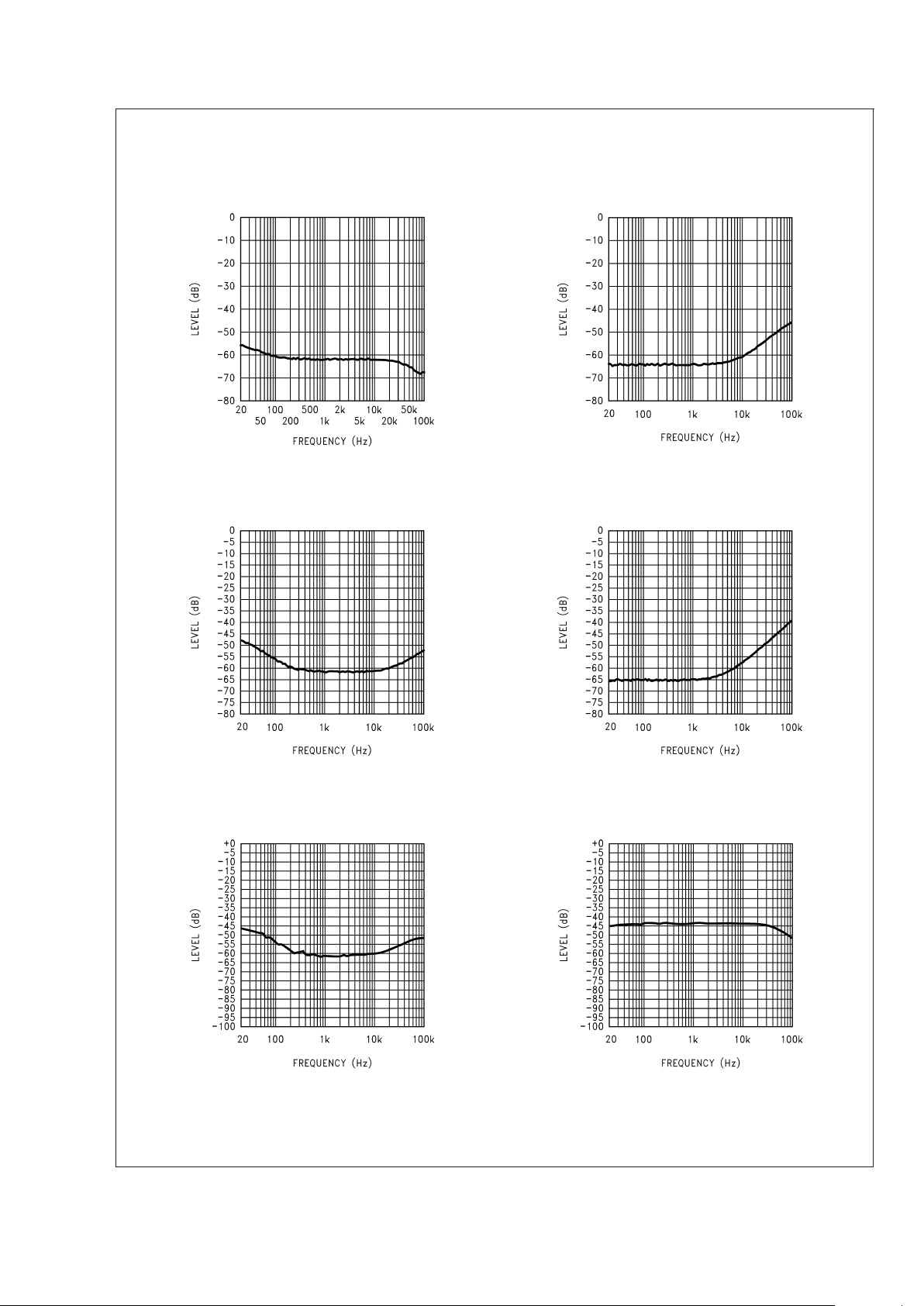
Power Supply Rejection Ratio (PSRR)
@
AV=2
V
DD
= 5V, V
ripple
= 200mvp-p
R
L
=8Ω,RIN=10Ω
Power Supply Rejection Ratio (PSRR)
@
AV=2
V
DD
= 5V, V
ripple
= 200mvp-p
R
L
=8Ω,RIN= Float
20019245 20019273
Power Supply Rejection Ratio (PSRR)@AV=4
V
DD
= 5V, V
ripple
= 200mvp-p
R
L
=8Ω,RIN=10Ω
Power Supply Rejection Ratio (PSRR)
@
AV=4
V
DD
= 5V, V
ripple
= 200mvp-p
R
L
=8Ω,RIN= Float
200192A9 200192B8
LM4890
www.national.com9
Page 10
Typical Performance Characteristics (Continued)
Power Supply Rejection Ratio (PSRR)
@
AV=2
V
DD
= 3V, V
ripple
= 200mvp-p,
R
L
=8Ω,RIN=10Ω
Power Supply Rejection Ratio (PSRR)
@
AV=2
V
DD
= 3V, V
ripple
= 200mvp-p,
R
L
=8Ω,RIN= Float
200192C5
20019293
Power Supply Rejection Ratio (PSRR)@AV=4
V
DD
= 3V, V
ripple
= 200mvp-p,
R
L
=8Ω,RIN=10Ω
Power Supply Rejection Ratio (PSRR)
@
AV=4
V
DD
= 3V, V
ripple
= 200mvp-p,
R
L
=8Ω,RIN= Float
200192B1 200192B9
Power Supply Rejection Ratio (PSRR)@AV=2
V
DD
= 3.3V, V
ripple
= 200mvp-p,
R
L
=8Ω,RIN=10Ω
Power Supply Rejection Ratio (PSRR)
@
AV=2
V
DD
= 2.6V, V
ripple
= 200mvp-p,
R
L
=8Ω,RIN=10Ω
20019246 20019247
LM4890
www.national.com 10
Page 11

Typical Performance Characteristics (Continued)
PSRR vs DC Output Voltage
V
DD
= 5V, AV=2
PSRR vs DC Output Voltage
VDD= 5V, AV=4
20019296
20019297
PSRR vs DC Output Voltage
V
DD
= 5V, AV=10
PSRR vs DC Output Voltage
VDD= 3V, AV=2
200192A3
20019294
PSRR vs DC Output Voltage
V
DD
= 3V, AV=4
PSRR vs DC Output Voltage
VDD= 3V, AV=10
20019295 200192A4
LM4890
www.national.com11
Page 12

Typical Performance Characteristics (Continued)
PSRR Distribution V
DD
=5V
217Hz, 200mvp-p,
-30, +25, and +80˚C
PSRR Distribution VDD=3V
217Hz, 200mvp-p,
-30, +25, and +80˚C
200192B4
200192B5
Power Supply Rejection Ration vs
Bypass Capacitor Size
V
DD
= 5V, Input Grounded = 10Ω, Output Load = 8Ω
Power Supply Rejection Ration vs
Bypass Capacitor Size
VDD= 3V, Input Grounded = 10Ω, Output Load = 8Ω
200192A7
Top Trace = No Cap, Next Trace Down = 1µf
Next Trace Down = 2µf, Bottom Trace = 4.7µf
200192A8
Top Trace = No Cap, Next Trace Down = 1µf
Next Trace Down = 2µf, Bottom Trace = 4.7µf
LM4890 vs LM4877 Power Supply Rejection Ratio
V
DD
= 5V, Input Grounded = 10Ω
Output Load = 8Ω, 200mV Ripple
LM4890 vs LM4877 Power Supply Rejection Ratio
VDD= 3V, Input Grounded = 10Ω
Output Load = 8Ω, 200mV Ripple
20019288
LM4890 = Bottom Trace
LM4877 = Top Trace
20019289
LM4890 = Bottom Trace
LM4877 = Top Trace
LM4890
www.national.com 12
Page 13

Typical Performance Characteristics (Continued)
Power Derating Curves (P
DMAX
= 670mW) Power Derating - 8 bump µSMD (P
DMAX
= 670mW)
20019283
Ambient Temperature in Degrees C
Note: (P
DMAX
= 670mW for 5V, 8Ω)
20019284
Ambient Temperature in Degrees C
Note: (P
DMAX
= 670mW for 5V, 8Ω)
Power Derating - 9 bump µSMD (P
DMAX
= 670mW) Power Derating - 10 Pin LD Pkg (P
DMAX
= 670mW)
20019285
Ambient Temperature in Degrees C
Note: (P
DMAX
= 670mW for 5V, 8Ω)
200192C8
Ambient Temperature in Degrees C
Note: (P
DMAX
= 670mW for 5V, 8Ω)
Power Output vs Supply Voltage Power Output vs Temperature
200192A1
200192A2
LM4890
www.national.com13
Page 14

Typical Performance Characteristics (Continued)
Power Dissipation vs Output Power
V
DD
= 5V, 1kHz, 8Ω, THD ≤ 1.0%
Power Dissipation vs Output Power
VDD= 3.3V, 1kHz, 8Ω, THD ≤ 1.0%
20019248 20019249
Power Dissipation vs Output Power
V
DD
= 2.6V, 1kHz
Output Power
vs Load Resistance
20019250
20019274
Supply Current
vs Ambient Temperature
Clipping (Dropout) Voltage
vs Supply Voltage
20019299
20019252
LM4890
www.national.com 14
Page 15

Typical Performance Characteristics (Continued)
Max Die Temp
at P
DMAX
(9 bump microSMD)
Max Die Temp
at P
DMAX
(8 bump microSMD)
20019286 20019287
Output Offset Voltage Supply Current
vs Shutdown Voltage
200192B7
20019253
Shutdown Hysterisis Voltage
V
DD
=5V
Shutdown Hysterisis Voltage
VDD=3V
20019279 20019280
LM4890
www.national.com15
Page 16

Typical Performance Characteristics (Continued)
Open Loop Frequency Response
V
DD
= 5V, No Load
Open Loop Frequency Response
VDD= 3V, No Load
20019281 20019282
Gain / Phase Response, AV=2
V
DD
= 5V, 8Ω Load, C
LOAD
= 500pF
Gain / Phase Response, A
V
=4
V
DD
= 5V, 8Ω Load, C
LOAD
= 500pF
200192B2 200192B3
Phase Margin vs C
LOAD,AV
=2
V
DD
= 5V, 8Ω Load
Capacitance to gnd on each output
Phase Margin vs C
LOAD,AV
=4
V
DD
= 5V, 8Ω Load
Capacitance to gnd on each output
200192A5 200192A6
LM4890
www.national.com 16
Page 17

Typical Performance Characteristics (Continued)
Phase Margin and Limits
vs Application Variables, R
IN
= 22KΩ
20019298
Wake Up Time (TWU)
200192B6
Frequency Response
vs Input Capacitor Size
Noise Floor
20019254 20019256
LM4890
www.national.com17
Page 18

Application Information
BRIDGED CONFIGURATION EXPLANATION
As shown in Figure 1, the LM4890 has two operational
amplifiers internally, allowing for a few different amplifier
configurations. The first amplifier’s gain is externally configurable, while the second amplifier is internally fixed in a
unity-gain, inverting configuration. The closed-loop gain of
the first amplifier is set by selecting the ratio of R
f
to R
IN
while the second amplifier’s gain is fixed by the two internal
20kΩ resistors. Figure 1 shows that the output of amplifier
one serves as the input to amplifier two which results in both
amplifiers producing signals identical in magnitude, but out
of phase by 180˚. Consequently, the differential gain for the
IC is
A
VD
= 2 *(Rf/RIN)
By driving the load differentially through outputs Vo1 and
Vo2, an amplifier configuration commonly referred to as
“bridged mode” is established. Bridged mode operation is
different from the classical single-ended amplifier configuration where one side of the load is connected to ground.
A bridge amplifier design has a few distinct advantages over
the single-ended configuration, as it provides differential
drive to the load, thus doubling output swing for a specified
supply voltage. Four times the output power is possible as
compared to a single-ended amplifier under the same conditions. This increase in attainable output power assumes
that the amplifier is not current limited or clipped. In order to
choose an amplifier’s closed-loop gain without causing excessive clipping, please refer to the Audio Power Amplifier
Design section.
A bridge configuration, such as the one used in the LM4890,
also creates a second advantage over single-ended amplifiers. Since the differential outputs, Vo1 and Vo2, are biased
at half-supply, no net DC voltage exists across the load. This
eliminates the need for an output coupling capacitor which is
required in a single supply, single-ended amplifier configuration. Without an output coupling capacitor, the half-supply
bias across the load would result in both increased internal
IC power dissipation and also possible loudspeaker damage.
EXPOSED-DAP PACKAGE PCB MOUNTING
CONSIDERATIONS FOR THE LM4890LD
The LM4890LD’s exposed-DAP (die attach paddle) package
(LD) provides a low thermal resistance between the die and
the PCB to which the part is mounted and soldered. The
LM4890LD package should have its DAP soldered to the
grounded copper pad (heatsink) under the LM4890LD (the
NC pins, no connect, and ground pins should also be directly
connected to this copper pad-heatsink area). The area of the
copper pad (heatsink) can be determined from the LD Power
Derating graph. If the multiple layer copper heatsink areas
are used, then these inner layer or backside copper heatsink
areas should be connected to each other with 4 (2 x 2) vias.
The diameter for these vias should be between 0.013 inches
and 0.02 inches with a 0.050inch pitch-spacing. Ensure
efficient thermal conductivity by plating through and solderfilling the vias. Further detailed information concerning PCB
layout, fabrication, and mounting an LLP package is available from National Semiconductor’s Package Engineering
Group under application note AN1187.
POWER DISSIPATION
Power dissipation is a major concern when designing a
successful amplifier, whether the amplifier is bridged or
single-ended. A direct consequence of the increased power
delivered to the load by a bridge amplifier is an increase in
internal power dissipation. Since the LM4890 has two operational amplifiers in one package, the maximum internal
power dissipation is 4 times that of a single-ended amplifier.
The maximum power dissipation for a given application can
be derived from the power dissipation graphs or from Equation 1.
P
DMAX
= 4*(VDD)2/(2π2RL) (1)
It is critical that the maximum junction temperature T
JMAX
of
150˚C is not exceeded. T
JMAX
can be determined from the
power derating curves by using P
DMAX
and the PC board foil
area. By adding additional copper foil, the thermal resistance
of the application can be reduced, resulting in higher P
DMAX
.
Additional copper foil can be added to any of the leads
connected to the LM4890. Refer to the APPLICATION IN-
FORMATION on the LM4890 reference design board for an
example of good heat sinking. If T
JMAX
still exceeds 150˚C,
then additional changes must be made. These changes can
include reduced supply voltage, higher load impedance, or
reduced ambient temperature. Internal power dissipation is a
function of output power. Refer to the Typical Performance
Characteristics curves for power dissipation information for
different output powers and output loading.
POWER SUPPLY BYPASSING
As with any amplifier, proper supply bypassing is critical for
low noise performance and high power supply rejection. The
capacitor location on both the bypass and power supply pins
should be as close to the device as possible. Typical applications employ a 5V regulator with 10 µF tantalum or electrolytic capacitor and a ceramic bypass capacitor which aid
in supply stability. This does not eliminate the need for
bypassing the supply nodes of the LM4890. The selection of
a bypass capacitor, especially C
BYPASS
, is dependent upon
PSRR requirements, click and pop performance (as explained in the section, Proper Selection of External Com-
ponents), system cost, and size constraints.
SHUTDOWN FUNCTION
In order to reduce power consumption while not in use, the
LM4890 contains a shutdown pin to externally turn off the
amplifier’s bias circuitry. This shutdown feature turns the
amplifier off when a logic low is placed on the shutdown pin.
By switching the shutdown pin to ground, the LM4890 supply
current draw will be minimized in idle mode. While the device
will be disabled with shutdown pin voltages less than
0.5V
DC
, the idle current may be greater than the typical
value of 0.1µA. (Idle current is measured with the shutdown
pin grounded).
In many applications, a microcontroller or microprocessor
output is used to control the shutdown circuitry to provide a
quick, smooth transition into shutdown. Another solution is to
use a single-pole, single-throw switch in conjunction with an
external pull-up resistor. When the switch is closed, the
shutdown pin is connected to ground and disables the amplifier. If the switch is open, then the external pull-up resistor
will enable the LM4890. This scheme guarantees that the
shutdown pin will not float thus preventing unwanted state
changes.
LM4890
www.national.com 18
Page 19

Application Information (Continued)
SHUTDOWN OUTPUT IMPEDANCE
For R
f
= 20k ohms:
Z
OUT1
(between Out1 and GND) = 10k||50k||Rf=6kΩ
Z
OUT2
(between Out2 and GND) = 10k||(40k+(10k||Rf)) =
8.3kΩ
Z
OUT1-2
(between Out1 and Out2) = 40k||(10k+(10k||Rf)) =
11.7kΩ
The -3dB roll off for these measurements is 600kHz
PROPER SELECTION OF EXTERNAL COMPONENTS
Proper selection of external components in applications using integrated power amplifiers is critical to optimize device
and system performance. While the LM4890 is tolerant of
external component combinations, consideration to component values must be used to maximize overall system quality.
The LM4890 is unity-gain stable which gives the designer
maximum system flexibility. The LM4890 should be used in
low gain configurations to minimize THD+N values, and
maximize the signal to noise ratio. Low gain configurations
require large input signals to obtain a given output power.
Input signals equal to or greater than 1Vrms are available
from sources such as audio codecs. Please refer to the
section, Audio Power Amplifier Design, for a more complete explanation of proper gain selection.
Besides gain, one of the major considerations is the closedloop bandwidth of the amplifier. To a large extent, the bandwidth is dictated by the choice of external components
shown in Figure 1. The input coupling capacitor, C
IN
, forms a
first order high pass filter which limits low frequency response. This value should be chosen based on needed
frequency response for a few distinct reasons.
Selection Of Input Capacitor Size
Large input capacitors are both expensive and space hungry
for portable designs. Clearly, a certain sized capacitor is
needed to couple in low frequencies without severe attenuation. But in many cases the speakers used in portable
systems, whether internal or external, have little ability to
reproduce signals below 100Hz to 150Hz. Thus, using a
large input capacitor may not increase actual system performance.
In addition to system cost and size, click and pop performance is effected by the size of the input coupling capacitor,
C
IN
. A larger input coupling capacitor requires more charge
to reach its quiescent DC voltage (nominally 1/2 V
DD
). This
charge comes from the output via the feedback and is apt to
create pops upon device enable. Thus, by minimizing the
capacitor size based on necessary low frequency response,
turn-on pops can be minimized.
Besides minimizing the input capacitor size, careful consideration should be paid to the bypass capacitor value. Bypass
capacitor, C
BYPASS
, is the most critical component to minimize turn-on pops since it determines how fast the LM4890
turns on. The slower the LM4890’s outputs ramp to their
quiescent DC voltage (nominally 1/2V
DD
), the smaller the
turn-on pop. Choosing C
BYPASS
equal to 1.0µF along with a
small value of C
IN
, (in the range of 0.1µF to 0.39µF), should
produce a virtually clickless and popless shutdown function.
While the device will function properly, (no oscillations or
motorboating), with C
BYPASS
equal to 0.1µF, the device will
be much more susceptible to turn-on clicks and pops. Thus,
a value of C
BYPASS
equal to 1.0µF is recommended in all but
the most cost sensitive designs.
AUDIO POWER AMPLIFIER DESIGN
A 1W/8Ω AUDIO AMPLIFIER
Given:
Power Output 1 Wrms
Load Impedance 8Ω
Input Level 1 Vrms
Input Impedance 20 kΩ
Bandwidth 100 Hz–20 kHz
±
0.25 dB
A designer must first determine the minimum supply rail to
obtain the specified output power. By extrapolating from the
Output Power vs Supply Voltage graphs in the Typical Per-
formance Characteristics section, the supply rail can be
easily found. A second way to determine the minimum supply rail is to calculate the required V
opeak
using Equation 2
and add the output voltage. Using this method, the minimum
supply voltage would be (V
opeak
+(V
OD
TOP
+V
OD
BOT
)), where
V
OD
BOT
and V
OD
TOP
are extrapolated from the Dropout Volt-
age vs Supply Voltage curve in the Typical Performance
Characteristics section.
(2)
5V is a standard voltage which in most applications is chosen for the supply rail. Extra supply voltage creates headroom that allows the LM4890 to reproduce peaks in excess
of 1W without producing audible distortion. At this time, the
designer must make sure that the power supply choice along
with the output impedance does not violate the conditions
explained in the Power Dissipation section.
Once the power dissipation equations have been addressed,
the required differential gain can be determined from Equation 3.
(3)
R
f/RIN=AVD
/2
From Equation 3, the minimum A
VD
is 2.83; use AVD=3.
Since the desired input impedance is 20 kΩ, and with an A
VD
gain of 3, a ratio of 1.5:1 of Rfto RINresults in an allocation
of R
IN
=20kΩ and Rf=30kΩ. The final design step is to
address the bandwidth requirements which must be stated
as a pair of −3 dB frequency points. Five times away from a
−3 dB point is 0.17 dB down from passband response which
is better than the required
±
0.25 dB specified.
fL= 100Hz/5 = 20Hz
f
H
= 20kHz*5=100kHz
LM4890
www.national.com19
Page 20

Application Information (Continued)
As stated in the External Components section, R
IN
in con-
junction with C
IN
create a highpass filter.
CIN≥ 1/(2π*20 kΩ*20Hz) = 0.397µF; use 0.39µF
The high frequency pole is determined by the product of the
desired frequency pole, f
H
, and the differential gain, AVD.
With a A
VD
= 3 and fH= 100kHz, the resulting GBWP =
300kHz which is much smaller than the LM4890 GBWP of
2.5MHz. This calculation shows that if a designer has a need
to design an amplifier with a higher differential gain, the
LM4890 can still be used without running into bandwidth
limitations.
The LM4890 is unity-gain stable and requires no external
components besides gain-setting resistors, an input coupling
capacitor, and proper supply bypassing in the typical application. However, if a closed-loop differential gain of greater
than 10 is required, a feedback capacitor (C4) may be
needed as shown in Figure 2 to bandwidth limit the amplifier.
This feedback capacitor creates a low pass filter that elimi-
nates possible high frequency oscillations. Care should be
taken when calculating the -3dB frequency in that an incorrect combination of R
3
and C4will cause rolloff before
20kHz. A typical combination of feedback resistor and capacitor that will not produce audio band high frequency rolloff
is R
3
= 20kΩ and C4= 25pf. These components result in a
-3dB point of approximately 320 kHz.
HIGHER GAIN AUDIO AMPLIFIER
20019224
FIGURE 2.
LM4890
www.national.com 20
Page 21

Application Information (Continued)
DIFFERENTIAL AMPLIFIER CONFIGURATION FOR LM4890
20019229
FIGURE 3.
REFERENCE DESIGN BOARD and LAYOUT - micro SMD
20019225
FIGURE 4.
LM4890
www.national.com21
Page 22

Application Information (Continued)
LM4890 micro SMD BOARD ARTWORK
Silk Screen Top Layer
20019257
20019258
Bottom Layer Inner Layer V
DD
20019259
20019260
Inner Layer Ground
20019261
LM4890
www.national.com 22
Page 23

Application Information (Continued)
REFERENCE DESIGN BOARD and PCB LAYOUT GUIDELINES - MSOP & SO Boards
20019268
FIGURE 5.
LM4890
www.national.com23
Page 24

Application Information (Continued)
LM4890 SO DEMO BOARD ARTWORK
Silk Screen
20019262
Top Layer
20019263
Bottom Layer
20019264
LM4890 MSOP DEMO BOARD ARTWORK
Silk Screen
20019265
Top Layer
20019266
Bottom Layer
20019267
LM4890
www.national.com 24
Page 25

Application Information (Continued)
Mono LM4890 Reference Design Boards
Bill of Material for all 3 Demo Boards
Item Part Number Part Description Qty Ref Designator
1 551011208-001 LM4890 Mono Reference Design Board 1
10 482911183-001 LM4890 Audio AMP 1 U1
20 151911207-001 Tant Cap 1uF 16V 10 1 C1
21 151911207-002 Cer Cap 0.39uF 50V Z5U 20% 1210 1 C2
25 152911207-001 Tant Cap 1uF 16V 10 1 C3
30 472911207-001 Res 20K Ohm 1/10W 5 3 R1, R2, R3
35 210007039-002 Jumper Header Vertical Mount 2X1 0.100 2 J1, J2
PCB LAYOUT GUIDELINES
This section provides practical guidelines for mixed signal
PCB layout that involves various digital/analog power and
ground traces. Designers should note that these are only
"rule-of-thumb" recommendations and the actual results will
depend heavily on the final layout.
GENERAL MIXED SIGNAL LAYOUT
RECOMMENDATIONS
Power and Ground Circuits
For 2 layer mixed signal design, it is important to isolate the
digital power and ground trace paths from the analog power
and ground trace paths. Star trace routing techniques (bringing individual traces back to a central point rather than daisy
chaining traces together in a serial manner) can have a
major impact on low level signal performance. Star trace
routing refers to using individual traces to feed power and
ground to each circuit or even device. This technique will
require a greater amount of design time but will not increase
the final price of the board. The only extra parts required will
be some jumpers.
Single-Point Power / Ground Connections
The analog power traces should be connected to the digital
traces through a single point (link). A "Pi-filter" can be helpful
in minimizing High Frequency noise coupling between the
analog and digital sections. It is further recommended to put
digital and analog power traces over the corresponding digital and analog ground traces to minimize noise coupling.
Placement of Digital and Analog Components
All digital components and high-speed digital signals traces
should be located as far away as possible from analog
components and circuit traces.
Avoiding Typical Design / Layout Problems
Avoid ground loops or running digital and analog traces
parallel to each other (side-by-side) on the same PCB layer.
When traces must cross over each other do it at 90 degrees.
Running digital and analog traces at 90 degrees to each
other from the top to the bottom side as much as possible will
minimize capacitive noise coupling and cross talk.
LM4890
www.national.com25
Page 26

Physical Dimensions inches (millimeters) unless otherwise noted
Note: Unless otherwise specified.
1. Epoxy coating.
2. 63Sn/37Pb eutectic bump.
3. Recommend non-solder mask defined landing pad.
4. Pin 1 is established by lower left corner with respect to text orientation pins are numbered counterclockwise.
5. Reference JEDEC registration MO-211, variation BC.
8-Bump micro SMD
Order Number LM4890IBP, LM4890IBPX
NS Package Number BPA08DDB
X1 = 1.361
±
0.03 X2 = 1.361±0.03 X3 = 0.850±0.10
LM4890
www.national.com 26
Page 27

Physical Dimensions inches (millimeters) unless otherwise noted (Continued)
9-Bump micro SMD
Order Number LM4890IBL, LM4890IBLX
NS Package Number BLA09AAB
X1 = 1.514
±
0.03 X2 = 1.514±0.03 X3 = 0.945±0.10
LM4890
www.national.com27
Page 28

Physical Dimensions inches (millimeters) unless otherwise noted (Continued)
MSOP
Order Number LM4890MM
NS Package Number MUA08A
LM4890
www.national.com 28
Page 29

Physical Dimensions inches (millimeters) unless otherwise noted (Continued)
SO
Order Number LM4890M
NS Package Number M08A
LM4890
www.national.com29
Page 30

Physical Dimensions inches (millimeters) unless otherwise noted (Continued)
LLP
Order Number LM4890LD
NS Package Number LDA10B
LM4890
www.national.com 30
Page 31

Physical Dimensions inches (millimeters) unless otherwise noted (Continued)
9-Bump micro SMD
Order Number LM4890ITL, LM4890ITLX
NS Package Number TLA09AAA
X1 = 1.514
±
0.03 X2 = 1.514±0.03 X3 = 0.600±0.075
LIFE SUPPORT POLICY
NATIONAL’S PRODUCTS ARE NOT AUTHORIZED FOR USE AS CRITICAL COMPONENTS IN LIFE SUPPORT
DEVICES OR SYSTEMS WITHOUT THE EXPRESS WRITTEN APPROVAL OF THE PRESIDENT AND GENERAL
COUNSEL OF NATIONAL SEMICONDUCTOR CORPORATION. As used herein:
1. Life support devices or systems are devices or
systems which, (a) are intended for surgical implant
into the body, or (b) support or sustain life, and
whose failure to perform when properly used in
accordance with instructions for use provided in the
labeling, can be reasonably expected to result in a
significant injury to the user.
2. A critical component is any component of a life
support device or system whose failure to perform
can be reasonably expected to cause the failure of
the life support device or system, or to affect its
safety or effectiveness.
National Semiconductor
Americas Customer
Support Center
Email: new.feedback@nsc.com
Tel: 1-800-272-9959
National Semiconductor
Europe Customer Support Center
Fax: +49 (0) 180-530 85 86
Email: europe.support@nsc.com
Deutsch Tel: +49 (0) 69 9508 6208
English Tel: +44 (0) 870 24 0 2171
Français Tel: +33 (0) 1 41 91 8790
National Semiconductor
Asia Pacific Customer
Support Center
Email: ap.support@nsc.com
National Semiconductor
Japan Customer Support Center
Fax: 81-3-5639-7507
Email: jpn.feedback@nsc.com
Tel: 81-3-5639-7560
www.national.com
LM4890 1 Watt Audio Power Amplifier
National does not assume any responsibility for use of any circuitry described, no circuit patent licenses are implied and National reserves the right at any time without notice to change said circuitry and specifications.
 Loading...