

Page 1
LM4874
2.1W Differential Input, BTL Output Stereo Audio
Amplifier with Selectable Gain and Shutdown
August 2002
LM4874 Boomer 2.1W Differential Input, BTL Output Stereo Audio Amplifier with Selectable Gain
and Shutdown
General Description
The LM4874 features differential stereo inputs, BTL (bridgetied load) outputs, and four externally selectable fixed gains.
Operating on a single 5V supply, the LM4874 delivers 1.2W,
1.9W, or 2.1W (typ) of output power to an 8Ω,4Ω,or3Ω BTL
load (Note 1), respectively, with less than 1% THD+N. The
LM4874’s gain is selected using two digital inputs. The nominal gain values are 6dB, 10dB, 15.6dB, and 21.6dB.
The LM4874 is designed for notebook and other handheld
portable applications. It delivers high quality output power
from a surface-mount package and requires few external
components.
Other features include an active-low micropower shutdown
mode input and thermal shutdown protection.
Key Specifications
j
BTL output power
R
=3Ω,VDD= 5.0V, and THD+N = 1% 2.1W (typ)
L
j
BTL output power
R
=4Ω,VDD= 5.0V, and THD+N = 1% 1.9W (typ)
L
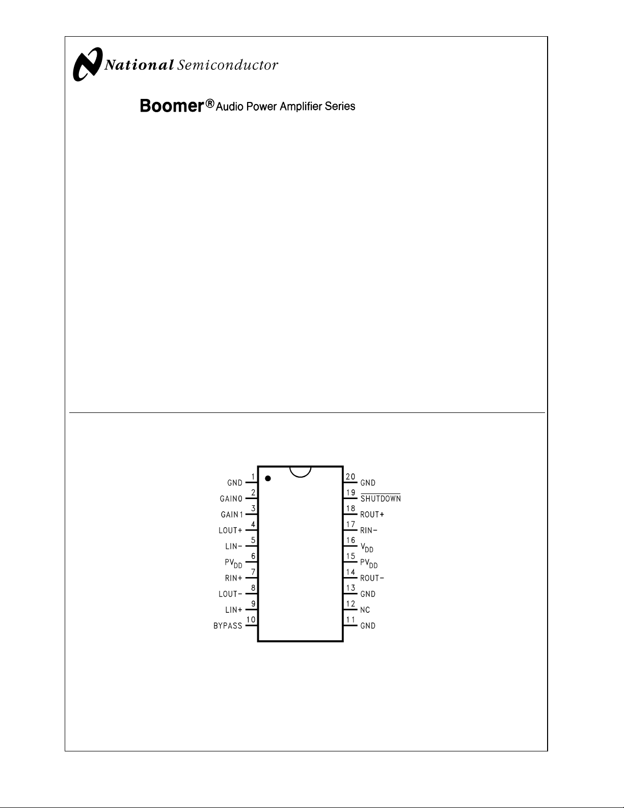
Connection Diagram
Top View
j
BTL output power
R
=8Ω,VDD= 5.0V, and THD+N = 1% 1.2W (typ)
L
j
Micropower shutdown current 0.1µA (typ)
j
PSRR (@1kHz, VDD= 5V, (Fig.1)) 62dB (typ)
Features
n Fully differential input and output
n Internal gain set: 6dB, 10dB, 15.6dB, and 21.6dB
n Improved ’click and pop’ suppression
n Thermal shutdown protection circuit
n Ultra low current micropower shutdown mode
n 3.0V to 5.5V operation
n Available in space-saving exposed-DAP TSSOP
package
Applications
n Notebook computers
n PDAs
n Portable electronic devices
Order Number LM4874MH
See NS Package Number MXA20A for Exposed-DAP TSSOP
Boomer®is a registered trademark of National Semiconductor Corporation.
© 2002 National Semiconductor Corporation DS200469 www.national.com
20046902
Page 2
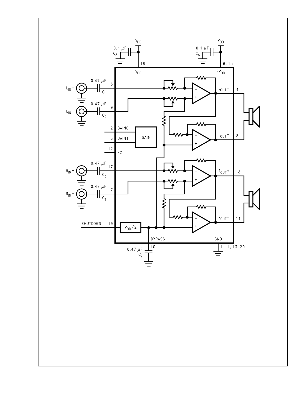
Typical Application
LM4874
FIGURE 1. Typical Audio Amplifier Application Circuit
www.national.com 2
20046901
Page 3
LM4874
Absolute Maximum Ratings (Notes 2,
3)
If Military/Aerospace specified devices are required,
please contact the National Semiconductor Sales Office/
Distributors for availability and specifications.
Supply Voltage 6.0V
Storage Temperature -65˚C to + 150˚C
Input Voltage −0.3V to V
Power Dissipation (Note 4) Internally Limited
ESD Susceptibility (Note 5) 2000V
ESD Susceptibility (Note 6) 200V
Junction Temperature 150˚C
Soldering Information
DD
+ 0.3V
Infrared (15 sec.) 220˚C
See AN-450 “Surface Mounting and their Effects on
Product Reliability” for other methods of soldering surface
mount devices.
Thermal Resistance
θ
(typ) MXA20A 2˚C/W
JC
θ
(typ) MXA20A 41˚C/W (Note 7)
JA
Operating Ratings
Temperature Range
≤ TA≤T
T
MIN
MAX
Supply Voltage 3.0 V ≤ V
−40˚C ≤ TA ≤ 85˚C
≤ 5.5V
DD
Small Outline Package
Vapor Phase (60 sec.) 215˚C
Electrical Characteristics for LM4874 (Notes 2, 8)
The following specifications applies to the LM4874 when used in the circuit shown in Figure 1 and operating with VDD=5Vand
= 6dB, unless otherwise specified. Limits apply for TA= 25˚C.
A
V
LM4874
Symbol Parameter Conditions
V
DD
Supply Voltage 3.0
Typical
(Note 8)
Limit
(Notes 9,
10)
5.5
I
DD
I
SD
V
OS
Quiescent Power Supply Current VIN= 0V, IO= 0A, RL=
Shutdown Current V
Output Offset Voltage 7 50 mV (max)
PSRR Output Supply Rejection Ratio V
P
O
Output Power (Note 11) THD+N = 1% (max), f = 1kHz (Note12)
shutdown
DD
= GND 0.1 1.0 µA (max)
= 5V, V
sinewave, C
=8Ω
R
L
=3Ω
R
L
=4Ω
R
L
=8Ω
R
L
RIPPLE
BYPASS
∞
= 200mV
= 0.47µF,
P-P
9.0 12.0 mA (max)
62 dB
2.1
1.9
1.2 1.0
THD+N = 10% (max), f = 1kHz
(Note12)
=3Ω
R
L
=4Ω
R
L
=8Ω
R
L
2.6
2.6
1.5
THD+N Total Harmonic Distortion + Noise 20Hz ≤ f ≤ 20kHz
=4Ω,PO=2W
R
L
=8Ω,PO=1W
R
L
S/N Signal-to-Noise Ratio f = 1kHz, C
= 1.1W, RL=8Ω
P
O
R
IN
Note 1: An LM4874MH that has been properly mounted to a circuit board with a copper heatsink area of at least 2in2will deliver 1.9W into 4Ω or 2.1W into 3Ω.
Note 2: All voltages are measured with respect to the GND pin unless other wise specified.
Note 3: Absolute Maximum Ratings indicate limits beyond which damage to the device may occur. Operating Ratings indicate conditions for which the device is
functional but do not guarantee specific performance limits. Electrical Characteristics state DC and AC electrical specifications under particular test conditions that
guarantee specific performance limits. This assumes that the device is within the Operating Ratings. Specifications are not guaranteed for parameters where no limit
is given, however, the typical value is a good indication of device performance.
Note 4: The maximum power dissipation must be derated at elevated temperatures and is dictated by TJMAX, θ
allowable power dissipation is P
currents for more information.
Note 5: Human body model, 100 pF discharged through a 1.5 kΩ resistor.
Input Resistance Pins 5, 7, 9, and 17 See Table 1.
DMAX
=(T
JMAX-TA/θJA
or the number given in Absolute Maximum Ratings, whichever is lower. For the LM4874, see power derating
BYPASS
= 0.47µF,
JA
0.3
0.3
97 dB
, and the ambient temperature, TA. The maximum
Units
(Limits)
V (min)
V (max)
W
W
W (min)
W
W
W
%
%
www.national.com3
Page 4
Electrical Characteristics for LM4874 (Notes 2, 8) (Continued)
Note 6: Machine Model, 220pF-240pF discharged through all pins.
LM4874
Note 7: The given θ
driving 4Ω loads from a 5V supply, the LM4874MH must be mounted to the circuit board and its exposed-DAP soldered to an exposed 2in
Note 8: Typicals are measured at 25˚C and represent the parametric norm.
Note 9: Limits are guaranteed to National’s AOQL (Average Outgoing Quality Level).
Note 10: Datasheet minimum and maximum specification limits are guaranteed by design, test, or statistical analysis.
Note 11: Output power is measured at the amplifier’s package pins.
Note 12: When driving 3Ω or 4Ω loads and operating on a 5V supply, the LM4874MH must be mounted to a circuit board that has a minimum of 2in
uninterrupted copper area connected to the MH package’s exposed DAP.
is for an LM4874 packaged in an MXA20A with the exposed-DAP soldered to an exposed 2in2area of 1oz printed circuit board copper. When
JA
External Components Description
See Figure 1.
Components Functional Description
1. C
2. C
The input coupling capacitor blocks DC voltage at the amplifier’s inverting input terminals. Ci, along with the
i
LM4874’s variable input resistance R
inverting and noninverting inputs require a C
EXTERNAL COMPONENTS, for an explanation of determining the value of C
The supply bypass capacitor. Refer to the POWER SUPPLY BYPASSING section for information about
S
(See Table 1), creates a highpass filter with fC= 1/(2πRiCi). Both
1
. Refer to the Application Information section, SELECTING
i
.
i
properly placing, and selecting the value of, this capacitor.
3. C
The capacitor, CB, filters the half-supply voltage present on the BYPASS pin. Refer to the Application
B
Information section, SELECTING EXTERNAL COMPONENTS, for information concerning proper placement
and selecting C
’s value.
B
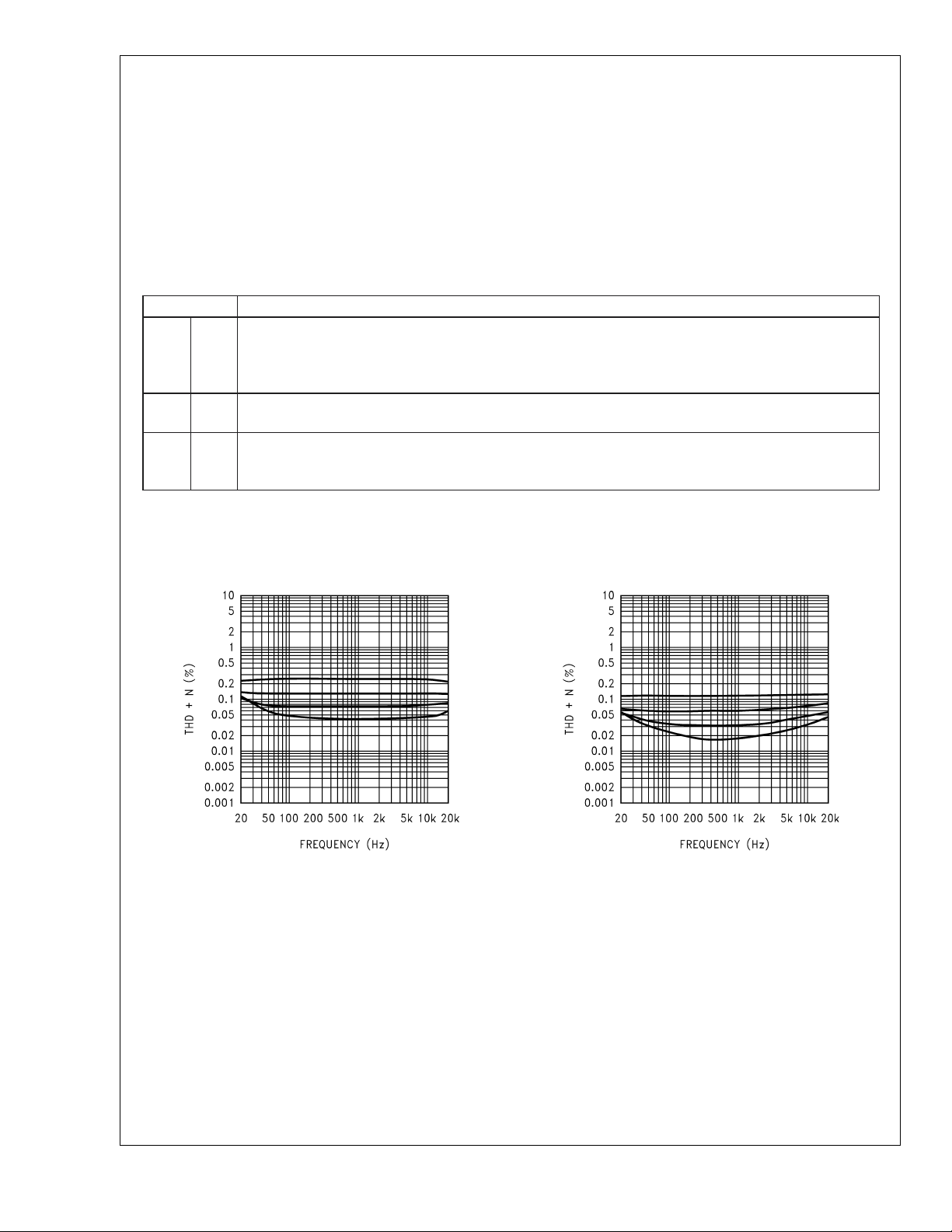
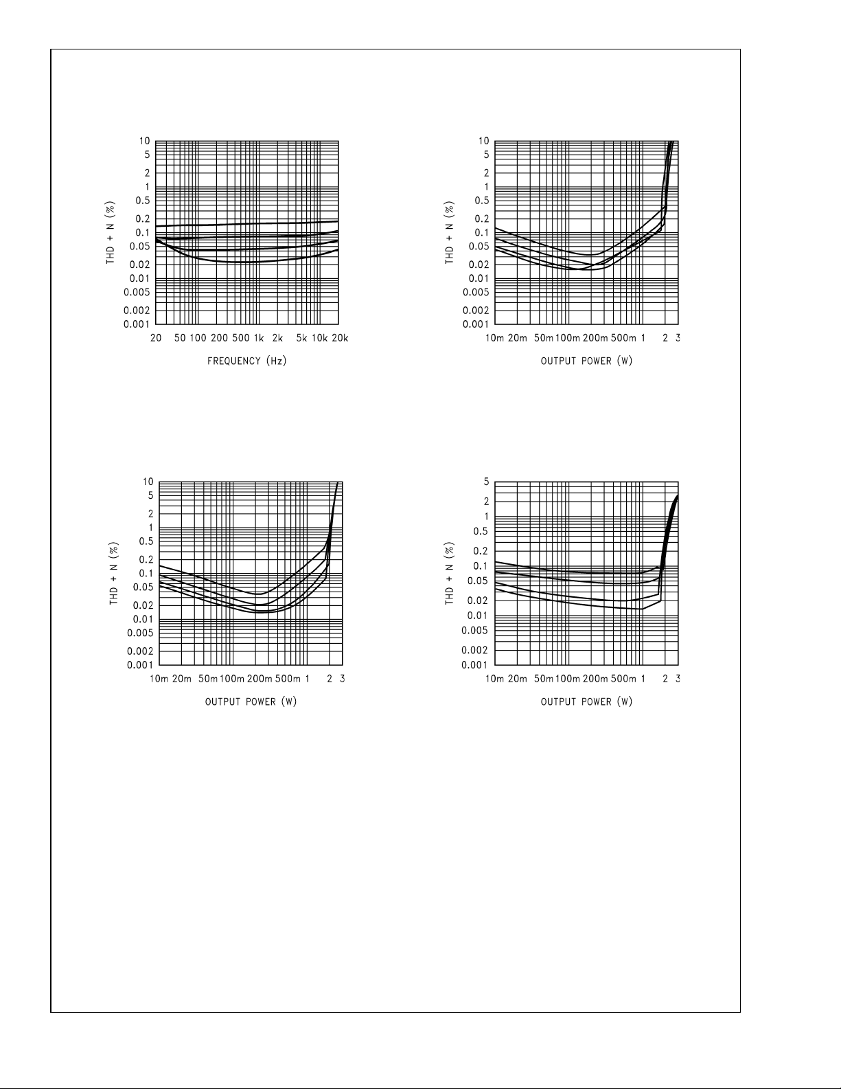
Typical Performance Characteristics MH Specific Characteristics
2
area of 1oz PCB copper.
2
of exposed,
THD vs Frequency THD vs Frequency
VDD= 5V, RL=4Ω,P
= 1000mW,
OUT
at (from top to bottom at 1kHz):
= 21.6dB, AV= 15.6dB,
A
V
= 10dB, AV= 6dB
A
V
20046998
VDD= 5V, RL=8Ω,P
OUT
= 400mW,
at (from top to bottom at 1kHz):
= 21.6dB, AV= 15.6dB,
A
V
= 10dB, AV= 6dB
A
V
20046997
www.national.com 4
Page 5
Typical Performance Characteristics
MH Specific Characteristics
THD vs Frequency THD vs Frequency
(Continued)
LM4874
VDD= 5V, RL=8Ω,P
OUT
= 400mW,
at (from top to bottom at 1kHz):
= 21.6dB, AV= 15.6dB,
A
V
= 10dB, AV= 6dB
A
V
THD vs Frequency THD vs Frequency
VDD= 5V, RL=3Ω,fIN= 1kHz,
at (from top to bottom at 50mW):
= 21.6dB, AV= 15.6dB,
A
V
= 10dB, AV= 6dB
A
V
20046999
20046944
VDD= 5V, RL=3Ω,fIN= 20Hz,
at (from top to bottom at 50mW):
= 21.6dB, AV= 15.6dB,
A
V
= 10dB, AV= 6dB
A
V
VDD= 5V, RL=3Ω,fIN= 20kHz,
at (from top to bottom at 50mW):
= 21.6dB, AV= 15.6dB,
A
V
= 10dB, AV= 6dB
A
V
20046943
20046945
www.national.com5
Page 6
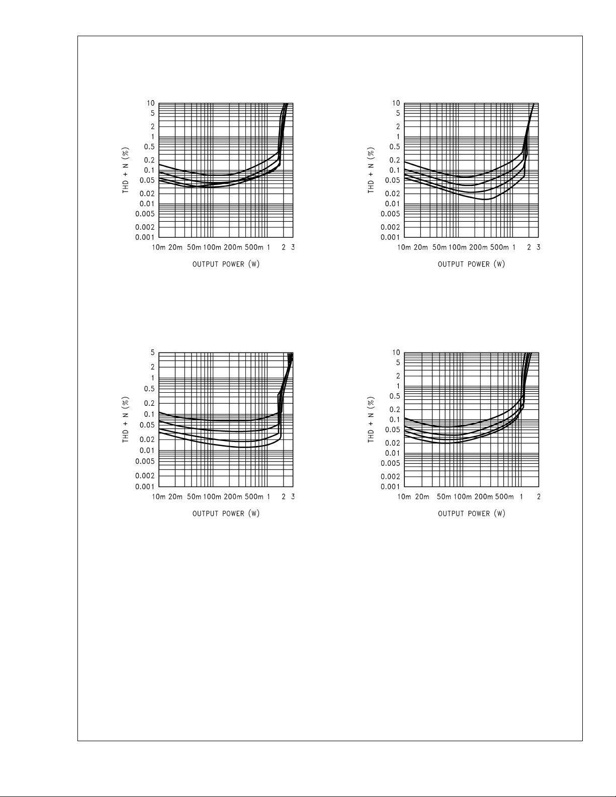
Typical Performance Characteristics
MH Specific Characteristics
LM4874
THD vs Output Power THD vs Output Power
(Continued)
VDD= 5V, RL=4Ω,fIN= 20Hz,
at (from top to bottom at 100mW):
= 21.6dB, AV= 15.6dB,
A
V
= 6dB, AV= 10dB
A
V
200469A0
VDD= 5V, RL=4Ω,fIN= 1kHz,
at (from top to bottom at 200mW):
= 21.6dB, AV= 15.6dB,
A
V
= 10dB, AV= 6dB
A
V
THD vs Output Power THD vs Output Power
VDD= 5V, RL=4Ω,fIN= 20kHz,
at (from top to bottom at 200mW):
= 21.6dB, AV= 15.6dB,
A
V
= 10dB, AV= 6dB
A
V
200469A2
VDD= 5V, RL=8Ω,fIN= 20Hz,
at (from top to bottom at 200mW):
= 21.6dB, AV= 15.6dB,
A
V
= 10dB, AV= 6dB
A
V
200469A1
200469A3
www.national.com 6
Page 7
Typical Performance Characteristics
MH Specific Characteristics
THD vs Output Power THD vs Output Power
(Continued)
LM4874
VDD= 5V, RL=8Ω,fIN= 1kHz,
at (from top to bottom at 200mW):
= 21.6dB, AV= 15.6dB,
A
V
= 10dB, AV= 6dB
A
V
200469A4
VDD= 5V, RL=8Ω,fIN= 20kHz,
at (from top to bottom at 200mW):
= 21.6dB, AV= 15.6dB,
A
V
= 10dB, AV= 6dB
A
V
Output Power vs Supply Voltage Output Power vs Supply Voltage
RL=4Ω,fIN= 1kHz,
at (from top to bottom at 4V):
THD+N = 10%, THD+N = 1%
200469C3
RL=8Ω,fIN= 1kHz,
at (from top to bottom at 4V):
THD+N = 10%, THD+N = 1%
200469A5
200469C4
www.national.com7
Page 8

Typical Performance Characteristics
MH Specific Characteristics
LM4874
PSRR vs Frequency PSRR vs Frequency
(Continued)
V
RIPPLE
VDD= 5V, RL=4Ω,R
= 200mV
, at (from top to bottom at 1kHz):
P-P
= 21.6dB, AV= 15.6dB,
A
V
= 10dB, AV= 6dB
A
V
SOURCE
THD vs Frequency THD vs Frequency
VDD= 3V, RL=4Ω,P
OUT
= 150mW,
at (from top to bottom at 1kHz):
= 21.6dB, AV= 15.6dB,
A
V
= 10dB, AV= 6dB
A
V
=10Ω
200469A8
200469B0
V
RIPPLE
VDD= 5V, RL=8Ω,R
= 200mV
, at (from top to bottom at 1kHz):
P-P
= 21.6dB, AV= 15.6dB,
A
V
= 10dB, AV= 6dB
A
V
VDD= 3V, RL=8Ω,P
SOURCE
OUT
= 150mW,
at (from top to bottom at 1kHz):
= 21.6dB, AV= 15.6dB,
A
V
= 10dB, AV= 6dB
A
V
200469A9
=10Ω
200469B1
www.national.com 8
Page 9

Typical Performance Characteristics
MH Specific Characteristics
THD vs Output Power THD vs Output Power
(Continued)
LM4874
VDD= 3V, RL=4Ω,fIN= 1kHz,
at (from top to bottom at 200mW):
= 21.6dB, AV= 6dB,
A
V
= 15.6dB, AV= 10dB
A
V
200469B3
VDD= 3V, RL=4Ω,fIN= 20Hz,
at (from top to bottom at 100mW):
= 21.6dB, AV= 15.6dB,
A
V
= 6dB, AV= 10dB
A
V
THD vs Output Power THD vs Output Power
VDD= 3V, RL=4Ω,fIN= 20kHz,
at (from top to bottom at 200mW):
= 21.6dB, AV= 15.6dB,
A
V
= 10dB, AV= 6dB
A
V
200469B4
VDD= 3V, RL=8Ω,fIN= 20Hz,
at (from top to bottom at 100mW):
= 21.6dB, AV= 6dB,
A
V
= 15.6dB, AV= 10dB
A
V
200469B2
200469B5
www.national.com9
Page 10

Typical Performance Characteristics
MH Specific Characteristics
LM4874
THD vs Output Power THD vs Output Power
(Continued)
V
RIPPLE
VDD= 3V, RL=8Ω,fIN= 1kHz,
at (from top to bottom at 200mW):
= 21.6dB, AV= 15.6dB,
A
V
= 6dB, AV= 10dB
A
V
PSRR vs Frequency PSRR vs Frequency
VDD= 3V, RL=4Ω,R
= 200mV
, at (from top to bottom at 1kHz):
P-P
= 21.6dB, AV= 15.6dB,
A
V
= 10dB, AV= 6dB
A
V
SOURCE
=10Ω,
200469B6
200469B8
V
RIPPLE
VDD= 3V, RL=8Ω,fIN= 20kHz,
at (from top to bottom at 200mW):
= 21.6dB, AV= 15.6dB,
A
V
= 10dB, AV= 6dB
A
V
VDD= 3V, RL=8Ω,R
= 200mV
, at (from top to bottom at 1kHz):
P-P
= 21.6dB, AV= 15.6dB,
A
V
= 10dB, AV= 6dB
A
V
SOURCE
=10Ω,
200469B7
200469B9
www.national.com 10
Page 11

Typical Performance Characteristics
MH Specific Characteristics
(Continued)
LM4874
Output Power vs
Load Resistance
fIN= 1kHz, at (from top to bottom at 20Ω):
200469C0
= 5V, THD = 10%; VDD= 5V, THD = 1%;
V
DD
= 3V, THD = 10%; VDD= 3V, THD = 1%
V
DD
Channel-to-Channel gain Mismatch
vs Power Supply Voltage
Channel-to-Channel gain Mismatch
vs Power Supply Voltage
RL=4Ω,fIN= 1kHz,
at (from top to bottom at 4V):
= 21.6dB, AV= 15.6dB,
A
V
= 10dB, AV= 6dB
A
V
Dropout Voltage
vs Power Supply Voltage
200469C1
RL=8Ω,fIN= 1kHz,
at (from top to bottom at 4V):
= 21.6dB, AV= 15.6dB,
A
V
= 10dB, AV= 6dB
A
V
200469C2
RL=8Ω,fIN= 1kHz, both channels driven and loaded
200469C5
at (from top to bottom at 4V):
positive signal swing, negative signal swing
www.national.com11
Page 12

Typical Performance Characteristics
MH Specific Characteristics
LM4874
(Continued)
Dropout Voltage
vs Power Supply Voltage
200469C6
RL=4Ω,fIN= 1kHz, both channels driven and loaded
at (from top to bottom at 4V):
positive signal swing, negative signal swing
Amplifier Power Dissipation
vs Amplifier Load Dissipation Cross Talk vs Frequency
Amplifier Power Dissipation
vs Amplifier Load Dissipation
VDD= 5V, fIN= 1kHz, at (from top to bottom at 1W):
200469C7
=4Ω,RL=8Ω, single channel driven and loaded
R
L
VDD= 3V, fIN= 1kHz, at (from top to bottom at 0.3W):
200469C8
=4Ω,RL=8Ω, single channel driven and loaded
R
L
www.national.com 12
VDD= 5V, RL=8Ω,AV= 6dB,
200469C9
A = Left channel driven, right channel measured;
B = Right channel driven, left channel measured
Page 13

Typical Performance Characteristics
MH Specific Characteristics
Cross Talk vs Frequency Cross Talk vs Frequency
(Continued)
LM4874
VDD= 5V, RL=8Ω,AV= 10dB,
200469D0
A = Left channel driven, right channel measured;
B = Right channel driven, left channel measured
Cross Talk vs Frequency Cross Talk vs Frequency
200469D2
VDD= 5V, RL=8Ω,AV= 21.6dB,
A = Left channel driven, right channel measured;
B = Right channel driven, left channel measured
VDD= 5V, RL=8Ω,AV= 15.6dB,
200469D1
A = Left channel driven, right channel measured;
B = Right channel driven, left channel measured
200469D3
VDD= 3V, RL=8Ω,AV= 6dB,
A = Left channel driven, right channel measured;
B = Right channel driven, left channel measured
www.national.com13
Page 14

Typical Performance Characteristics
MH Specific Characteristics
LM4874
Cross Talk vs Frequency Cross Talk vs Frequency
(Continued)
VDD= 3V, RL=8Ω,AV= 10dB,
200469D4
A = Left channel driven, right channel measured;
B = Right channel driven, left channel measured
Cross Talk vs Frequency
VDD= 3V, RL=8Ω,AV= 21.6dB,
A = Left channel driven, right channel measured;
B = Right channel driven, left channel measured
VDD= 3V, RL=8Ω,AV= 15.6dB,
200469D5
A = Left channel driven, right channel measured;
B = Right channel driven, left channel measured
200469D6
www.national.com 14
Page 15

Application Information
PCB LAYOUT AND SUPPLY REGULATION CONSIDERATIONS FOR DRIVING 3W AND 4W LOADS
Power dissipated by a load is a function of the voltage swing
across the load and the load’s impedance. As load impedance decreases, load dissipation becomes increasingly dependent on the interconnect (PCB trace and wire) resistance
between the amplifier output pins and the load’s connections. Residual trace resistance causes a voltage drop,
which results in power dissipated in the trace and not in the
load as desired. For example, 0.1Ω trace resistance reduces
the output power dissipated by a 4Ω load from 2.1W to 2.0W.
This problem of decreased load dissipation is exacerbated
as load impedance decreases. Therefore, to maintain the
highest load dissipation and widest output voltage swing,
PCB traces that connect the output pins to a load must be as
wide as possible.
Poor power supply regulation also adversely affects maximum output power. A poorly regulated supply’s output voltage decreases with increasing load current. Reduced supply
voltage causes decreased headroom, output signal clipping,
and reduced output power. Even with tightly regulated supplies, trace resistance creates the same effects as poor
supply regulation. Therefore, making the power supply
traces as wide as possible helps maintain full output voltage
swing.
BRIDGE CONFIGURATION EXPLANATION
As shown in Figure 1, each of the LM4874’s stereo channels
consists of two operational amplifiers. The LM4874 can be
used to drive a speaker connected between the two outputs
of each channel’s amplifiers.
Figure 1 shows that the output of Amp1 serves as the input
to Amp2, which results in both amplifiers producing signals
identical in magnitude, but 180˚ out of phase. Taking advantage of this phase difference, a load is placed between
OUT+ and OUT- and driven differentially (commonly referred
to as ’bridge mode’). This results in a differential gain of
= 2(RF/RI) (1)
A
VD
Bridge mode is different from single-ended amplifiers that
drive loads connected between a single amplifier’s output
and ground. For a given supply voltage, bridge mode has a
distinct advantage over the single-ended configuration: its
differential output doubles the voltage swing across the load.
This results in four times the output power when compared
to a single-ended amplifier under the same conditions. This
increase in attainable output assumes that the amplifier is
not current limited or the output signal is not clipped. To
ensure minimum output signal clipping when selecting one
of the amplifier’s four closed-loop gains, refer to the Audio
Power Amplifier Design section.
Another advantage of the differential bridge output is no net
DC voltage across the load. This results from biasing OUT+
and OUT- at half-supply. This eliminates the coupling capacitor that single supply, single-ended amplifiers require. Eliminating an output coupling capacitor in a single-ended con-
figuration forces a single supply amplifier’s half-supply bias
voltage across the load. The current flow created by the
half-supply bias voltage increases internal IC power dissipation and may permanently damage loads such as speakers.
POWER DISSIPATION
Power dissipation is a major concern when designing a
successful bridged or single-ended amplifier. Equation (2)
states the maximum power dissipation point for a singleended amplifier operating at a given supply voltage and
driving a specified output load.
=(VDD)2/(2π2RL) Single-Ended (2)
P
DMAX
However, a direct consequence of the increased power delivered to the load by a bridge amplifier is an increase in the
internal power dissipation point for a bridge amplifier operating at the same given conditions.
=4*(VDD)2/(2π2RL) Bridge Mode (3)
P
DMAX
The LM4874 has four operational amplifiers in one package
and the maximum internal power dissipation is four times
that of a single-ended amplifier. From Equation (3), assuming a 5V power supply and an 8Ω load, the maximum power
dissipation point is 2W. The maximum power dissipation
point obtained from Equation (3) must not exceed the power
dissipation predicted by Equation (4):
P
DMAX
=(T
JMAX−TA
)/θ
JA
(4)
For the exposed DAP TSSOP package, θJA= 41˚C/W.
T
perature T
= 150˚C for the LM4874. For a given ambient tem-
JAMAX
, Equation (4) can be used to find the maximum
A
internal power dissipation supported by the IC packaging. If
the result of Equation (3) is greater than that of Equation (4),
decrease the supply voltage, increase the load impedance,
or reduce the ambient temperature. For a typical application
with a 5V power supply and an 8Ω load, the maximum
ambient temperature that does not violate the maximum
junction temperature is approximately 68˚C. This further assumes that a device is a surface mount part operating
around the maximum power dissipation point. Since internal
power dissipation is a function of output power, higher ambient temperatures are allowed as output power decreases.
Refer to the Typical Performance Characteristics curves for
power dissipation information at lower output power levels.
BTL GAIN SELECTION
The LM4874 features four fixed, internally set, BTL voltage
gains: 6dB, 10dB, 15.6dB, and 21.6dB. Select one of the
four gains by applying a logic level signal to the GAIN0
(MSB) and GAIN1 (LSB) digital inputs.
The closed-loop gain of the first amplifier is adjustable, having four different gains, whereas two internal 20kΩ resistors
set the second amplifier’s gain at -1. Table 1 below, shows
the state of the two logic inputs required to select one of the
four gain values.
LM4874
www.national.com15
Page 16

Application Information (Continued)
LM4874
Table 1. Gain Settings and Input Resistance
GAIN 0 GAIN 1 Selected Gain
Input Resistance
(dB)
0 0 6 90kΩ
0 1 10 70kΩ
1 0 15.6 45kΩ
1 1 21.6 25kΩ
POWER SUPPLY BYPASSING
As with any power amplifier, proper supply bypassing is
critical for low noise performance and high power supply
rejection. The capacitors connected to the bypass and power
supply pins should be placed as close to the LM4874 as
possible. The capacitor connected between the bypass pin
and ground improves the internal bias voltage’s stability,
producing improved PSRR. The improvements to PSRR
increase as the bypass pin capacitor value increases.
Typical applications employ a 5V regulator with 10µF and a
0.1µF filter capacitors that aid in supply stability. Their presence, however, does not eliminate the need for bypassing
the LM4874’s supply pins. The selection of bypass capacitor
values, especially C
, depends on desired PSRR require-
B
ments, click and pop performance (as explained in theSe-
lecting External Components section), system cost, and
size constraints.
MICRO-POWER SHUTDOWN
The LM4874 features an active-low micro-power shutdown
mode. The voltage applied to the SHUTDOWN pin controls
the LM4874’s shutdown function. Activate micro-power shutdown by applying 0V to the SHUTDOWN pin. The logic
threshold is typically 0.4V for a logic low and 1.5V for a logic
high. When active, the LM4874’s micro-power shutdown
feature turns off the amplifier’s bias circuitry, disables the
internal V
/2 generator, and forces the amplifier outputs
DD
into a high impedance state. The result is greatly reduced
power supply current. The low 0.1µA typical shutdown current is achieved by applying a voltage to the SHUTDOWN
pin that is as near to GND as possible. A voltage that is
greater than GND may increase the shutdown current.
There are a few methods to control the micro-power shutdown. These include using a single-pole, single-throw switch
(SPST), a microprocessor, or a microcontroller. When using
a switch, connect a 100kΩ pull-down resistor between the
SHUTDOWN pin and GND and the SPST switch between
the SHUTDOWN pin and V
. Select normal amplifier op-
DD
eration by closing the switch. Opening the switch applies
GND to the SHUTDOWN pin, activating micro-power shutdown. The switch and resistor guarantee that the SHUTDOWN pin will not float. This prevents unwanted state
changes. In a system with a microprocessor or a microcontroller, use a digital output to apply the active-state voltage to
the SHUTDOWN pin. Driving the SHUTDOWN pin with active circuitry eliminates the pull-down resistor.
(R
Table 2. Logic Level Truth Table for Shutdown Operation
SHUTDOWN OPERATIONAL
MODE
)
i
High Full Power, stereo
BTL amplifiers
Low Micro-power
Shutdown
SELECTING PROPER EXTERNAL COMPONENTS
Optimizing the LM4874’s performance requires properly selecting external components. Though the LM4874 operates
well when using external components with wide tolerances,
best performance is achieved by optimizing component values. The LM4874 is unity-gain stable, giving a designer
maximum design flexibility. The gain should be set to no
more than a given application requires. This allows the amplifier to achieve minimum THD+N and maximum signal-tonoise ratio. These parameters are compromised as the
closed-loop gain increases. However, low gain demands
input signals with greater voltage swings to achieve maximum output power. Fortunately, many signal sources such
as audio CODECs have outputs of 1V
RMS
(2.83V
P-P
).
Please refer to the Audio Power Amplifier Design section for
more information on selecting the proper gain.
Input Capacitor Value Selection
Amplifying the lowest audio frequencies requires high value
input coupling capacitors (C
and C3,C4) in Figure 1. A
I,C2
high value capacitor can be expensive and may compromise
space efficiency in portable designs. In many cases, however, the speakers used in portable systems, whether internal or external, have little ability to reproduce signals with
frequencies below 150Hz. Applications using speakers with
this limited frequency response reap little improvement by
using large input capacitor.
Besides effecting system cost and size, CI - C4 can also
affect on the LM4874’s turn-on and turn-off transient (’click
and pop’) performance. When the supply voltage is first
applied, a transient may be created as the charge on the
input capacitor changes from zero to a quiescent state. The
magnitude of the transient is proportional to the value of, and
more importantly, the mismatch between, the capacitors
connected to a given pair of inverting and non-inverting
inputs. The better the match, the less the transient magnitude.
Higher value capacitors need more time to reach a quiescent
DC voltage (usually V
/2) when charged with a fixed cur-
DD
rent. This fixed current is supplied through amplifiers input
pins. Thus, selecting an input capacitor value that is no
higher than necessary to meet the desired -3dB frequency
will reduce turn-on time and help ensure that transients are
minimized.
The LM4874’s nominal input resistance (R
minimum) and the input capacitor, C
)is25kΩ (20kΩ,
i
, form high pass filter
i
with a -3dB low frequency limit defined by equation (5).
www.national.com 16
= 1/2π(25kΩ)C
f
-3dB
i
(5)
As an example when using a speaker with a low frequency
limit of 150Hz, C
, is 0.047µF. The 0.47µF CIshown in Figure
I
1 allows the LM4874 to drive high efficiency, full range
speaker whose response extends below 30Hz.
Page 17

LM4874
Application Information (Continued)
Bypass Capacitor Value Selection
Besides optimizing the input capacitor value, careful consideration should be paid to value of C
nected between the BYPASS pin and ground. Since C
determines how fast the LM4874 settles to its quiescent
operating state, its value is critical when minimizing turn-on
transients. The slower the LM4874’s outputs ramp to their
quiescent DC voltage (nominally
turn-on transient. Choosing C
small value of C
(in the range of 0.047µF to 0.47µF), pro-
i
equal to 0.47µF along with a
B
duces a transient-free turn-on and shutdown function. As
discussed above, choosing C
no larger than necessary for
i
the desired bandwidth helps minimize turn-on transients.
OPTIMIZING OUTPUT TRANSIENT REDUCTION (CLICK AND POP PERFORMANCE)
The LM4874 contains circuitry to minimize turn-on and shutdown transients or ’clicks and pop’. For this discussion,
turn-on refers to either applying the power supply voltage or
when the shutdown mode is deactivated. While the power
supply voltage is ramping to its final value, the LM4874’s
internal amplifiers are configured as unity gain buffers. An
internal current source changes the voltage of the BYPASS
pin in a controlled, linear manner. Ideally, the amplifier inputs
and outputs track the voltage applied to the BYPASS pin.
The gain of the internal amplifiers remains unity until the
voltage on the bypass pin reaches 1/2 V
voltage on the BYPASS pin is stable, the device becomes
fully operational. Although the bypass pin current can not be
modified, changing the size of C
time and the magnitude of output transients. Increasing the
value of C
reduces the magnitude of turn-on transients.
B
However, this presents a tradeoff: as the size of C
creases, the turn-on time increases. There is a linear relationships between the size of C
time. The table shows some typical turn-on times for various
values of C
:
B
C
B
C
= 0.47µF Ci= 0.33µF
i
0.01µF 110ms 80ms
0.1µF 120ms 90ms
0.22µF 140ms 100ms
0.47µF 170ms 140ms
1.0µF 240ms 210ms
In order to eliminate ’clicks and pops’, all capacitors must be
discharged before turn-on. Rapidly switching V
allow the capacitors to fully discharge, which may cause
’clicks and pops’.
, the capacitor con-
B
1
⁄2VDD), the smaller the
. As soon as the
DD
alters the device’s turn-on
B
+ 2(CI) and the turn-on
B
To n
may not
DD
in-
B
The design begins by specifying the minimum supply voltage
necessary to obtain the desired output power. One way to
find the minimum supply voltage is to use the Output Power
vs Supply Voltage curve in the Typical Performance Char-
B
acteristics section. Another way, using Equation (6), is to
calculate the peak output voltage necessary to achieve the
desired output power for a given load impedance. To account for the amplifier’s dropout voltage, two additional voltages, based on the Dropout Voltage vs Supply Voltage in the
Typical Performance Characteristics curves, must be
added to the result obtained by Equation (6). The result is
Equation (7).
(6)
VDD≥ (V
OUTPEAK
+(V
OD
TOP
+V
OD
BOT
)) (7)
The Output Power vs Supply Voltage graph for an 8Ω load
indicates a minimum supply voltage of 4.6V. This is easily
met by the commonly used 5V supply voltage. The additional
voltage creates the benefit of headroom, allowing the
LM4874 to produce peak output power in excess of 1W
without clipping or other audible distortion. The choice of
supply voltage must also not create a situation that violates
of maximum power dissipation as explained above in the
Power Dissipation section.
After satisfying the LM4874’s power dissipation requirements, the minimum differential gain is found using Equation
(8).
(8)
Thus, a minimum gain of 2.83 allows the LM4874’s to reach
full output swing and maintain low noise and THD+N performance. For this example, let A
the gain will be set to 10dB (A
= 3. In the example design,
VD
= 3.2) by applying a logic
VD
low to GAIN 0 and a logic high to GAIN 1.
The last step in this design example is setting the amplifier’s
±
-3dB frequency bandwidth. To achieve the desired
0.25dB
pass band magnitude variation limit, the low frequency response must extend to at least one-fifth the lower bandwidth
limit and the high frequency response must extend to at least
five times the upper bandwidth limit. This extended bandwith
produces a gain variation of -0.17dB at the bandwith’s limits,
±
well within the
0.25dB desired limit. The results are an
AUDIO POWER AMPLIFIER DESIGN
Audio Amplifier Design: Driving 1W into an 8Ω Load
The following are the desired operational parameters:
Power Output: 1 W
Load Impedance: 8Ω
Input Level: 1 V
Input Impedance: 20 kΩ
Bandwidth: 100 Hz−20 kHz
±
0.25 dB
RMS
RMS
and an
= 100Hz/5 = 20Hz (9)
f
L
= 20kHz x 5 = 100kHz (10)
f
H
www.national.com17
Page 18

Application Information (Continued)
As mentioned in the External Components section, the inter-
LM4874
nal input resistor and C
amplifier’s lower bandpass frequency limit. Find the coupling
capacitor’s value using Equation (11).
The result is (using the minimum RINresistor value to ensure
correct magnitude response at 20Hz)
1/(2π
Use a 0.39µF capacitor, the closest standard value. The
product of the desired high frequency cutoff (100kHz in this
example) and the differential gain, A
per passband response limit. With A
100kHz, the closed-loop gain bandwidth product (GBWP) is
create a high pass filter that sets the
i
= 1/2π(20kΩ)C
f
-3dB
*
20kΩ*20Hz) = 0.398µF (12)
I
, determines the up-
VD
= 3.2 and fH=
VD
(11)
320kHz. This is less than the LM4874’s 3.5MHz GBWP. With
this margin, the amplifier can be used in designs that require
more differential gain while avoiding performance-restricting
bandwidth limitations.
Recommended Printed Circuit Board Layout
Figures 2 through 6 show the recommended four-layer PC
board layout that is optimized for the 20-pin MH-packaged
LM4874 and associated external components. This circuit is
designed for use with an external 5V supply and 3Ω (or
higher) speakers (or load resistors).
This circuit board is easy to use. Apply 5V and ground to the
board’s V
speakers (or load resistors) between the board’s -OUTA and
+OUTA and -OUTB and +OUTB pads. Apply balanced differential stereo input signals to the input pins labeled ’-INA,’
’+INA,’ ’-INB,’ and ’+INB.’
and GND terminals, respectively. Connect
DD
200469D7
FIGURE 2. Recommended MH PC Board Layout:
Component-Side Silkscreen
200469D8
FIGURE 3. Recommended MH PC Board Layout:
Component-Side Layout
www.national.com 18
Page 19

Recommended Printed Circuit Board Layout (Continued)
200469D9
FIGURE 4. Recommended MH PC Board Layout:
Upper Inner-Layer Layout
LM4874
200469E0
FIGURE 5. Recommended MH PC Board Layout:
Lower Inner-Layer Layout
200469E1
FIGURE 6. Recommended MH PC Board Layout:
Bottom-Side Layout
www.national.com19
Page 20

LM4874
www.national.com 20
Page 21

Physical Dimensions inches (millimeters) unless otherwise noted
LM4874 Boomer 2.1W Differential Input, BTL Output Stereo Audio Amplifier with Selectable Gain
and Shutdown
Exposed-DAP TSSOP Package
Order Number LM4874MH
NS Package Number MXA20A for Exposed-DAP TSSOP
LIFE SUPPORT POLICY
NATIONAL’S PRODUCTS ARE NOT AUTHORIZED FOR USE AS CRITICAL COMPONENTS IN LIFE SUPPORT
DEVICES OR SYSTEMS WITHOUT THE EXPRESS WRITTEN APPROVAL OF THE PRESIDENT AND GENERAL
COUNSEL OF NATIONAL SEMICONDUCTOR CORPORATION. As used herein:
1. Life support devices or systems are devices or
systems which, (a) are intended for surgical implant
into the body, or (b) support or sustain life, and
whose failure to perform when properly used in
accordance with instructions for use provided in the
2. A critical component is any component of a life
support device or system whose failure to perform
can be reasonably expected to cause the failure of
the life support device or system, or to affect its
safety or effectiveness.
labeling, can be reasonably expected to result in a
significant injury to the user.
National Semiconductor
Corporation
Americas
Email: support@nsc.com
www.national.com
National does not assume any responsibility for use of any circuitry described, no circuit patent licenses are implied and National reserves the right at any time without notice to change said circuitry and specifications.
National Semiconductor
Europe
Fax: +49 (0) 180-530 85 86
Email: europe.support@nsc.com
Deutsch Tel: +49 (0) 69 9508 6208
English Tel: +44 (0) 870 24 0 2171
Français Tel: +33 (0) 1 41 91 8790
National Semiconductor
Asia Pacific Customer
Response Group
Tel: 65-2544466
Fax: 65-2504466
Email: ap.support@nsc.com
National Semiconductor
Japan Ltd.
Tel: 81-3-5639-7560
Fax: 81-3-5639-7507
 Loading...