

Page 1
LM4871
3W Audio Power Amplifier with Shutdown Mode
General Description
The LM4871 is a mono bridged audio power amplifier capable of delivering 3W of continuous average power into a
3Ω load with less than 10% THD when powered by a 5V
power supply (Note 1). To conserve power in portable applications, the LM4871’s micropower shutdown mode (I
Q
=
0.6µA, typ) is activated when V
DD
is applied to the SHUT-
DOWN pin.
Boomer audio power amplifiers are designed specifically to
provide high power, high fidelity audio output. They require
few external components and operate on low supply voltages from 2.0V to 5.5V. Since the LM4871 does not require
output coupling capacitors, bootstrap capacitors, or snubber
networks, it is ideally suited for low-power portable systems
that require minimum volume and weight.
Additional LM4871 features include thermal shutdown protection, unity-gain stability, and external gain set.
Note 1: An LM4871LD that has been properlymountedtoa circuit board will
deliver 3W into 3Ω (at 10% THD). The other package options for the LM4871
will deliver 1.5W into 8Ω (at 10% THD). See the Application Information
sections for further information concerning the LM4871LD, LM4871MM,
LM4871M, and the LM4871N.
Key Specifications
n PO at 10% THD+N, 1kHz
n LM4871LD: 3Ω ,4Ωloads 3W (typ), 2.5W (typ)
n All other LM4871 packages: 8Ω load 1.5W (typ)
n Shutdown current 0.6µA (typ)
n Supply voltage range 2.0V to 5.5V
n THD at 1kHz at 1W continuous average output power
into 8Ω 0.5% (max)
Features
n No output coupling capacitors, bootstrap capacitors, or
snubber circuits required
n Unity-gain stable
n LLP, MSOP, SO, or DIP packaging
n External gain configuration capability
n Pin compatible with the LM4861
Applications
n Portable computers
n Desktop computers
n Low voltage audio systems
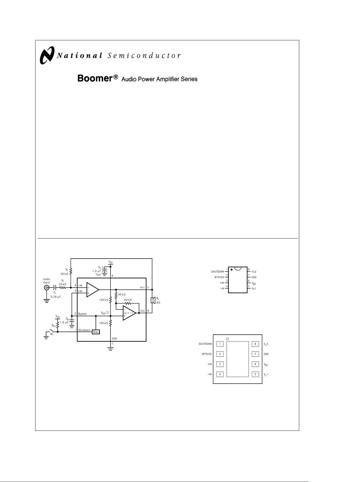
Typical Application Connection Diagram
Boomer®is a registered trademark of National Semiconductor Corporation.
DS100008-1
FIGURE 1. Typical Audio Amplifier Application Circuit
MSOP, Small Outline, and DIP Package
DS100008-2
Top View
Order Number LM4871MM, LM4871M, or LM4871N
See NS Package Number MUA08A, M08A, or N08E
LLP Package
DS100008-39
Top View
Order Number LM4871LD
See NS Package Number LDC08A
October 2000
LM4871 3W Audio Power Amplifier with Shutdown Mode
© 2000 National Semiconductor Corporation DS100008 www.national.com
Page 2
Absolute Maximum Ratings (Note 2)
If Military/Aerospace specified devices are required,
please contact the National Semiconductor Sales Office/
Distributors for availability and specifications.
Supply Voltage 6.0V
Supply Temperature −65˚C to +150˚C
Input Voltage −0.3V to V
DD
to +0.3V
Power Dissipation (Note 4) Internally Limited
ESD Susceptibility (Note 5) 5000V
ESD Susceptibility (Note 6) 250V
Junction Temperature 150˚C
Soldering Information
Small Outline Package
Vapor Phase (60 sec.) 215˚C
Infrared (15 sec.) 220˚C
See AN-450 ″Surface Mounting and their Effects on
Product Reliability″ for other methods of
soldering surface mount devices.
θ
JC
(typ)—M08A 35˚C/W
θ
JA
(typ)—M08A 140˚C/W
θ
JC
(typ)—N08E 37˚C/W
θ
JA
(typ)—N08E 107˚C/W
θ
JC
(typ)—MUA08A 56˚C/W
θ
JA
(typ)—MUA08A 210˚C/W
θ
JC
(typ)—LDC08A 4.3˚C/W
θ
JA
(typ)—LDC08A 56˚C/W (Note 9)
Operating Ratings
Temperature Range
T
MIN
≤ TA≤ T
MAX
−40˚C ≤ TA≤ 85˚C
Supply Voltage 2.0V ≤ V
DD
≤ 5.5V
Electrical Characteristics(Notes 2, 3)
The following specifications apply for V
DD
= 5V and RL=8Ωunless otherwise specified. Limits apply for TA= 25˚C.
Sym-
bol
Parameter Conditions
LM4871
Min
(Note 7)
Typical
(Note 8)
Limit
(Note 7)
Units
(Limits)
V
DD
Supply Voltage 2.0 5.5 V
I
DD
Quiescent Power Supply
Current
VIN= 0V, Io= 0A 6.5 10.0 mA
I
SD
Shutdown Current V
PIN1=VDD
0.6 2 µA
V
OS
Output Offset Voltage VIN= 0V 5.0 50 mV
P
o
Output Power THD = 1%, f = 1kHz
LM4871LD, R
L
=3Ω(Note 10)
LM4871LD, R
L
=4Ω(Note 10)
LM4871, R
L
=8Ω(Note 10)
2.38
2
1.2
W
THD+N = 10%, f = 1kHz
LM4871LD, R
L
=3Ω(Note 10)
LM4871LD, R
L
=4Ω(Note 10)
LM4871, R
L
=8Ω(Note 10)
3
2.5
1.5
W
THD+N Total Harmonic
Distortion+Noise
20Hz ≤ f ≤ 20kHz, A
VD
=2
LM4871LD, R
L
=4Ω,PO= 1.6W
LM4871, R
L
=8Ω,PO=1W
0.13
0.25
%
PSRR Power Supply Rejection
Ratio
V
DD
= 4.9V to 5.1V 60 dB
Note 2:
Absolute Maximum Ratings
indicate limits beyond which damage to the device may occur.
Operating Ratings
indicate conditions for which the device is
functional, but do not guarantee specific performance limits.
Electrical Characteristics
state DC and AC electrical specifications under particular test conditions which
guarantee specific performance limits. This assumes that the device is within the Operating Ratings. Specifications are not guaranteed for parameters where no limit
is given, however, the typical value is a good indication of device performance.
Note 3: All voltages are measured with respect to the ground pin, unless otherwise specified.
Note 4: The maximum power dissipation must be derated at elevated temperatures and is dictated by T
JMAX
, θJA, and the ambient temperature TA. The maximum
allowable power dissipation is P
DMAX
=(T
JMAX–TA
)/θJAor the number given in Absolute Maximum Ratings, whichever is lower. For the LM4871, T
JMAX
= 150˚C. For
the θ
JA
’s for different packages, please see the Application Information section or the Absolute Maximum Ratings section.
Note 5: Human body model, 100pF discharged through a 1.5kΩ resistor.
Note 6: Machine Model, 220pF–240pF discharged through all pins.
Note 7: Typicals are specified at 25˚C and represent the parametric norm.
Note 8: Limits are guaranteed to National’s AOQL (Average Outgoing Quality Level).
Note 9: The given θ
JA
is for an LM4871 packaged in an LDC08A with the Exposed–DAP soldered to an exposed 1in2area of 1oz printed circuit board copper.
Note 10: When driving 3Ω or 4Ω loads from a 5V supply, the LM4871LD must be mounted to a circuit board.
LM4871
www.national.com 2
Page 3
External Components Description (
Figure 1
)
Components Functional Description
1. R
i
Inverting input resistance that sets the closed-loop gain in conjunction with Rf. This resistor also forms a
high pass filter with C
i
at fC= 1/(2π RiCi).
2. C
i
Input coupling capacitor that blocks the DC voltage at the amplifiers input terminals. Also creates a highpass
filter with R
i
at fc= 1/(2π RiCi). Refer to the section, Proper Selection of External Components, for an
explanation of how to determine the value of C
i
.
3. R
f
Feedback resistance that sets the closed-loop gain in conjunction with Ri.
4. C
S
Supply bypass capacitor that provides power supply filtering. Refer to the Power Supply Bypassing section
for information concerning proper placement and selection of the supply bypass capacitor.
5. C
B
Bypass pin capacitor that provides half-supply filtering. Refer to the section, Proper Selection of External
Components, for information concerning proper placement and selection of C
B
.
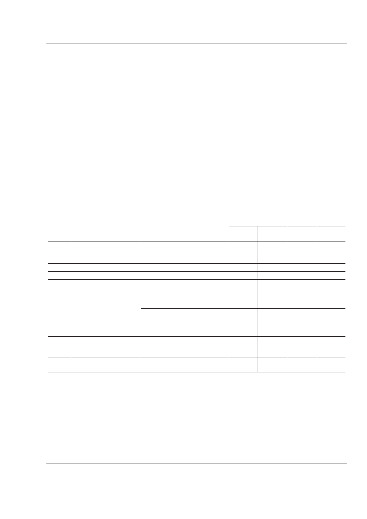
Typical Performance Characteristics
LD Specific Characteristics
Note 11: This curve shows the LM4871LD’s thermal dissipation ability at different ambient temperatures given the exposed-DAP of the part is soldered to a plane
of 1oz. Cu with an area given in the label of each curve. This label also designates whether the plane exists on the same (top) layer as the chip, on the bottom layer,
or on both layers. Infinite heatsink and unattached (no heatsink) conditions are also shown.
LM4871LD
THD+N vs Output Power
DS100008-24
LM4871LD
THD+N vs Frequency
DS100008-23
LM4871LD
THD+N vs Frequency
DS100008-25
LM4871LD
THD+N vs Output Power
DS100008-26
LM4871LD
Power Dissipation vs Output Power
DS100008-27
LM4871LD (Note 11)
Power Derating Curve
DS100008-28
LM4871
www.national.com3
Page 4
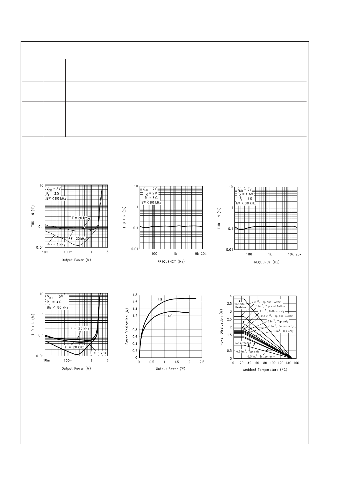
Typical Performance Characteristics
Non-LD Specific Characteristics
THD+N vs Frequency
DS100008-3
THD+N vs Frequency
DS100008-4
THD+N vs Frequency
DS100008-5
THD+N vs Output Power
DS100008-6
THD+N vs Output Power
DS100008-7
THD+N vs Output Power
DS100008-8
Output Power vs
Supply Voltage
DS100008-9
Output Power vs
Supply Voltage
DS100008-10
Output Power vs
Supply Voltage
DS100008-11
LM4871
www.national.com 4
Page 5

Typical Performance Characteristics
Non-LD Specific Characteristics
(Continued)
Output Power vs
Load Resistance
DS100008-12
Power Dissipation vs
Output Power
DS100008-13
Power Derating Curve
DS100008-14
Clipping Voltage vs
Supply Voltage
DS100008-15
Noise Floor
DS100008-16
Frequency Response vs
Input Capacitor Size
DS100008-17
Power Supply
Rejection Ratio
DS100008-18
Open Loop
Frequency Response
DS100008-19
Supply Current vs
Supply Voltage
DS100008-20
LM4871
www.national.com5
Page 6

Application Information
EXPOSED-DAP PACKAGE PCB MOUNTING
CONSIDERATION
The LM4871’s exposed-DAP (die attach paddle) package
(LD) provides a low thermal resistance between the die and
the PCB to which the part is mounted and soldered. This
allows rapid heat transfer from the die to the surrounding
PCB copper traces, ground plane, and surrounding air. The
result is a low voltage audio power amplifier that produces
2W at ≤ 1%THD with a 4Ω load.This high power is achieved
through careful consideration of necessary thermal design.
Failing to optimize thermal design may compromise the
LM4871’s high power performance and activate unwanted,
though necessary, thermal shutdown protection.
The LD package must have its DAP soldered to a copper
pad on the PCB.The DAP’sPCB copper pad is connected to
a large plane of continuous unbroken copper. This plane
forms a thermal mass, heat sink, and radiation area. Place
the heat sink area on either outside plane in the case of a
two-sided PCB, or on an inner layer of a board with more
than two layers. Connect the DAP copper pad to the inner
layer or backside copper heat sink area with 4(2x2) vias. The
via diameter should be 0.012in-0.013in with a 1.27mm pitch.
Ensure efficient thermal conductivity by plating through the
vias.
Best thermal performance is achieved with the largest practical heat sink area. If the heatsink and amplifier share the
same PCB layer, a nominal 2.5in
2
area is necessary for 5V
operation with a 4Ω load. Heatsink areas not placed on the
same PCB layer as the LM4871 should be 5in
2
(min) for the
same supply voltage and load resistance. The last two area
recommendations apply for 25˚C ambient temperature. Increase the area to compensate for ambient temperatures
above 25˚C. The LM4871’s power de-rating curve in the
TypicalPerformance Characteristics shows the maximum
power dissipation versus temperature. An example PCB layout for the LD package is shown in the Demonstration
Board Layout section. Further detailed and specific information concerning PCB layout, fabrication, and mounting an
LD (LLP) package is available from National Semiconductor’s Package Engineering Group under application note
AN1187.
PCB LAYOUT AND SUPPLY REGULATION
CONSIDERATIONS FOR DRIVING 3Ω AND 4Ω LOADS
Power dissipated by a load is a function of the voltage swing
across the load and the load’s impedance. As load impedance decreases, load dissipation becomes increasingly dependant on the interconnect (PCB trace and wire) resistance
between the amplifier output pins and the load’s connections. Residual trace resistance causes a voltage drop,
which results in power dissipated in the trace and not in the
load as desired. For example, 0.1Ω trace resistance reduces
the output power dissipated by a 4Ω load from 2.0W to
1.95W. This problem of decreased load dissipation is exacerbated as load impedance decreases. Therefore, to maintain the highest load dissipation and widest output voltage
swing, PCB traces that connect the output pins to a load
must be as wide as possible.
Poor power supply regulation adversely affects maximum
output power. A poorly regulated supply’s output voltage
decreases with increasing load current. Reduced supply
voltage causes decreased headroom, output signal clipping,
and reduced output power. Even with tightly regulated supplies, trace resistance creates the same effects as poor
supply regulation. Therefore, making the power supply
traces as wide as possible helps maintain full output voltage
swing.
BRIDGE CONFIGURATION EXPLANATION
As shown in
Figure 1
, the LM4871 has two operational
amplifiers internally, allowing for a few different amplifier
configurations. The first amplifier’s gain is externally configurable; the second amplifier is internally fixed in a unity-gain,
inverting configuration. The closed-loop gain of the first amplifier is set by selecting the ratio of R
f
to Riwhile the second
amplifier’s gain is fixed by the two internal 40kΩ resistors.
Figure 1
shows that the output of amplifier one serves as the
input to amplifier two, which results in both amplifiers producing signals identical in magnitude, but 180˚ out of phase.
Consequently, the differential gain for the IC is
A
VD
= 2 *(Rf/Ri)
By driving the load differentially through outputs Vo1 and
Vo2, an amplifier configuration commonly referred to as
“bridged mode” is established. Bridged mode operation is
different from the classical single-ended amplifier configuration where one side of its load is connected to ground.
A bridge amplifier design has a few distinct advantages over
the single-ended configuration, as it provides differential
drive to the load, thus doubling output swing for a specified
supply voltage. Four times the output power is possible as
compared to a single-ended amplifier under the same conditions. This increase in attainable output power assumes
that the amplifier is not current limited or clipped. In order to
choose an amplifier’s closed-loop gain without causing excessive clipping, please refer to the Audio Power Amplifier
Design section.
Another advantage of the differential bridge output is no net
DC voltage across load. This results from biasing V
O
1 and
V
O
2 at the same DC voltage, in this case VDD/2 . This
eliminates the coupling capacitor that single supply, singleended amplifiers require. Eliminating an output coupling capacitor in a single-ended configuration forces a single supply
amplifier’s half-supply bias voltage across the load. The
current flow created by the half-supply bias voltage increases internal IC power dissipation and my permanently
damage loads such as speakers.
POWER DISSIPATION
Power dissipation is a major concern when designing a
successful amplifier, whether the amplifier is bridged or
single-ended. A direct consequence of the increased power
delivered to the load by a bridge amplifier is an increase in
internal power dissipation. Equation 1 states the maximum
power dissipation point for a bridge amplifier operating at a
given supply voltage and driving a specified output load.
P
DMAX
= 4*(VDD)2/(2π2RL) (1)
Since the LM4871 has two operational amplifiers in one
package, the maximum internal power dissipation is 4 times
that of a single-ended ampifier. Even with this substantial
increase in power dissipation, the LM4871 does not require
heatsinking under most operating conditions and output
loading. From Equation 1, assuming a 5V power supply and
an 8Ω load, the maximum power dissipation point is
625 mW. The maximum power dissipation point obtained
from Equation 1 must not be greater than the power dissipation that results from Equation 2:
P
DMAX
=(T
JMAX–TA
)/θ
JA
(2)
For the SO package, θ
JA
= 140˚C/W, for the DIP package,
θ
JA
= 107˚C/W, and for the MSOP package, θJA= 210˚C/W
LM4871
www.national.com 6
Page 7

Application Information (Continued)
assuming free air operation. For the LD package soldered to
a DAP pad that expands to a copper area of 1.0in
2
on a
PCB, the LM4871’s θ
JA
is 56˚C/W. T
JMAX
= 150˚C for the
LM4871. The θ
JA
can be decreased by using some form of
heat sinking. The resultant θ
JA
will be the summation of the
θ
JC
, θCS, and θSA. θJCis the junction to case of the package
(or to the exposed DAP, as is the case with the LD package),
θ
CS
is the case to heat sink thermal resistance and θSAis the
heat sink to ambient thermal resistance. By adding additional copper area around the LM4871, the θ
JA
can be
reduced from its free air value for the SO and MSOP packages. Increasing the copper area around the LD package
from 1.0in
2
to 2.0in2area results in a θJAdecrease to
46˚C/W.Depending on the ambient temperature, T
A
, and the
θ
JA
, Equation 2 can be used to find the maximum internal
power dissipation supported by the IC packaging. If the
result of Equation 1 is greater than that of Equation 2, then
either the supply voltage must be decreased, the load impedance increased, the θ
JA
decreased, or the ambient temperature reduced. For the typical application of a 5V power
supply, with an 8Ω load, and no additional heatsinking, the
maximum ambient temperature possible withoutviolating the
maximum junction temperature is approximately 61˚C provided that device operation is around the maximum power
dissipation point and assuming surface mount packaging.
For the LD package in a typical application of a 5V power
supply, with a 4Ω load, and 1.0in
2
copper area soldered to
the exposed DAP pad, the maximum ambient temperature is
approximately 77˚C providing device operation is around the
maximum power dissipation point. Internal power dissipation
is a function of output power. If typical operation is not
around the maximum power dissipation point, the ambient
temperature can be increased. Refer to the Typical Perfor-
mance Characteristics curves for power dissipation information for different output powers and output loading.
POWER SUPPLY BYPASSING
As with any amplifier, proper supply bypassing is critical for
low noise performance and high power supply rejection. The
capacitor location on both the bypass and power supply pins
should be as close to the LM4871 as possible. The capacitor
connected between the bypass pin and ground improves the
internal bias voltage’s stability, producing improved PSRR.
The improvements to PSRR increase as the bypass pin
capacitor increases. Typical applications employ a 5V regulator with 10µF and a 0.1µF bypass capacitors which aid in
supply stability. This does not eliminate the need for bypassing the supply nodes of the LM4871 with a 1µF tantalum
capacitor.The selection of bypass capacitors, especially C
B
,
is dependent upon PSRR requirements, click and pop performance as explained in the section, Proper Selection of
External Components, system cost, and size constraints.
SHUTDOWN FUNCTION
In order to reduce power consumption while not in use, the
LM4871 contains a shutdown pin to externally turn off the
amplifier’s bias circuitry. This shutdown feature turns the
amplifier off when a logic high is placed on the shutdown pin.
The trigger point between a logic low and logic high level is
typically half- supply. It is best to switch between ground and
supply to provide maximum device performance. By switching the shutdown pin to V
DD
, the LM4871 supply current
draw will be minimized in idle mode. While the device will be
disabled with shutdown pin voltages less then V
DD
, the idle
current may be greater than the typical value of 0.6µA. In
either case, the shutdown pin should be tied to a definite
voltage to avoid unwanted state changes.
In many applications, a microcontroller or microprocessor
output is used to control the shutdown circuitry which provides a quick, smooth transition into shutdown. Another solution is to use a single-pole, single-throw switch in conjunction with an external pull-up resistor. When the switch is
closed, the shutdown pin is connected to ground and enables the amplifier. If the switch is open, then the external
pull-up resistor will disable the LM4871. This scheme guarantees that the shutdown pin will not float thus preventing
unwanted state changes.
PROPER SELECTION OF EXTERNAL COMPONENTS
Proper selection of external components in applications using integrated power amplifiers is critical to optimize device
and system performance. While the LM4871 is tolerant of
external component combinations, consideration to component values must be used to maximize overall system quality.
The LM4871 is unity-gain stable which gives a designer
maximum system flexibility. The LM4871 should be used in
low gain configurations to minimize THD+N values, and
maximize the signal to noise ratio. Low gain configurations
require large input signals to obtain a given output power.
Input signals equal to or greater than 1 Vrms are available
from sources such as audio codecs. Please refer to the
section, Audio Power Amplifier Design, for a more complete explanation of proper gain selection.
Besides gain, one of the major considerations is the closedloop bandwidth of the amplifier. To a large extent, the bandwidth is dictated by the choice of external components
shown in
Figure 1
. The input coupling capacitor, Ci, forms a
first order high pass filter which limits low frequency response. This value should be chosen based on needed
frequency response for a few distinct reasons.
Selection Of Input Capacitor Size
Large input capacitors are both expensive and space hungry
for portable designs. Clearly, a certain sized capacitor is
needed to couple in low frequencies without severe attenuation. But in many cases the speakers used in portable
systems, whether internal or external, have little ability to
reproduce signals below 100Hz to 150Hz. Thus, using a
large input capacitor may not increase actual system performance.
In addition to system cost and size, click and pop performance is effected by the size of the input coupling capacitor,
C
i.
A larger input coupling capacitor requires more charge to
reach its quiescent DC voltage (nominally 1/2 V
DD
). This
charge comes from the output via the feedback and is apt to
create pops upon device enable. Thus, by minimizing the
capacitor size based on necessary low frequency response,
turn-on pops can be minimized.
Besides minimizing the input capacitor size, careful consideration should be paid to the bypass capacitor value. Bypass
capacitor, C
B
, is the most critical component to minimize
turn-on pops since it determines how fast the LM4871 turns
on. The slower the LM4871’s outputs ramp to their quiescent
DC voltage (nominally 1/2 V
DD
), the smaller the turn-on pop.
Choosing C
B
equal to 1.0µF along with a small value of Ci(in
the range of 0.1µF to 0.39µF), should produce a virtually
clickless and popless shutdown function. While the device
will function properly, (no oscillations or motorboating), with
C
B
equal to 0.1µF, the device will be much more susceptible
LM4871
www.national.com7
Page 8

Application Information (Continued)
to turn-on clicks and pops. Thus, a value of C
B
equal to
1.0µF is recommended in all but the most cost sensitive
designs.
AUDIO POWER AMPLIFIER DESIGN
Design a 1W/8Ω Audio Amplifier
Given:
Power Output 1 Wrms
Load Impedance 8Ω
Input Level 1 Vrms
Input Impedance 20 kΩ
Bandwidth 100 Hz–20 kHz
±
0.25 dB
A designer must first determine the minimum supply rail to
obtain the specified output power. By extrapolating from the
Output Power vs Supply Voltage graphs in the Typical Per-
formance Characteristics section, the supply rail can be
easily found. A second way to determine the minimum supply rail is to calculate the required V
opeak
using Equation 3
and add the output voltage. Using this method, the minimum
supply voltage would be (V
opeak
+(V
OD
TOP
+V
OD
BOT
)), where
V
OD
BOT
and V
OD
TOP
are extrapolated from the Dropout Voltage vs Supply Voltage curve in the Typical Performance
Characteristics section.
(3)
Using the Output Power vs Supply Voltage graph for an 8Ω
load, the minimum supply rail is 4.6V. But since 5V is a
standard voltage in most applications, it is chosen for the
supply rail. Extra supply voltage creates headroom that allows the LM4871 to reproduce peaks in excess of 1W without producing audible distortion. At this time, the designer
must make sure that the power supply choice along with the
output impedance does not violate the conditions explained
in the Power Dissipation section.
Once the power dissipation equations have been addressed,
the required differential gain can be determined from Equation 4.
(4)
R
f/Ri=AVD
/2 (5)
From Equation 4, the minimum A
VD
is 2.83; use AVD=3.
Since the desired input impedance was 20kΩ, and with a
A
VD
impedance of 2, a ratio of 1.5:1 of Rfto Riresults in an
allocation of R
i
= 20kΩ and Rf= 30kΩ. The final design step
is to address the bandwidth requirements which must be
stated as a pair of −3dB frequency points. Five times away
from a −3dB point is 0.17dB down from passband response
which is better than the required
±
0.25dB specified.
f
L
= 100Hz/5 = 20Hz
f
H
= 20kHz*5=100kHz
As stated in the External Components section, R
i
in con-
junction with C
i
create a highpass filter.
C
i
≥ 1/(2π*20kΩ*20Hz) = 0.397µF; use 0.39µF
The high frequency pole is determined by the product of the
desired frequency pole, f
H
, and the differential gain, AVD.
With a A
VD
= 3 and fH= 100kHz, the resulting GBWP =
150kHz which is much smaller than the LM4871 GBWP of
4MHz. This figure displays that if a designer has a need to
design an amplifier with a higher differential gain, the
LM4871 can still be used without running into bandwidth
limitations.
LM4871
www.national.com 8
Page 9

Demonstration Board Layout
Recommended LD PC Board Layout:
Component-Side Silkscreen
DS100008-29
Recommended LD PC Board Layout:
Component-Side Layout
DS100008-30
Recommended LD PC Board Layout:
Bottom-Side Layout
DS100008-31
LM4871
www.national.com9
Page 10

Physical Dimensions inches (millimeters) unless otherwise noted
Order Number LM4871LD
See NS Package Number LDC08A
Order Number LM4871M
NS Package Number M08A
LM4871
www.national.com 10
Page 11

Physical Dimensions inches (millimeters) unless otherwise noted (Continued)
Order Number LM4871MM
NS Package Number MUA08A
LM4871
www.national.com11
Page 12

Physical Dimensions inches (millimeters) unless otherwise noted (Continued)
LIFE SUPPORT POLICY
NATIONAL’S PRODUCTS ARE NOT AUTHORIZED FOR USE AS CRITICAL COMPONENTS IN LIFE SUPPORT
DEVICES OR SYSTEMS WITHOUT THE EXPRESS WRITTEN APPROVAL OF THE PRESIDENT AND GENERAL
COUNSEL OF NATIONAL SEMICONDUCTOR CORPORATION. As used herein:
1. Life support devices or systems are devices or
systems which, (a) are intended for surgical implant
into the body, or (b) support or sustain life, and
whose failure to perform when properly used in
accordance with instructions for use provided in the
labeling, can be reasonably expected to result in a
significant injury to the user.
2. A critical component is any component of a life
support device or system whose failure to perform
can be reasonably expected to cause the failure of
the life support device or system, or to affect its
safety or effectiveness.
National Semiconductor
Corporation
Americas
Tel: 1-800-272-9959
Fax: 1-800-737-7018
Email: support@nsc.com
National Semiconductor
Europe
Fax: +49 (0) 180-530 85 86
Email: europe.support@nsc.com
Deutsch Tel: +49 (0) 69 9508 6208
English Tel: +44 (0) 870 24 0 2171
Français Tel: +33 (0) 1 41 91 8790
National Semiconductor
Asia Pacific Customer
Response Group
Tel: 65-2544466
Fax: 65-2504466
Email: ap.support@nsc.com
National Semiconductor
Japan Ltd.
Tel: 81-3-5639-7560
Fax: 81-3-5639-7507
www.national.com
Order Number LM4871N
NS Package Number N08E
LM4871 3W Audio Power Amplifier with Shutdown Mode
National does not assume any responsibility for use of any circuitry described, no circuit patent licenses are implied and National reserves the right at any time without notice to change said circuitry and specifications.
 Loading...