

Page 1
LM4870
1.1W Audio Power Amplifier with Shutdown Mode
LM4870 1.1W Audio Power Amplifier with Shutdown Mode
October 1997
General Description
The LM4870 is a bridge-connected audio power amplifier capable of delivering 1.1W of continuous average power to an
8Ω load with less than 0.5%THD+N over the audio spectrum
from a 5V power supply.
Boomer audio power amplifiers were designed specifically to
provide high quality output power with a minimal number of
external components. Since the LM4870 does not require
output coupling capacitors, bootstrap capacitors or snubber
networks, it is optimally suited for low-power portable systems.
The LM4870 features an externally controlled, low-power
consumption shutdown mode, as well as an internal thermal
shutdown protection mechanism. It also includes two headphone control inputs and a headphone sense output for external monitoring. The LM4870 is unity-gain stable and the
gain is set using external resistors.
Key Specifications
n THD+N at 1W into 8Ω 0.5%(max)
n Output power into 8Ω at 1kHz
at 10%THD+N
n Shutdown Current 0.6µA (typ)
Features
n No output coupling capacitors, bootstrap capacitors, or
snubber circuits are necessary
n Small Outline (SOIC) power packaging
n Unity-gain stable
n External gain configuration capability
Applications
n Personal computers
n Desktop computers
n Low voltage audio system
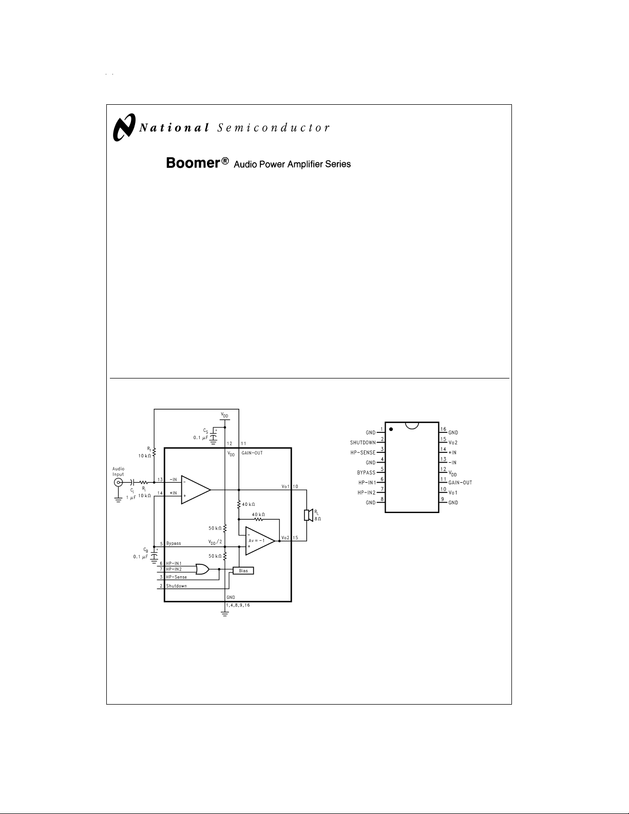
Typical Application Connection Diagram
Small Outline Package
1.5W (typ)
DS100094-2
Top View
Order Number LM4870M
See NS Package Number M16A
DS100094-1
FIGURE 1. Typical Audio Amplifier Application Circuit
Boomer®is a registered trademark of National Semiconductor Corporation.
© 1999 National Semiconductor Corporation DS100094 www.national.com
Page 2
Absolute Maximum Ratings (Note 2)
If Military/Aerospace specified devices are required,
please contact the National Semiconductor Sales Office/
Distributors for availability and specifications.
Supply Voltage 6.0V
Storage Temperature −65˚C to +150˚C
Input Voltage −0.3V to V
Power Dissipation Internally limited
ESD Susceptibility (Note 4) 3000V
ESD Susceptibility (Note 5) 250V
Junction Temperature 150˚C
Soldering Information
Small Outline Package
Vapor Phase (60 sec.) 215˚C
DD
+ 0.3V
Infrared (15 sec.) 220˚C
Thermal Resistance
(typ) 35˚C/W
φ
JC
(typ) 100˚C/W
φ
JA
See AN-450
“Surface Mounting and their Effects on Product
Reliability” for other methods of soldering surface mount devices.
Operating Ratings
Temperature Range
≤ TA≤ T
T
MIN
MAX
Supply Voltage 2.0V ≤ V
−20˚C ≤ TA≤ +85˚C
≤ 5.5V
DD
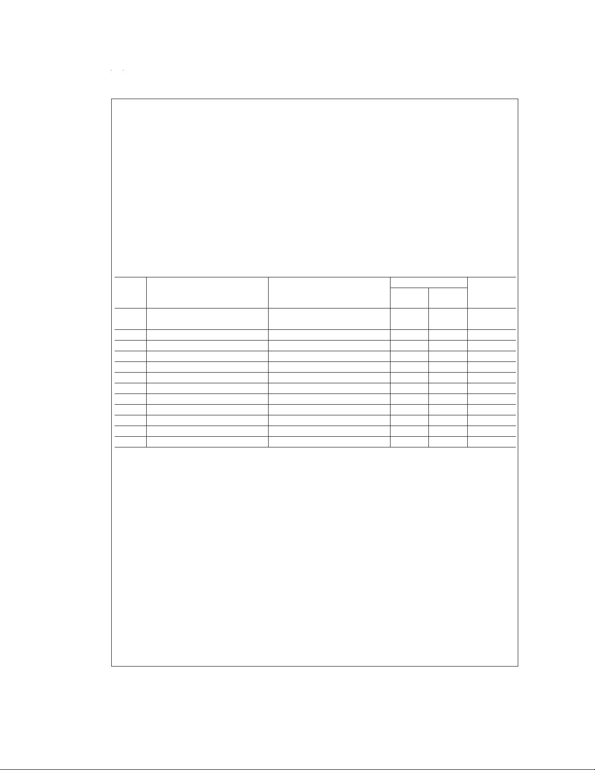
Electrical Characteristics
(Notes 1, 2) The following specifications apply for V
=
DD
Symbol Parameter Conditions LM4870 Units
V
I
DD
I
SD
V
P
THD+N Total Harmonic Distortion + Noise P
PSRR Power Supply Rejection Ratio V
V
V
V
V
V
Supply Voltage 2.0 V (min)
DD
Quiescent Power Supply Current V
Shutdown Current V
Output Offset Voltage V
OS
Output Power THD+N=0.5%(max); f=1 kHz 1.1 1.0 W (min)
O
Output Dropout Voltage V
od
HP-IN High Input Voltage HP-SENSE=0V to 4V 2.5 V
IH
HP-IN Low Input Voltage HP-SENSE=4V to 0V 2.5 V
IL
HP-SENSE High Output Voltage I
OH
HP-SENSE Low Output Voltage I
OL
Note 1: All voltages are measured with respect to the ground pins, unless otherwise specified.
Note 2: Absolute Maximum Ratings indicate limits beyond which damage to the device may occur. Operating Ratings indicate conditions for which the device is func-
tional, but do not guarantee specific performance limits. Electrical Characteristics state DC and AC electrical specifications under particular test conditions which guarantee specific performance limits. This assumes that the device is within the Operating Ratings. Specifications are not guaranteed for parameters where no limit is
given, however, the typical value is a good indication of device performance.
Note 3: The maximum power dissipation must be derated at elevated temperatures and is dictated by T
allowable power dissipation is P
+150˚C, and the typical junction-to-ambient thermal resistance, when board mounted, is 100˚C/W.
Note 4: Human body model, 100 pF discharged through a 1.5 kΩ resistor.
Note 5: Machine Model, 200 pF–240 pF discharged through all pins.
Note 6: Typicals are measured at 25˚C and represent the parametric norm.
Note 7: Limits are guaranteed to National’s AOQL (Average Outgoing Quality Level).
DMAX
=
(T
)/θJAor the number given in the Absolute Maximum Ratings, whichever is lower. For the LM4870, T
JMAX−TA
=
O
pin2
=
IN
=
O
=
DD
=
IN
=
500 µA 2.8 2.5 V (min)
O
=
−500 µA 0.2 0.8 V (max)
O
5V, R
=
8Ω unless otherwise specified. Limits apply for T
L
Typical Limit
=
A
(Limits)
25˚C.
(Note 6) (Note 7)
5.5 V (max)
=
0V, I
0A 7.0 15.0 mA (max)
O
=
V
DD
0.4 µA
0V 10 50.0 mV (max)
1 Wrms; 20 Hz ≤ f ≤ 20 kHz 0.25
%
4.9V to 5.1V 60 dB
0V to 5V 0.6 1.0 V (max)
, θJA, and the ambient temperature TA. The maximum
JMAX
JMAX
=
www.national.com 2
Page 3
External Components Description (
Figure 1
)
Components Functional Description
1. R
2. C
3. R
4. C
5. C
i
i
f
S
B
Inverting input resistance which sets the closed-loop gain in conjunction with Rf. This resistor also
forms a high pass filter with C
at f
1/(2π R
i
C
iCi
).
=
Input coupling capacitor which blocks DC voltage at the amplifier’s input terminals. Also creates a
highpass filter with R
at f
1/(2π R
i
C
iCi
).
=
Feedback resistance which sets closed-loop gain in conjunction with Ri.
Supply bypass capacitor which provides power supply filtering. Refer to the Application Information
section for proper placement and selection of supply bypass capacitor.
Bypass pin capacitor which provides half supply filtering. Refer to Application Information section for
proper placement and selection of bypass capacitor.
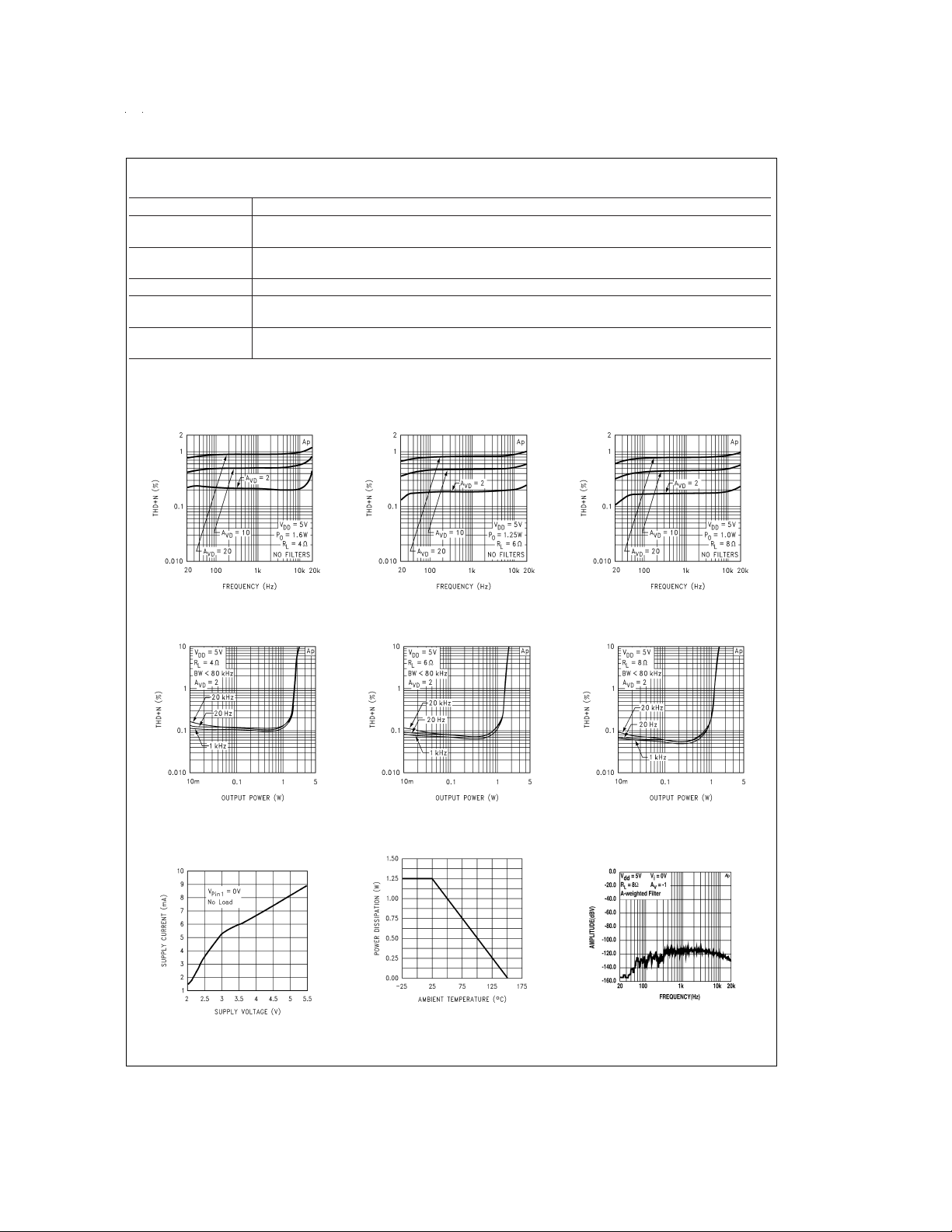
Typical Performance Characteristics
THD+N vs Frequency
THD+N vs Output Power
Supply Current vs
Supply Voltage
DS100094-9
DS100094-12
THD+N vs Frequency
THD+N vs Output Power
Power Derating Curve
DS100094-10
DS100094-13
THD+N vs Frequency
DS100094-11
THD+N vs Output Power
DS100094-14
LM4870 Noise Floor
vs Frequency
DS100094-16
DS100094-17
DS100094-18
www.national.com3
Page 4
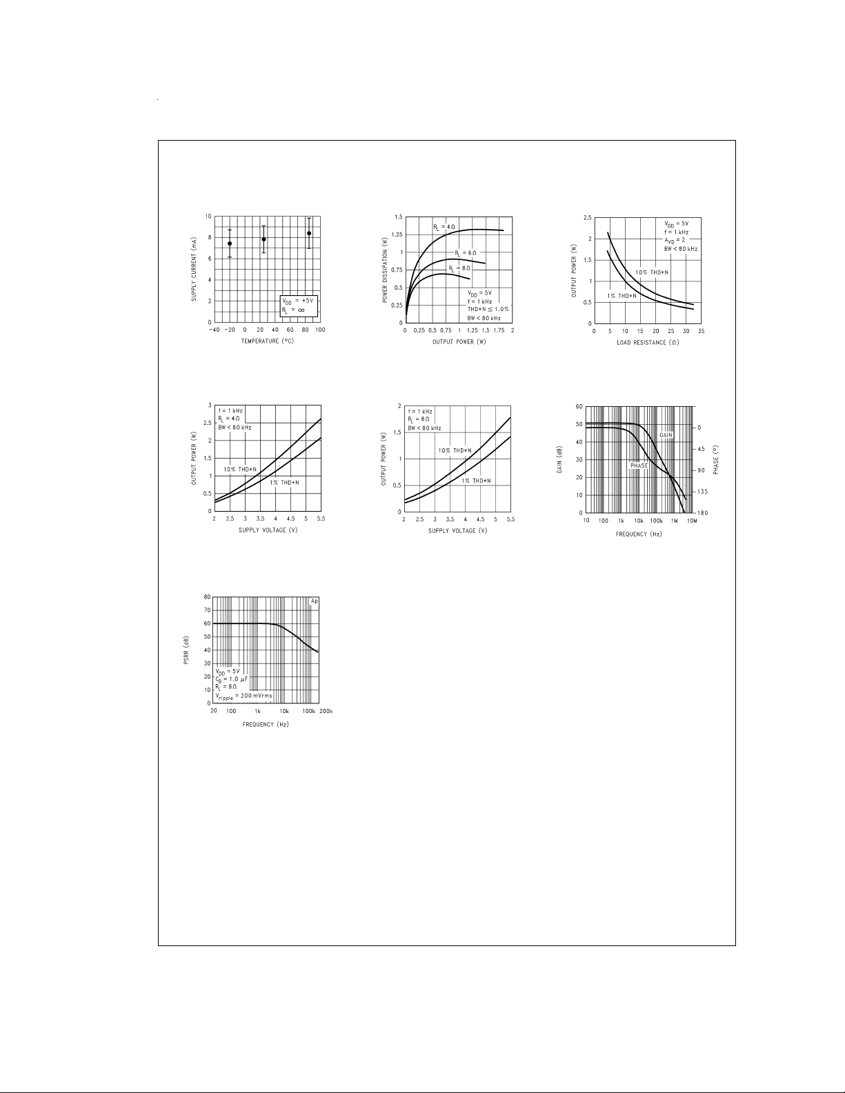
Typical Performance Characteristics (Continued)
Supply Current Distribution
vs Temperature
DS100094-19
Output Power vs
Supply Voltage
DS100094-22
Power Supply
Rejection Ratio
Power Dissipation
vs Output Power
Output Power vs
Supply Voltage
DS100094-20
DS100094-27
Output Power vs
Load Resistance
DS100094-21
Open Loop
Frequency Response
DS100094-23
DS100094-24
Application Information
BRIDGE CONFIGURATION EXPLANATION
Figure 1
As shown in
plifiers internally, allowing for a few different amplifier configurations. The first amplifier’s gain is externally configurable, while the second amplifier is internally fixed in a
unity-gain, inverting configuration. The closed-loop gain of
the first amplifier is set by selecting the ratio of R
the second amplifier’s gain is fixed by the two internal 40 kΩ
resistors.
Figure 1
serves as the input to amplifier two which results in both amplifiers producing signals identical in magnitude, but out of
phase 180˚. Consequently, the differential gain for the IC is:
www.national.com 4
, the LM4870 has two operational am-
to Riwhile
f
shows that the output of amplifier one
=
*
A
(Rf/Ri)
2
vd
By driving the load differentially through outputs V
V
, an amplifier configuration commonly referred to as
O2
“bridged mode” is established. Bridged mode operation is
and
O1
different from the classical single-ended amplifier configuration where one side of its load is connected to ground.
A bridge amplifier design has a few distinct advantages over
the single-ended configuration, as it provides differential
drive to the load, thus doubling output swing for a specified
supply voltage. Consequently, four times the output power is
possible as compared to a single-ended amplifier under the
same conditions. This increase in attainable output power
assumes that the amplifier is not current limited or clipped. In
order to choose an amplifier’s closed-loop gain without caus-
Page 5

Application Information (Continued)
ing excessive clipping which will damage high frequency
transducers used in loudspeaker systems, please refer to
the Audio Power Amplifier Deslgn section.
A bridge configuration, such as the one used in Boomer Audio Power Amplifiers, also creates a second advantage over
single-ended amplifiers. Since the differential outputs, V
and VO2, are biased at half-supply, no net DC voltage exists
across the load. This eliminates the need for an output coupling capacitor which is required in a single supply,
single-ended amplifier configuration. Without a large output
coupling capacitor in a single supply single-ended amplifier,
the half-supply bias across the load would result in both increased internal IC power dissipation.
POWER DISSIPATION
Power dissipation is a major concern when designing a successful amplifier, whether the amplifier is bridged or
single-ended. A direct consequence of the increased power
delivered to the load by a bridge amplifier is an increase in
internal power dissipation. Equation 1 states the maximum
power dissipation point for a bridge amplifier operating at a
given supply voltage and driving a specified output load.
Since the LM4870 has two operational amplifiers in one
package, the maximum internal power dissipation is 4 times
that of a single-ended amplifier. Even with this substantial increase in power dissipation, the LM4870 does not require
heatsinking. From Equation 1, assuming a 5V power supply
and an 8Ω load, the maximum power dissipation point is 625
mW. The maximum power dissipation point obtained from
Equation 1 must not be greater than the power dissipation
that results from Equation 2:
For the LM4870 surface mount package, θ
=
T
150˚C. Depending on the ambient temperature, T
JMAX
of the system surroundings, Equation 2 can be used to find
the maximum internal power dissipation supported by the IC
packaging. If the result of Equation 1 is greater than that of
Equation 2, then either the supply voltage must be decreased or the load impedance increased. For the typical application of a 5V power supply, with an 8Ω load, the maximum ambient temperature possible without violating the
maximum junction temperature is approximately 88˚C, provided that device operation is around the maximum power
dissipation point. Power dissipation is a function of output
power and thus, if typical operation is not around the maximum power dissipation point, the ambient temperature can
be increased. Refer to the TypicalPerformance Character-
istics curves for power dissipation information for lower output powers.
POWER SUPPLY BYPASSING
As with any power amplifier,proper supply bypassing is critical for low noise performance and high power supply rejection. The capacitor location on both the bypass and power
supply pins should be as close to the device as possible. As
displayed in the Typical Performance CharacterIstIcs section, the effect of a larger half-supply bypass capacitor is improved low frequency THD+N due to increased half-supply
stability. Typical applications employ a 5V regulator with
a10 µF tantalum and a 0.1 µF film bypass capacitors which
aid in supply stability, but do not eliminate the need for bypassing the supply nodes of the LM4870. The selection of
P
DMAX
P
DMAX
=
*
(VDD)2/(2π2RL)(1)
4
=
(T
JMAX−TA
)/θ
(2)
JA
=
100˚C/W and
JA
bypass capacitors, especially C
desired low frequency THD+N, system cost, and size con-
, is thus dependant upon
B
straints.
SHUTDOWN FUNCTION
In order to reduce power consumption while not in use, the
LM4870 contains a shutdown pin to externally turn off the
O1
amplifier’s bias circuitry. The shutdown feature turns the amplifier off when a logic high is placed on the shutdown pin.
Upon going into shutdown, the output is immediately disconnected from the speaker. There is a built-in threshold which
produces a drop in quiescent current to 500 µA typically. For
a 5V power supply, this threshold occurs when 2V–3V is applied to the shutdown pin. A typical quiescent current of
0.6 µA results when the supply voltage is applied to the shutdown pin. In many applications, a microcontroller or microprocessor output is used to control the shutdown circuitry
which provides a quick, smooth transition into shutdown. Another solution is to use a single-pole, single-throw switch that
when closed, is connected to ground and enables the amplifier.If the switch is open, then a soft pull-up resistor of 47 kΩ
will disable the LM4870. There are no soft pull-down resistors inside the LM4870, so a definite shutdown pin voltage
must be applied externally, or the internal logic gate will be
left floating which could disable the amplifier unexpectedly.
HEADPHONE CONTROL INPUTS
The LM4870 possesses two headphone control inputs that
disable the amplifier and reduce I
either one or both of these inputs have a logic-high voltage
to less than 1 mA when
DD
placed on their pins.
Unlike the shutdown function, the headphone control func-
tion does not provide the level of current conservation that is
required for battery powered systems. Since the quiescent
current resulting from the headphone control function is
1000 times more than the shutdown function, the residual
A
coming out of the headphone control mode. The pop effect
currents in the device may create a pop at the output when
,
may be eliminated by connecting the headphone sensing
output to the shutdown pin input as shown in
Figure 2
. This
solution will not only eliminate the output pop, but will also
utilize the full current conservation of the shutdown function
by reducing I
shutdown. This configuration also allows the designer to use
to 0.6 µA. The amplifier will then be fully
DD
the control inputs as either two headphone control pins or a
headphone control pin and a shutdown pin where the lowest
level of current consumption is obtained from either function.
Figure 3
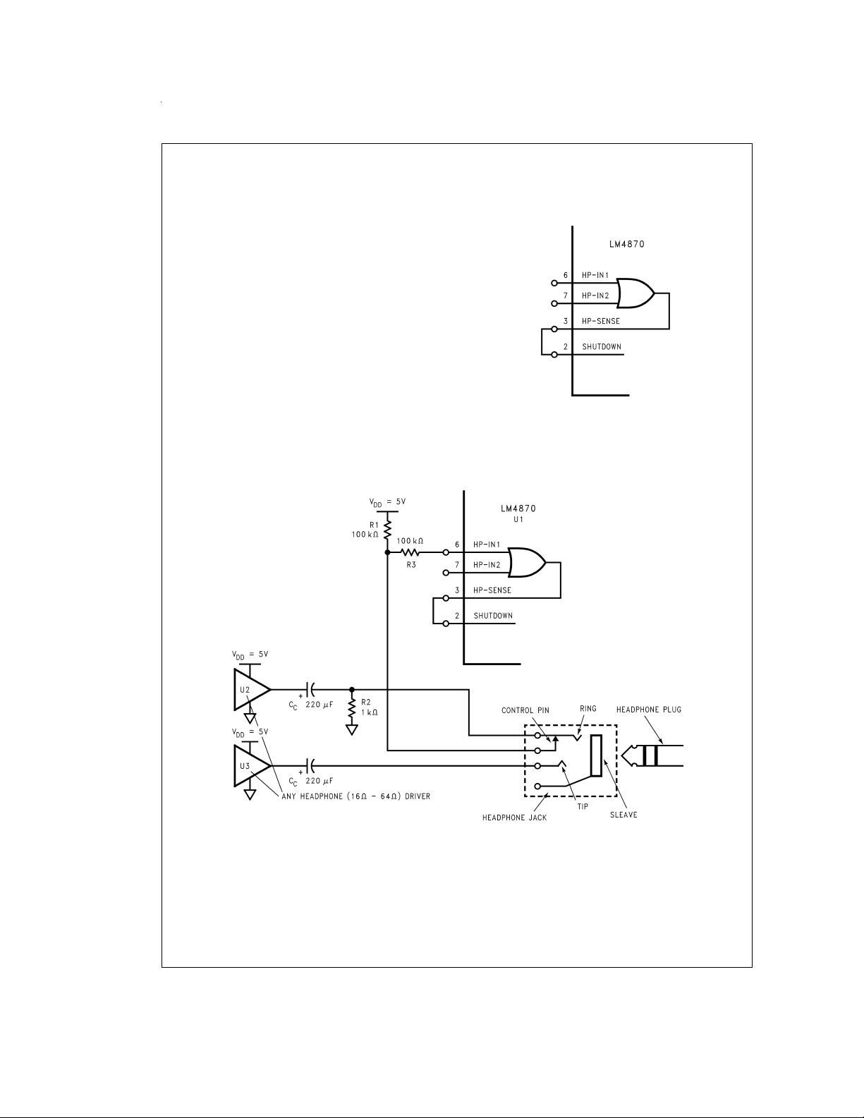
shows the implementation of the LM4870’s headphone control function using a single-supply headphone amplifier. The voltage divider of R1 and R2 sets the voltage at
the HP-IN1 pin to be approximately 50 mV when there are
no headphones plugged into the system. This logic-low voltage at the HP-IN1 pin enables the LM4870 to amplifyAC signals. Resistor R3 limits the amount of current flowing out of
the HP-IN1 pin when the voltage at that pin goes below
ground resulting from the music coming from the headphone
amplifier. The output coupling cap protects the headphones
by blocking the amplifier’s half-supply DC voltage. The capacitor also protects the headphone amplifier from the low
voltage set up by resistors R1 and R2 when there aren’t any
headphones plugged into the system. The tricky point to this
setup is that the AC output voltage of the headphone amplifier cannot exceed the 2.0V HP-IN1 voltage threshold when
there aren’t any headphones plugged into the system, assuming that R1 and R2 are 100k and 1k, respectively. The
LM4870 may not be fully shutdown when this level is ex-
www.national.com5
Page 6
Application Information (Continued)
ceeded momentarily, due to the discharging time constant of
the bias-pin voltage. This time constant is established by the
two 50k resistors (in parallel) with the series bypass capacitor value.
When a set of headphones are plugged into the system, the
contact pin of the headphone jack is disconnected from the
signal pin, interrupting the voltage divider set up by resistors
R1 and R2. Resistor R1 then pulls up the HP-IN1 pin, enabling the headphone function and disabling the LM4870
amplifier. The headphone amplifier then drives the headphones, whose impedance is in parallel with resistor R2.
Since the typical impedance of headphones are 32Ω, resistor R2 has negligible effect on the output drive capability.
Also shown in
headphone jack and plug. A 3-wire plug consists of a Tip,
Ring, and Sleave, where the Tip and Ring are signal carrying
conductors and the Sleave is the common ground return.
One control pin contact for each headphone jack is sufficient
to indicate to control inputs that the user has inserted a plug
into a jack and that another mode of operation is desired.
For a system implementation where the headphone amplifier
is designed using a split supply, the output coupling cap, C
and resistor R2 of
ality described earlier remains the same, however.
Figure 3
are the electrical connections for the
Figure 3
, can be eliminated. The function-
In addition, the HP-SENSE pin, although it may be connected to the SHUTDOWN pin as shown in
still be used as a control flag. It is capable of driving the input
to another logic gate or approximately 2 mA without serious
loading.
DS100094-7
FIGURE 2. HP-SENSE Pin to
SHUTDOWN Pin Connection
C
Figure 2
, may
FIGURE 3. Typical Headphone Control Input Circuitry
AUDIO POWER AMPLIFIER DESIGN
Design a 500 mW/8Ω Audio Amplifier
Given:
Power Output: 1.0Wrms
Load Impedance: 8Ω
Input Level: 1 Vrms(max)
www.national.com 6
DS100094-8
Input Impedance: 20 kΩ
±
Bandwidth: 100 Hz-20 kHz
0.25 dB
A designer must first determine the needed supply rail to obtain the specified output power. The Output Power vs Supply
Voltage graphs in the Typical Performance Characteris-
tics section show how much power the LM4870 will output
given different supply voltage. According to the graph, 4.6V
Page 7
Application Information (Continued)
are required for 1.0W of output power. Since 5V rails are
common, it is chosen to be the supply voltage. Supply voltage (up to a maximum of 5.5V) above the required 4.6V will
allow the LM4870 to reproduce transient signals at greater
than 1.0W of output power. The extra voltage will also increase the device power dissipation, so the designer must
make sure that the conditions explained in the Power Dissi-
pationsection are not violated.
Once the power dissipation issues have been addressed,
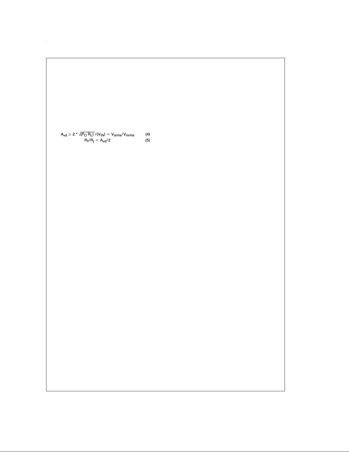
the required differential gain can be determined from Equation 4:
From equation 4, the minimum Avdis A
3.
Since the amplifier output is bridged, giving a gain of 2, and
the desired system gain is 3, the ratio of feedback (R
=
vd
2.83; use A
)toin-
f
vd
put (R
) resistor is 1.5:1. If Riis set to the required input im-
i
pedance of 20 kΩ, then R
to address the bandwidth requirements which must be
=
30 kΩ. The final design step is
f
stated as a pair of −3 dB frequency points. Five times away
from a −3 dB point is 0.17 dB down from passband response
which is better than the required
=
f
100 Hz/5=20 Hz
=
20 kHz5=100 HzAs stated in the External Compo-
f
H
nents section, R
C
≥ 1/(2π*20 kΩ*20 Hz)=0.397 µF; use 0.39 µF.
i
L
in conjunction with Cicreate a highpass
i
±
0.25 dB specified.
filter.
The high frequency pole is determined by the product of the
desired high frequency pole, f
vd
. With a A
150 kHz which is much smaller than the LM4870 GBWP of
=
3 and f
vd
, and the differential gain, A
H
=
100 kHz, the resulting GBWP
H
4 MHz. This figure displays that if a designer has a need to
design an amplifier with a higher differential gain, the
=
LM4870 can still be used without running into bandwidth
problems.
=
www.national.com7
Page 8
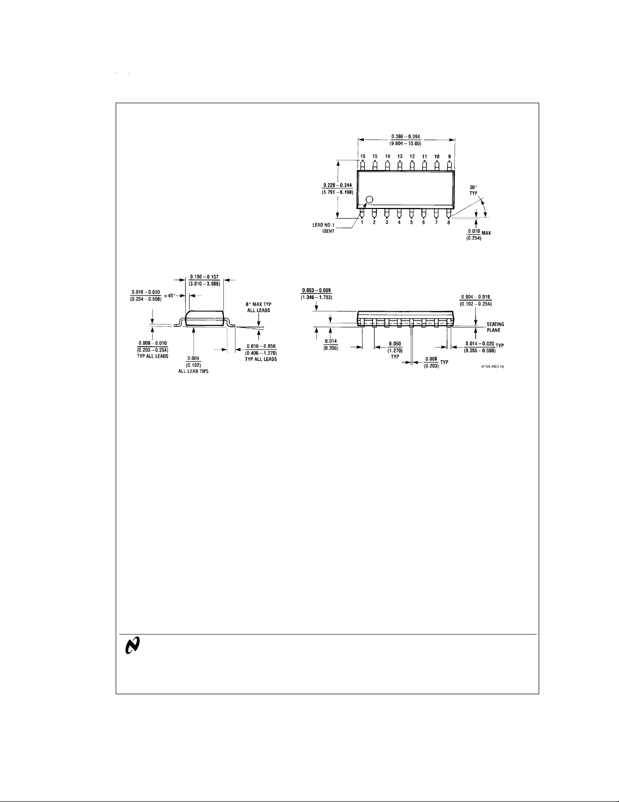
Physical Dimensions inches (millimeters) unless otherwise noted
Small Outline Package (M)
Order Number LM4870M
NS Package Number M16A
LM4870 1.1W Audio Power Amplifier with Shutdown Mode
LIFE SUPPORT POLICY
NATIONAL’S PRODUCTS ARE NOT AUTHORIZED FOR USE AS CRITICAL COMPONENTS IN LIFE SUPPORT
DEVICES OR SYSTEMS WITHOUT THE EXPRESS WRITTEN APPROVAL OF THE PRESIDENT AND GENERAL
COUNSEL OF NATIONAL SEMICONDUCTOR CORPORATION. As used herein:
1. Life support devices or systems are devices or
systems which, (a) are intended for surgical implant
into the body, or (b) support or sustain life, and
whose failure to perform when properly used in
accordance with instructions for use provided in the
labeling, can be reasonably expected to result in a
significant injury to the user.
National Semiconductor
Corporation
Americas
Tel: 1-800-272-9959
Fax: 1-800-737-7018
Email: [email protected]
www.national.com
National does not assume any responsibility for use of any circuitry described, no circuit patent licenses are implied and National reserves the right at any time without notice to change said circuitry and specifications.
National Semiconductor
Europe
Fax: +49 (0) 1 80-530 85 86
Email: [email protected]
Deutsch Tel: +49 (0) 1 80-530 85 85
English Tel: +49 (0) 1 80-532 78 32
Français Tel: +49 (0) 1 80-532 93 58
Italiano Tel: +49 (0) 1 80-534 16 80
2. A critical component is any component of a life
support device or system whose failure to perform
can be reasonably expected to cause the failure of
the life support device or system, or to affect its
safety or effectiveness.
National Semiconductor
Asia Pacific Customer
Response Group
Tel: 65-2544466
Fax: 65-2504466
Email: [email protected]
National Semiconductor
Japan Ltd.
Tel: 81-3-5639-7560
Fax: 81-3-5639-7507
 Loading...