

Page 1
LM4868
Output-Transient-Free Dual 2.1W Audio Amplifier Plus
No Coupling Capacitor Stereo Headphone Function
General Description
The LM4868 is a dual bridge-connected audio power amplifier which, when connected to a 5V supply, will deliver 2.1W
toa4Ω load (Note 1) or 2.4W to a 3Ω load (Note 2) with less
than 1.0% THD+N. The LM4868 uses advanced, latest generation circuitry to eliminate all traces of clicks and pops
when the supply voltage is first applied. The amplifier has a
headphone-amplifier-select input pin. It is used to switch the
amplifiers from bridge to single-ended mode for driving
headphones. A new circuit topology eliminates headphone
output coupling capacitors (patent pending). A MUX control
pin allows selection between the two sets of stereo input
signals. The MUX control can also be used to select between two different customer-specified closed-loop responses.
Boomer audio power amplifiers are designed specifically to
provide high quality output power from a surface mount
package and require few external components. To simplify
audio system design, the LM4868 combines dual bridge
speaker amplifiers and stereo headphone amplifiers in one
package.
The LM4868 features an externally controlled power-saving
micropower shutdown mode, a stereo headphone amplifier
mode, and thermal shutdown protection.
Note 1: An LM4868LQ or LM4868MTE that has been properly mounted to
a circuit board will deliver 2.1W into 4Ω. The Mux control can also be used to
select two different closed-loop responses. LM4868MT will deliver 1.1W into
8Ω. See the Application Information sections for further information concerning the LM4868LQ and the LM4868MT.
Note 2: An LM4868LQ or LM4868MTE that has been properly mounted to a
circuit board and forced-air cooled will deliver 2.4W into 3Ω.
Key Specifications
n POat 1% THD+N
n LM4868LQ, 3Ω load 2.4W (typ)
n LM4868LQ, 4Ω load 2.1W (typ)
n LM4868MTE, 4Ω 1.9W (typ)
n LM4868MT, 8Ω 1.1W (typ)
n Single-ended mode - THD+N at 75mW into 32Ω 0.5%
(max)
n Shutdown current 0.7µA (typ)
Features
n Advanced “click and pop” suppression circuitry
n Eliminates headphone amplifier output coupling
capacitors (patent pending)
n Stereo headphone amplifier mode
n Input mux control and two separate inputs per channel
n Thermal shutdown protection circuitry
n LLP, TSSOP, and exposed-DAP TSSOP packaging
available
Applications
n Multimedia monitors
n Portable and desktop computers
n Portable audio systems
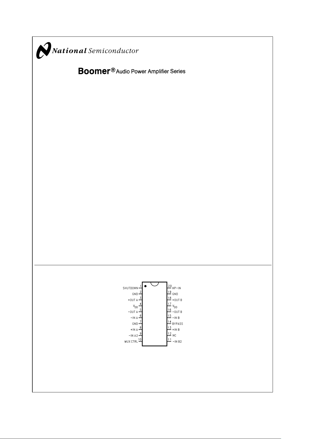
Connection Diagrams
20026758
Top View
Order Number LM4868MT, LM4868MTE
See NS Package Number MTC20 for TSSOP
See NS Package Number MXA20A for Exposed-DAP TSSOP
Boomer®is a registered trademark of National Semiconductor Corporation.
August 2002
LM4868 Output-Transient-Free Dual 2.1W Audio Amplifier Plus No Coupling Capacitor Stereo
Headphone Function
© 2002 National Semiconductor Corporation DS200267 www.national.com
Page 2
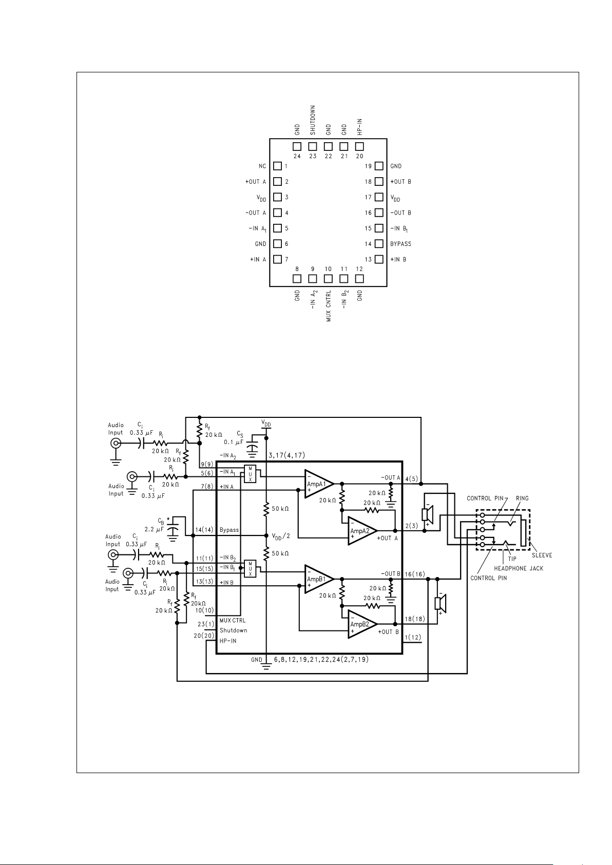
Connection Diagrams (Continued)
20026738
Top View
Order Number LM4868LQ
See NS Package Number LQA24A for Exposed-DAP LLP
Typical Application
20026731
*
Refer to the Application Information section titled PROPER SELECTION OF EXTERNAL COMPONENTS for details concerning the value of CB.
FIGURE 1. Typical Audio Amplifier Application Circuit (Pin out shown for the 24-pin Exposed-DAP LLP package.
Numbers in ( ) are for the 20-pin MTE and MT packages.)
LM4868
www.national.com 2
Page 3
Absolute Maximum Ratings (Note 3)
If Military/Aerospace specified devices are required,
please contact the National Semiconductor Sales Office/
Distributors for availability and specifications.
Supply Voltage 6.0V
Storage Temperature −65˚C to +150˚C
Input Voltage −0.3V to V
DD
+0.3V
Power Dissipation (Note 4) Internally limited
ESD Susceptibility (Note 5)
All pins except Pin 3 (MT, MTE), Pin 2 (LQ) 2000V
Pin 3 (MT, MTE), Pin 2 (LQ) 8000V
ESD Susceptibility (Note 6) 200V
Junction Temperature 150˚C
Solder Information
Small Outline Package
Vapor Phase (60 sec.) 215˚C
Infrared (15 sec.) 220˚C
See AN-450 “Surface Mounting and their Effects on
Product Reliablilty” for other methods of soldering
surface mount devices.
Thermal Resistance
θ
JC
(typ) — MTC20 20˚C/W
θ
JA
(typ) — MTC20 80˚C/W
θ
JC
(typ) — MXA20A 2˚C/W
θ
JA
(typ) — MXA20A 41˚C/W (Note 7)
θ
JA
(typ) — MXA20A 51˚C/W (Note 8)
θ
JA
(typ) — MXA20A 90˚C/W (Note 9)
θ
JC
(typ) — LQA24A 3.0˚C/W
θ
JA
(typ) — LQA24A 42˚C/W (Note 10)
Operating Ratings
Temperature Range
T
MIN
≤ TA≤ T
MAX
−40˚C ≤ TA≤ 85˚C
Supply Voltage 2.0V ≤ V
DD
≤ 5.5V
Electrical Characteristics for Entire IC (Notes 3, 11)
The following specifications apply for VDD= 5V unless otherwise noted. Limits apply for TA= 25˚C.
Symbol Parameter Conditions LM4868 Units
(Limits)
Typical Limit
(Note 12) (Note 13)
V
DD
Supply Voltage 2 V (min)
5.5 V (max)
I
DD
Quiescent Power Supply Current VIN= 0V, IO= 0A (Note 14), HP-IN = 0V 7.5 15 mA (max)
V
IN
= 0V, IO= 0A (Note 14), HP-IN = 4V 3.0 6 mA (max)
I
SD
Shutdown Current VDDapplied to the SHUTDOWN pin 0.7 2 µA (max)
TH
um
Un-Mute Threshold Voltage GND applied to SHUTDOWN pin
V
IN
applied to selected MUX channel
25 10
40
mV (min)
mV (max)
Electrical Characteristics for Bridged-Mode Operation (Notes 3, 11)
The following specifications apply for VDD= 5V unless otherwise specified. Limits apply for TA= 25˚C.
Symbol Parameter Conditions LM4868 Units
(Limits)
Typical Limit
(Note 12) (Note 13)
V
OS
Output Offset Voltage VIN= 0V 5 50 mV (max)
P
O
Output Power (Note 15) THD = 1%, f = 1kHz
(Note 16)
LM4868MTE, R
L
=3Ω 2.2 W
LM4868LQ, R
L
=3Ω 2.4 W
LM4868MTE, R
L
=4Ω 1.9 W
LM4868LQ, R
L
=4Ω 2.1 W
LM4868, R
L
=8Ω 1.1 1.0 W (min)
THD+N = 10%, f = 1kHz (Note 16)
LM4868MTE, R
L
=3Ω 3.0 W
LM4868LQ, R
L
=3Ω 3.0 W
LM4868MTE, R
L
=4Ω 2.6 W
LM4868LQ, R
L
=4Ω 2.6 W
LM4868, R
L
=8Ω 1.5 W
THD+N = 1%, f = 1 kHz, R
L
=32Ω 0.34 W
LM4868
www.national.com3
Page 4
Electrical Characteristics for Bridged-Mode Operation (Notes 3, 11) (Continued)
The following specifications apply for VDD= 5V unless otherwise specified. Limits apply for TA= 25˚C.
Symbol Parameter Conditions LM4868 Units
(Limits)
Typical Limit
(Note 12) (Note 13)
THD+N Total Harmonic Distortion+Noise 20Hz ≤ f ≤ 20kHz, A
VD
=2
LM4868MTE, R
L
=4Ω,PO=2W
LM4868LQ, R
L
=4Ω,PO=2W
LM4868, R
L
=8Ω,PO=1W
0.3
0.3
0.3
%
%
%
PSRR Power Supply Rejection Ratio V
DD
= 5V, V
RIPPLE
= 200 mV
RMS,RL
=8Ω,
C
B
= 2.2µF
67 dB
X
TALK
Channel Separation f = 1 kHz, CB= 2.2µF 80 dB
SNR Signal To Noise Ratio V
DD
= 5V, PO= 1.1W, RL=8Ω 97 dB
Electrical Characteristics for Single-Ended Operation (Notes 3, 11)
The following specifications apply for VDD= 5V unless otherwise specified. Limits apply for TA= 25˚C.
Symbol Parameter Conditions LM4868 Units
(Limits)
Typical Limit
(Note 12) (Note 13)
V
OS
Output Offset Voltage VIN= 0V 5 50 mV (max)
P
O
Output Power THD = 0.5%, f = 1kHz, RL=32Ω 85 75 mW (min)
THD+N = 1%, f = 1kHz, R
L
=8Ω (Note
17)
180 mW
THD+N = 1%, f = 1kHz, R
L
=16Ω
THD+N = 1%, f = 1kHz, R
L
=32Ω
THD+N = 10%, f = 1kHz, R
L
=16Ω
THD+N = 10%, f = 1kHz, R
L
=32Ω
165
88
208
114
mW
mW
mW
mW
V
OUT
Output Voltage Swing THD = 0.05%, RL=5kΩ 1V
P-P
THD+N Total Harmonic Distortion+Noise AV= −1, PO= 75mW, 20 Hz ≤ f ≤ 20kHz,
R
L
=32Ω
0.2 %
PSRR Power Supply Rejection Ratio C
B
= 2.2µF, V
RIPPLE
= 200mV
RMS
,
f = 1kHz
52 dB
X
TALK
Channel Separation f = 1kHz, CB= 2.2µF 60 dB
SNR Signal To Noise Ratio V
DD
= 5V, PO= 340mW, RL=8Ω 94 dB
Note 3: Absolute Maximum Ratings indicate limits beyond which damage to the device may occur. Operating Ratings indicate conditions for which the device is
functional, but do not guarantee specific performance limits. Electrical Characteristics state DC and AC electrical specifications under particular test conditions which
guarantee specific performance limits. This assumes that the device operates within the Operating Ratings. Specifications are not guaranteed for parameters where
no limit is given. The typical value however, is a good indication of device performance.
Note 4: The maximum power dissipation must be derated at elevated temperatures and is dictated by T
JMAX
, θJA, and the ambient temperature TA. The maximum
allowable power dissipation is P
DMAX
=(T
JMAX−TA
)/θJA. For the LM4868, T
JMAX
= 150˚C. For the θJAs for different packages, please see the Application
Information section or the Absolute Maximum Ratings section.
Note 5: Human body model, 100pF discharged through a 1.5kΩ resistor.
Note 6: Machine model, 220pF–240pF discharged through all pins.
Note 7: The given θ
JA
is for an LM4868 packaged in an MXA20A with the Exposed-DAP soldered to an exposed 2in2area of 1oz printed circuit board copper.
Note 8: The given θ
JA
is for an LM4868 packaged in an MXA20A with the Exposed-DAP soldered to an exposed 1in2area of 1oz printed circuit board copper.
Note 9: The given θ
JA
is for an LM4868 packaged in an MXA20A with the Exposed-DAP not soldered to printed circuit board copper.
Note 10: The given θ
JA
is for an LM4868 packaged in an LQA24A with the Exposed-DAP soldered to an exposed 2in2area of 1oz printed circuit board copper.
Note 11: All voltages are measured with respect to the ground (GND) pins, unless otherwise specified.
Note 12: Typicals are measured at 25˚C and represent the parametric norm.
Note 13: Limits are guaranteed to National’s AOQL (Average Outgoing Quality Level). Datasheet min/max specification limits are guaranteed by design, test, or
statistical analysis.
Note 14: The quiescent power supply current depends on the offset voltage when a practical load is connected to the amplifier.
Note 15: Output power is measured at the device terminals.
Note 16: When driving 3Ω or 4Ω loads and operating on a 5V supply, the LM4868LQ and LM4868MTE must be mounted to a circuit board that has a minimum of
2.5in
2
of exposed, uniterrupted copper area connected to the LLP or TSSOP package’s exposed DAP.
Note 17: See Application Information section ’Single-Ended Output Power Performance and Measurement Considerations’ for more information.
LM4868
www.national.com 4
Page 5
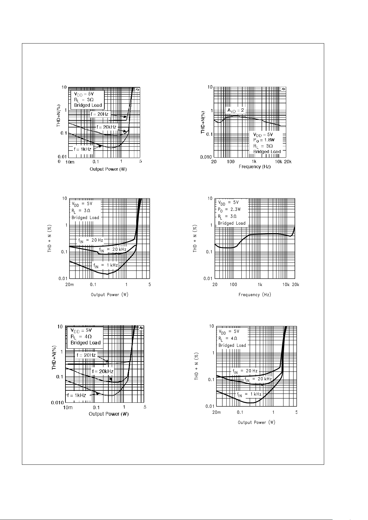
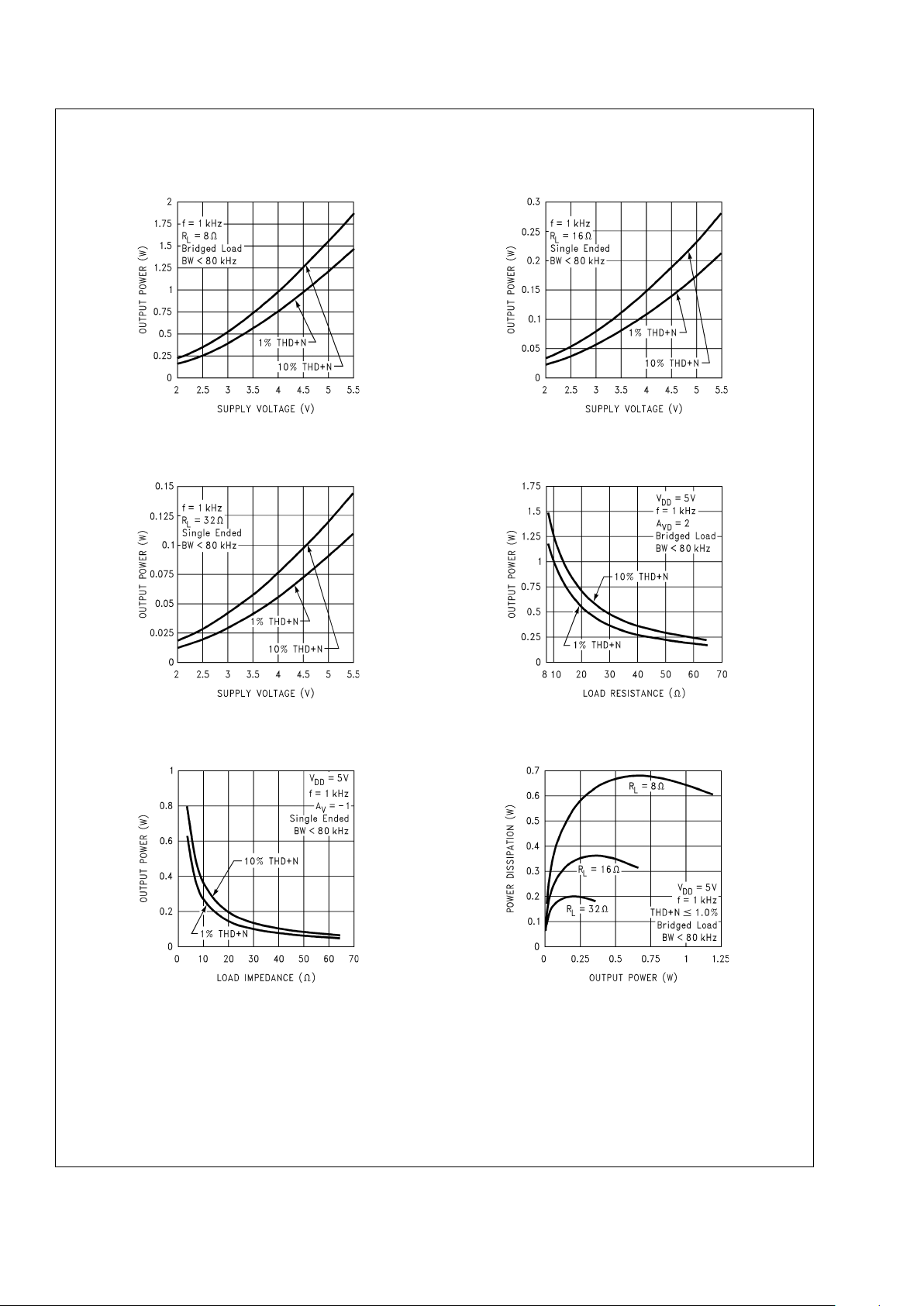
Typical Performance Characteristics
MTE- and LQ- Specific Characteristics
LM4868MTE
THD+N vs Output Power
LM4868MTE
THD+N vs Frequency
20026733
20026734
LM4868LQ
THD+N vs Output Power
LM4868LQ
THD+N vs Frequency
20026753 20026754
LM4868MTE
THD+N vs Output Power
LM4868LQ
THD+N vs Output Power
20026736
20026755
LM4868
www.national.com5
Page 6
Typical Performance Characteristics
MTE- and LQ- Specific Characteristics
(Continued)
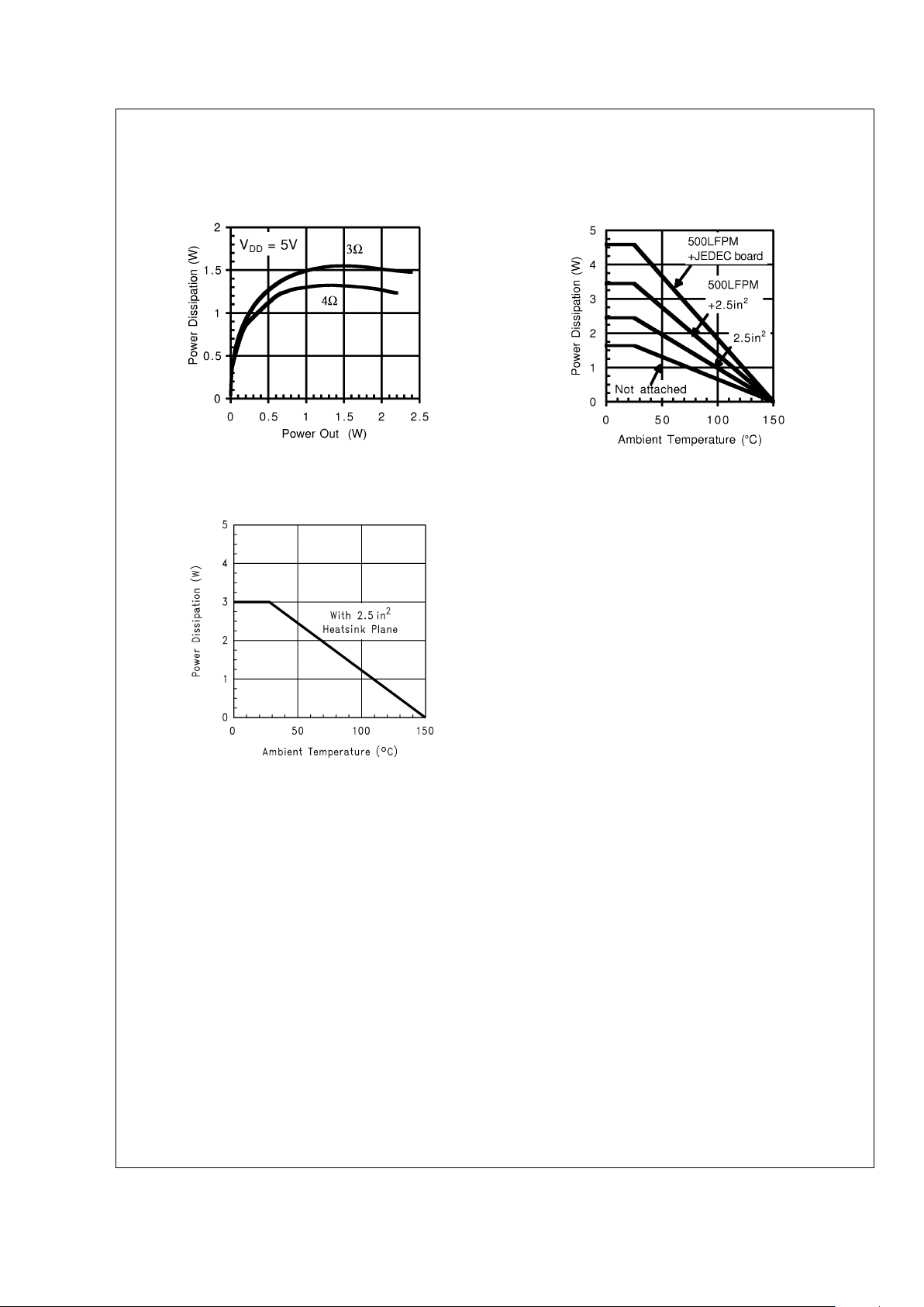
LM4868LQ, LM4868MTE
Power Dissipation vs Power Output
LM4868MTE (Note 18)
Power Derating Curve
20026761
20026759
LM4868LQ
Power Derating Curve
20026769
Note 18: This curve shows the LM4868MTE’s thermal dissipation ability at different ambient temperatures given these conditions:
500LFPM + JEDEC board: The part is soldered to a 1S2P 20-lead exposed-DAP TSSOP test board with 500 linear feet per minute of forced-air flow across
it. Board information - copper dimensions: 74x74mm, copper coverage: 100% (buried layer) and 12% (top/bottom layers), 16 vias under the exposed-DAP.
500LFPM + 2.5in
2
: The part is soldered to a 2.5in2, 1 oz. copper plane with 500 linear feet per minute of forced-air flow across it.
2.5in
2
: The part is soldered to a 2.5in2, 1oz. copper plane.
Not Attached: The part is not soldered down and is not forced-air cooled.
LM4868
www.national.com 6
Page 7
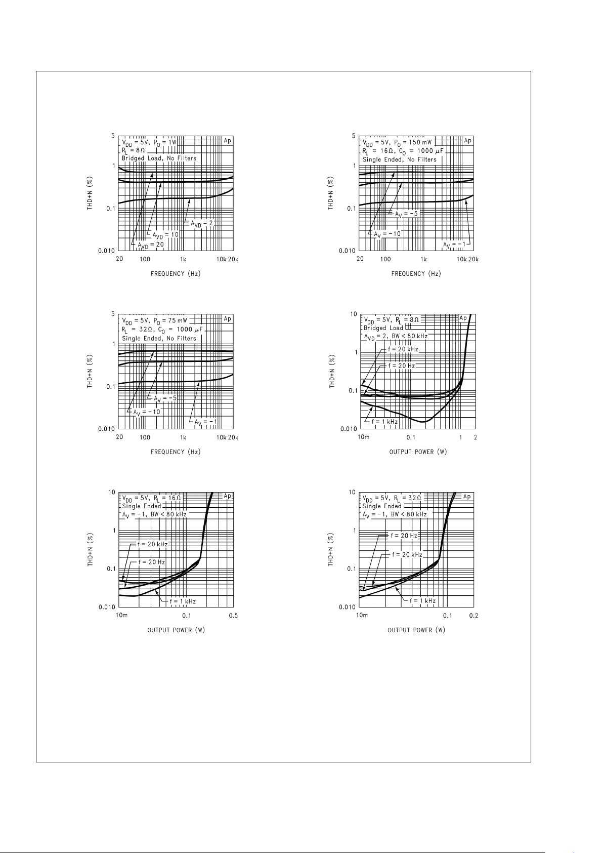
Typical Performance
Characteristics
THD+N vs Frequency THD+N vs Frequency
20026703 20026704
THD+N vs Frequency THD+N vs Output Power
20026705 20026706
THD+N vs Output Power THD+N vs Output Power
20026707 20026708
LM4868
www.national.com7
Page 8
Typical Performance Characteristics (Continued)
THD+N vs Output Power THD+N vs Frequency
20026765
20026763
THD+N vs Output Power THD+N vs Frequency
20026766 20026764
Output Power vs
Load Resistance
Power Dissipation vs
Supply Voltage
20026762
20026760
LM4868
www.national.com 8
Page 9
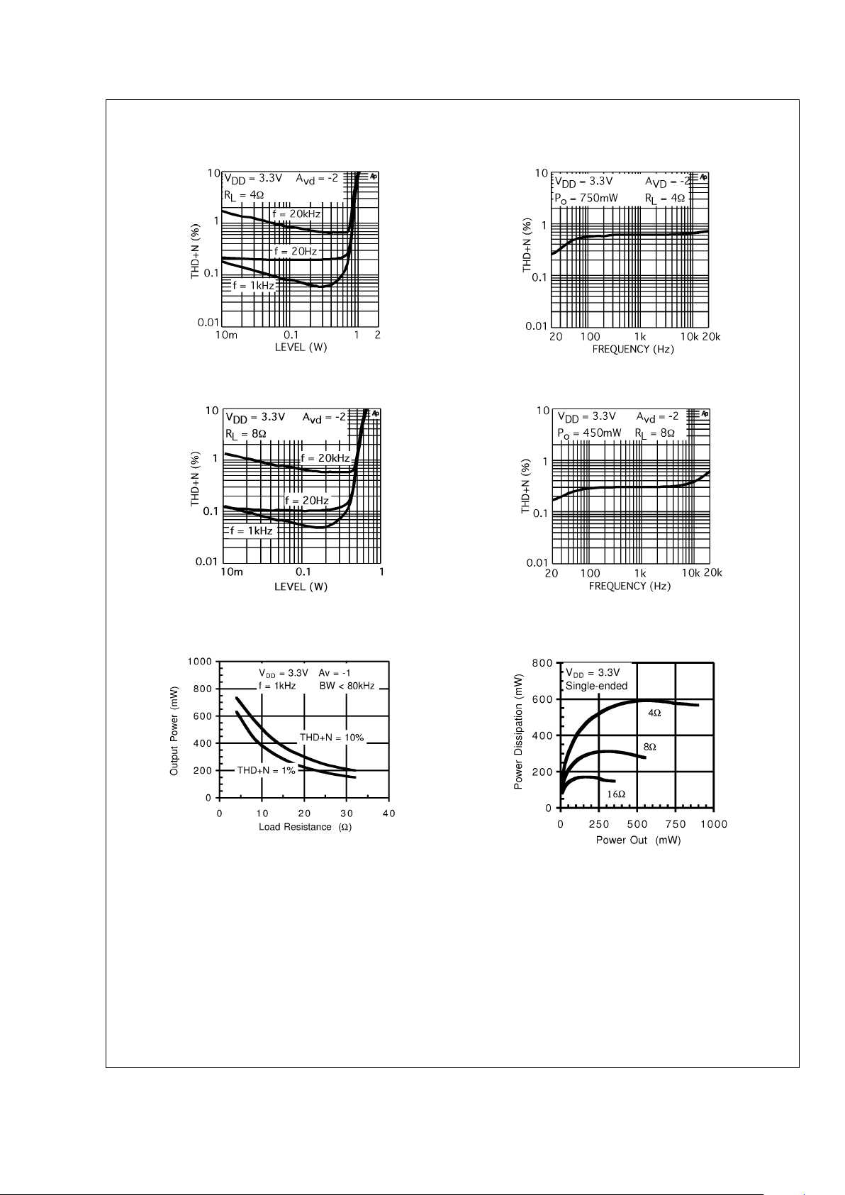
Typical Performance Characteristics (Continued)
Output Power vs
Supply Voltage
Output Power vs
Supply Voltage
20026709 20026710
Output Power vs
Supply Voltage
Output Power vs
Load Resistance
20026711
20026712
Output Power vs
Load Resistance
Power Dissipation vs
Output Power
20026713 20026714
LM4868
www.national.com9
Page 10

Typical Performance Characteristics (Continued)
Dropout Voltage vs
Supply Voltage Power Derating Curve
20026715
20026716
Power Dissipation vs
Output Power Noise Floor
20026717
20026718
Channel Separation Channel Separation
20026719
20026720
LM4868
www.national.com 10
Page 11

Typical Performance Characteristics (Continued)
Power Supply
Rejection Ratio
Open Loop
Frequency Response
20026721 20026722
Supply Current vs
Supply Voltage
20026723
External Components Description
( Refer to Figure 1. )
Components Functional Description
1. R
i
This is the inverting input resistance that sets the closed-loop gain in conjunction with Rf. This resistor also
forms a high pass filter with C
i
at fc= 1/(2πRiCi).
2. C
i
This is the input coupling capacitor. It blocks the DC voltage at the amplifier’s input terminals. It also
creates a highpass filter with R
i
at fc= 1/(2πRiCi). Refer to the section, Selecting External Components,
for an explanation of how to determine the value of C
i
.
3. R
f
This is the feedback resistance. It sets the closed-loop gain in conjunction with Ri.
4. C
s
This is the supply bypass capacitor. It provides power supply filtering. Refer to the Power Supply
Bypassing section for information concerning proper placement and selection of the supply bypass
capacitor.
5. C
B
This is the bypass pin capacitor. It provides half-supply filtering. Refer to the section, Proper Selection of
External Components, for information concerning proper placement and selection of C
B
.
Application Information
ELIMINATING OUTPUT COUPLING CAPACITORS
Typical single-supply audio amplifiers that can switch between driving bridge-tied-load (BTL) speakers and
single-ended (SE) headphones use a coupling capacitor on
each SE output. This capacitor blocks the half-supply voltage to which the output amplifiers are typically biased and
couples the audio signal to the headphones. The signal
return to circuit ground is through the headphone jack’s
sleeve.
The LM4868 eliminates these coupling capacitors. Amp2A is
internally configured to apply V
DD
/2 to a stereo headphone
jack’s sleeve. This voltage matches the quiescent voltage
present on the Amp1A and Amp1B outputs that drive the
LM4868
www.national.com11
Page 12

Application Information (Continued)
headphones. The headphones operate in a manner very
similar to a bridge-tied-load (BTL). The same DC voltage is
applied to both headphone speaker terminals. This results in
no net DC current flow through the speaker. AC current flows
through a headphone speaker as an audio signal’s output
amplitude increases on the speaker’s terminal.
When operating as a headphone amplifier, the headphone
jack sleeve is not connected to circuit ground. Using the
headphone output jack as a line-level output will place the
LM4868’s one-half supply voltage on a plug’s sleeve connection. Driving a portable notebook computer or
audio-visual display equipment is possible. This presents no
difficulty when the external equipment uses capacitively
coupled inputs. For the very small minority of equipment that
is DC-coupled, the LM4868 monitors the current supplied by
the amplifier that drives the headphone jack’s sleeve. If this
current exceeds 500mA
PK
, the amplifier is shutdown, protecting the LM4868 and the external equipment. For more
information, see the section titled ’Single-Ended Output
Power Performance and Measurement Considerations’.
OUTPUT TRANSIENT (’POPS AND CLICKS’)
ELIMINATED
The LM4868 contains advanced circuitry that eliminates output transients (’pop and click’). This circuitry prevents all
traces of transients when the supply voltage is first applied,
when the part resumes operation after shutdown, or when
switching between BTL speakers and SE headphones. Two
circuits combine to eliminate pop and click. One circuit
mutes the output when switching between speaker loads.
Another circuit monitors the input signal. It maintains the
muted condition until there is sufficient input signal magnitude (
>
25mV
RMS
, typ) to mask any remaining transient that
may occur.
Figure 2 shows the LM4868’s lack of transients in the differential signal (Trace B) across a BTL 8Ω load. The LM4868’s
active-high SHUTDOWN pin is driven by the logic signal
shown in Trace A. Trace C is the VOUT- output signal and
trace D is the VOUT+ output signal. The shutdown signal
frequency is 1Hz with a 50% duty cycle. Figure 3 is generated with the same conditions except that the output drives a
32Ω single-ended (SE) load. Again, no trace of output transients is seen.
USING THE LM4868 TO UPGRADE LM4863 AND LM4873
DESIGNS
The LM4868’s noise-free operation plus
coupling-capacitorless headphone operation and functional
compatibility with the LM4873 and the LM4863 simplifies
upgrading systems using these parts. Upgrading older designs that use either the LM4863 or the LM4873 is easy.
Simply remove and short the coupling capacitors located
between the LM4873’s or LM4863’s Amp1A and Amp1B
outputs and the headphone connections. Also remove the
1kΩ resistor between each headphone connection and
ground. Finally, remove any resistors connected to the
HP-IN pin (typically two 100kΩ resistors). Connect the HP-IN
pin directly to the headphone jack control pin as shown in
Figure 4.
The LM4868’s pin configuration simplifies the process of
upgrading systems that use the LM4863. Except for its four
MUX function pins, the LM4868’s pin configuration matches
the LM4863’s pin configuration. If the LM4868’s MUX functionality is not needed when replacing an LM4863, connect
the MUX CTRL pin to either V
DD
or ground. To ensure
correct amplifier operation, unused MUX inputs should be
tied to GND. As shown in Table 1, grounding the MUX CTRL
pin selects stereo input 1 (−IN A1 and −IN B1), whereas
applying V
DD
to the MUX CTRL pin selects stereo input 2
(−IN A2 and −IN B2).
The LM4868’s unique headphone sense circuit requires a
dual switch headphone jack. Replace the four-terminal headphone jack used with the LM4863 and LM4873 with the
five-terminal headphone jack, such as the Switchcraft
35RAPC4BH3, shown in Figure 4. Connect the +OUT A
(Amp2A) pin to the five-terminal headphone jack’s sleeve
pin.
20026756
FIGURE 2. Differential output signal (Trace B) is devoid
of transients. The SHUTDOWN pin is driven by a
shutdown signal (Trace A). The inverting output (Trace
C) and the non-inverting output (Trace D) are applied
across an 8Ω BTL load.
20026757
FIGURE 3. Single-ended output signal (Trace B) is
devoid of transients. The SHUTDOWN pin is driven by
a shutdown signal (Trace A). The inverting output
(Trace C) and the V
BYPASS
output (Trace D) are applied
across a 32Ω BTL load.
LM4868
www.national.com 12
Page 13

Application Information (Continued)
STEREO-INPUT MULTIPLEXER (STEREO MUX)
The LM4868 has two stereo inputs. The MUX CTRL Pin
controls which stereo input is active. As shown in the Truth
Table for Logic Inputs, applying 0V to the MUX CTRL input
activates stereo input 1, whereas applying V
DD
to the MUX
CTRL inputs activates stereo input 2. To ensure correct
amplifier operation, unused MUX inputs should be tied to
GND.
Typical LM4868 applications use the MUX to switch between
two stereo input signals. Each stereo channel’s gain can be
tailored to produce the required output signal level by choosing the appropriate input and feedback resistor ratio.
Another configuration uses the MUX to select two different
gains or frequency compensated gains that amplify a single
pair of stereo input signals. Figure 5 shows two different
feedback networks, Network 1 and Network 2. Network 1
produces increasing gain as the input signal’s frequency
decreases. This can be used to compensate a small,
full-range speaker’s low frequency response roll-off. Network
2 sets the gain for an alternate load such as headphones.
The circuit in Figure 6 uses Network 1 when driving external
speakers, switching to Network 2 when headphones are
connected. The normally closed control switch in Figure 6’s
headphone jack connects to the MUX CTRL pin. When
headphones are connected, the LM4868’s internal pull-up
that applies V
DD
to the HP-IN and the external 100kΩ resis-
tor applies V
DD
to MUX CTRL pin. Simultaneously applying
these control voltages automatically selects the amplifier
(headphone or bridge) and switches the gain (MUX channel
selection). Alternatively, leaving the MUX CTRL pin independently accessible allows a user to select bass boost as
needed. This alternative user-selectable bass-boost scheme
requires connecting equal ratio resistor feedback networks
to each MUX input channel. The value of the resistor in the
RC network is chosen to give a gain that is necessary to
achieve the desired bass-boost.
Switching between the MUX channels may change the input
signal source or the feedback resistor network. During the
channel switching transition, the average voltage level
20026731
FIGURE 4. Typical Audio Amplifier Application Circuit
(Pin out shown for the 24-pin Exposed-DAP LLP package. Numbers in ( ) are for the 20-pin MTE and MT packages.)
20026728
FIGURE 5. Input MUX Example
LM4868
www.national.com13
Page 14

Application Information (Continued)
present on the internal amplifier’s input may change. This
change can slew at a rate that may produce audible voltage
transients or clicks in the amplifier’s output signal. Using the
MUX to select between two vastly dissimilar gains is a typical
transient-producing situation. As the MUX is switched, an
audible click may occur as the gain suddenly changes.
PIN OUT COMPATIBILITY WITH THE LM4863
The LM4868 pin out was designed to simplify replacing the
LM4863: except for the four Pins(-IN A
2
, MUX CTRL, -IN B2,
and NC) that implement the LM4868’s extra functionality, the
LM4868MT/MTE and LM4863MT/MTE pin outs match.
(Note 19)
Note 19: If the LM4868 replaces an LM4863 and the input MUX circuitry is
not being used, the LM4868 MUX CTRL pin must be tied to V
DD
or GND and
the unused MUX inputs must be connected to GND.
EXPOSED-DAP MOUNTING CONSIDERATIONS
The LM4868’s exposed-DAP (die attach paddle) packages
(MTE and LQ) provide a low thermal resistance between the
die and the PCB to which the part is mounted and soldered.
This allows rapid heat transfer from the die to the surrounding PCB copper area heatsink, copper traces, ground plane,
and finally, surrounding air. The result is a low voltage audio
power amplifier that produces 2.4W dissipation in a 4Ω load
at ≤ 1% THD+N and over 3W in a 3Ω load at 10% THD+N.
This high power is achieved through careful consideration of
necessary thermal design. Failing to optimize thermal design
may compromise the LM4868’s high power performance and
activate unwanted, though necessary, thermal shutdown
protection.
The MTE and LQ packages must have their DAPs soldered
to a copper pad on the PCB. The DAP’s PCB copper pad is
then, ideally, connected to a large plane of continuous unbroken copper. This plane forms a thermal mass, heat sink,
and radiation area. Place the heat sink area on either outside
plane in the case of a two-sided or multi-layer PCB. (The
heat sink area can also be placed on an inner layer of a
multi-layer board. The thermal resistance, however, will be
higher.) Connect the DAP copper pad to the inner layer or
backside copper heat sink area with 32 (4 X 8) (MTE) or 6 (3
X 2) (LQ) vias. The via diameter should be 0.012in - 0.013in
with a 1.27mm pitch. Ensure efficient thermal conductivity by
plugging and tenting the vias with plating and solder mask,
respectively.
Best thermal performance is achieved with the largest practical copper heat sink area. If the heatsink and amplifier
share the same PCB layer, a nominal 2.5in
2
(min) area is
necessary for 5V operation with a 4Ω load. Heatsink areas
not placed on the same PCB layer as the LM4868 should be
5in
2
(min) for the same supply voltage and load resistance.
The last two area recommendations apply for 25˚C ambient
temperature. Increase the area to compensate for ambient
temperatures above 25˚C. In systems using cooling fans, the
LM4868MTE can take advantage of forced air cooling. With
an air flow rate of 450 linear-feet per minute and a 2.5in
2
exposed copper or 5.0in2inner layer copper plane heatsink,
the LM4868MTE can continuously drive a 3Ω load to full
power. The LM4868LQ achieves the same output power
level without forced-air cooling. In all circumstances and
under all conditions, the junction temperature must be held
below 150˚C to prevent activating the LM4868’s thermal
shutdown protection. The LM4868’s power de-rating curve in
the Typical Performance Characteristics shows the maximum power dissipation versus temperature. Example PCB
layouts for the exposed-DAP TSSOP and LQ packages are
shown in the Demonstration Board Layout section. Further
detailed and specific information concerning PCB layout and
fabrication and mounting an LQ (LLP) is found in National
Semiconductor’s AN1187.
PCB LAYOUT AND SUPPLY REGULATION
CONSIDERATIONS FOR DRIVING 3Ω AND 4Ω LOADS
Power dissipated by a load is a function of the voltage swing
across the load and the load’s impedance. As load impedance decreases, load dissipation becomes increasingly dependent on the interconnect (PCB trace and wire) resistance
between the amplifier output pins and the load’s connections. Residual trace resistance causes a voltage drop,
which results in power dissipated in the trace and not in the
load as desired. For example, 0.1Ω trace resistance reduces
the output power dissipated by a 4Ω load from 2.1W to 2.0W.
The problem of decreased load dissipation is exacerbated
as load impedance decreases. Therefore, to maintain the
highest load dissipation and widest output voltage swing,
PCB traces that connect the output pins to a load must be as
wide as possible.
Poor power supply regulation adversely affects maximum
output power. A poorly regulated supply’s output voltage
decreases with increasing load current. Reduced supply
voltage causes decreased headroom, output signal clipping,
and reduced output power. Even with tightly regulated supplies, trace resistance creates the same effects as poor
supply regulation. Therefore, making the power supply
traces as wide as possible helps maintain full output voltage
swing.
BRIDGE CONFIGURATION EXPLANATION
As shown in Figure 4, the LM4868 consists of two pairs of
operational amplifiers, forming a two-channel (channel A and
channel B) stereo amplifier. (Though the following discusses
channel A, it applies equally to channel B.) External resistors
R
f
and Riset the closed-loop gain of Amp1A, whereas two
internal 20kΩ resistors set Amp2A’s gain at -1. The LM4868
drives a load, such as a speaker, connected between the two
amplifier outputs, -OUTA and +OUTA.
Figure 4 shows that Amp1A’s output serves as Amp2A’s
input. This results in both amplifiers producing signals iden-
20026739
FIGURE 6. As configured, connecting headphones to
this jack automatically selects the stereo headphone
amplifier and, with the additional NC switch, changes
MUX channels (Network 2 in Figure 5 )
LM4868
www.national.com 14
Page 15

Application Information (Continued)
tical in magnitude, but 180˚ out of phase. Taking advantage
of this phase difference, a load is placed between -OUTA
and +OUTA and driven differentially (’commonly referred to
as bridge mode’). This results in a differential gain of
A
VD
=2*(Rf/Ri) (1)
Bridge mode amplifiers are different from single-ended amplifiers that drive loads connected between a single amplifier’s output and ground. For a given supply voltage, bridge
mode has a distinct advantage over the single-ended configuration: its differential output doubles the voltage swing
across the load. This produces four times the output power
when compared to a single-ended amplifier under the same
conditions. This increase in attainable output power assumes that the amplifier is not current limited or that the
output signal is not clipped. To ensure minimum output signal clipping when choosing an amplifier’s closed-loop gain,
refer to the Audio Power Amplifier Design section.
Another advantage of the differential bridge output is no net
DC voltage across the load. This is accomplished by biasing
channel A’s and channel B’s outputs at half-supply. This
eliminates the coupling capacitor that single supply,
single-ended amplifiers require. Eliminating an output coupling capacitor in a single-ended configuration forces a
single-supply amplifier’s half-supply bias voltage across the
load. This increases internal IC power dissipation and may
permanently damage loads such as speakers.
POWER DISSIPATION
Power dissipation is a major concern when designing a
successful single-ended or bridged amplifier. Equation (2)
states the maximum power dissipation point for a
single-ended amplifier operating at a given supply voltage
and driving a specified output load.
P
DMAX
=(VDD)2/(2π2RL): Single-Ended (2)
However, a direct consequence of the increased power delivered to the load by a bridge amplifier is higher internal
power dissipation for the same conditions.
The LM4868 has two operational amplifiers per channel. The
maximum internal power dissipation per channel operating in
the bridge mode is four times that of a single-ended amplifier. From Equation (3), assuming a 5V power supply and an
4Ω load, the maximum single channel power dissipation is
1.27W or 2.54W for stereo operation.
P
DMAX
=4*(VDD)2/(2π2RL): Bridge Mode (3)
The LM4868’s power dissipation is twice that given by Equation (2) or Equation (3) when operating in the single-ended
mode or bridge mode, respectively. Twice the maximum
power dissipation point given by Equation (3) must not exceed the power dissipation given by Equation (4):
P
DMAX
’=(T
JMAX−TA
)/θ
JA
(4)
The LM4868’s TJMAX = 150˚C. In the LQ package soldered
to a DAP pad that expands to a copper area of 5in
2
on a
PCB, the LM4868’s θ
JA
is 42˚C/W. In the MTE package
soldered to a DAP pad that expands to a copper area of 2in
2
on a PCB, the LM4868’s θJAis 41˚C/W. At any given ambient
temperature T
A
, use Equation (4) to find the maximum internal power dissipation supported by the IC packaging. Rearranging Equation (4) and substituting P
DMAX
for P
DMAX
’ results in Equation (5). This equation gives the maximum
ambient temperature that still allows maximum stereo power
dissipation without violating the LM4868’s maximum junction
temperature.
T
A=TJMAX
−2XP
DMAXθJA
(5)
For a typical application with a 5V power supply and an 4Ω
load, the maximum ambient temperature that allows maximum stereo power dissipation without exceeding the maximum junction temperature is approximately 43˚C for the LQ
package and 45˚C for the MTE package.
T
JMAX=PDMAXθJA+TA
(6)
Equation (6) gives the maximum junction temperature
T
JMAX
. If the result violates the LM4868’s 150˚C, reduce the
maximum junction temperature by reducing the power supply voltage or increasing the load resistance. Further allowance should be made for increased ambient temperatures.
The above examples assume that a device is a surface
mount part operating around the maximum power dissipation
point. Since internal power dissipation is a function of output
power, higher ambient temperatures are allowed as output
power or duty cycle decreases.
If the result of Equation (2) is greater than that of Equation
(3), then decrease the supply voltage, increase the load
impedance, or reduce the ambient temperature. If these
measures are insufficient, a heat sink can be added to
reduce θ
JA
. The heat sink can be created using additional
copper area around the package, with connections to the
ground pin(s), supply pin and amplifier output pins. External,
solder attached SMT heatsinks such as the Thermalloy
7106D can also improve power dissipation. When adding a
heat sink, the θ
JA
is the sum of θJC, θCS, and θSA.(θJCis the
junction−to−case thermal impedance, θ
CS
is the
case−to−sink thermal impedance, and θ
SA
is the
sink−to−ambient thermal impedance.) Refer to the Typical
Performance Characteristics curves for power dissipation
information at lower output power levels.
POWER SUPPLY BYPASSING
As with any power amplifier, proper supply bypassing is
critical for low noise performance and high power supply
rejection. Applications that employ a 5V regulator typically
use a 10µF in parallel with a 0.1µF filter capacitors to stabilize the regulator’s output, reduce noise on the supply line,
and improve the supply’s transient response. However, their
presence does not eliminate the need for a local 1.0µF
tantalum bypass capacitance connected between the
LM4868’s supply pins and ground. Do not substitute a ceramic capacitor for the tantalum. Doing so may cause oscillation. Keep the length of leads and traces that connect
capacitors between the LM4868’s power supply pin and
ground as short as possible. Connecting a 1µF capacitor,
C
B
, between the BYPASS pin and ground improves the
internal bias voltage’s stability and improves the amplifier’s
PSRR. The PSRR improvements increase as the bypass pin
capacitor value increases. Too large, however, increases
turn−on time and can compromise the amplifier’s click and
LM4868
www.national.com15
Page 16

Application Information (Continued)
pop performance. The selection of bypass capacitor values,
especially C
B
, depends on desired PSRR requirements,
click and pop performance (as explained in the section,
Proper Selection of External Components), system cost,
and size constraints.
MICRO−POWER SHUTDOWN
The voltage applied to the SHUTDOWN pin controls the
LM4868’s shutdown function. Activate micro−power shutdown by applying V
DD
to the SHUTDOWN pin. When active,
the LM4868’s micro−power shutdown feature turns off the
amplifier’s bias circuitry, reducing the supply current. The
logic threshold is typically V
DD
/2. The low 0.7µA typical
shutdown current is achieved by applying a voltage that is as
near as V
DD
as possible to the SHUTDOWN pin. A voltage
that is less than V
DD
may increase the shutdown current.
Table 1 shows the logic signal levels that activate and deactivate micro−power shutdown and headphone amplifier op-
eration. To ensure that the output signal remains
transient−free, do not cycle the shutdown function
faster than 1Hz.
There are a few ways to control the micro−power shutdown.
These include using a single−pole, single, throw switch, a
microprocessor, or a microcontroller. When using a switch,
connect an external 100kΩ pull−up resistor between the
SHUTDOWN pin and V
DD
. Connect the switch between the
SHUTDOWN pin and ground. Select normal amplifier operation by closing the switch. Opening the switch connects the
SHUTDOWN pin to V
DD
through the pull−up resistor, activating micro−power shutdown. The switch and resistor guarantee that the SHUTDOWN pin will not float. This prevents
unwanted state changes. In a system with a microprocessor
or a microcontroller, use a digital output to apply the control
voltage to the SHUTDOWN pin. Driving the SHUTDOWN pin
with active circuitry eliminates the pull up resistor.
Truth Table for Logic Inputs
SHUTDOWN
PIN
HP-IN
PIN
MUX CHANNEL
INPUT SELECT
OPERATIONAL MODE (MUX
INPUTCHANNEL #)
Logic Low = −OUTB signal Logic Low Bridged amplifiers (1)
Logic Low = −OUTB signal Logic High Bridged amplifiers (2)
Logic Low
≠
−OUTB signal Logic Low Single-ended amplifiers (1)
Logic Low
≠
−OUTB signal Logic High Single-ended amplifiers (2)
Logic High X X Micro−power shutdown
HEADPHONE (SINGLE-ENDED) AMPLIFIER
OPERATION
An internal pull−up circuit is connected to the HP−IN (pin 20)
headphone amplifier control pin. When this pin is left unconnected, V
DD
is applied to the HP−IN. This turns off Amp2B
and switches Amp2A’s input signal from an audio signal to
the V
DD
/2 voltage present on pin 14. The result is muted
bridge-connected loads. Quiescent current consumption is
reduced when the IC is in this single−ended mode.
Figure 8 shows the implementation of the LM4868’s headphone control function. An internal comparator with a nominal 400mV offset monitors the signal present at the −OUTB
output. It compares this signal against the signal applied to
the HP−IN pin. When these signals are equal, as is the case
when a BTL is connected to the amplifier, the comparator
forces the LM4868 to maintain bridged−amplifier operation.
When the HP−IN pin is externally floated, such as when
headphones are connected to the jack shown in Figure 8,
and internal pull−up forces V
DD
on the internal comparator’s
HP−IN inputs. This changes the comparator’s output state
and enables the headphone function: it turns off Amp2B,
switches Amp2A’s input signal from an audio signal to the
V
DD
/2 voltage present on pin 14, and mutes the
bridge-connected loads. Amp1A and Amp1B drive the headphones.
Figure 8 also shows the suggested headphone jack electrical connections. The jack is designed to mate with a
three−wire plug. The plug’s tip and ring should each carry
one of the two stereo output signals, whereas the sleeve
provides the return to Amp2A. A headphone jack with one
control pin contact is sufficient to drive the HP−IN pin when
connecting headphones.
A switch can replace the headphone jack contact pin. When
a switch shorts the HP−IN pin to V
DD
, bridge−connected
speakers are muted and Amp1A and Amp2A drive a pair of
headphones. When a switch shorts the HP−IN pin to GND,
the LM4868 operates in bridge mode. If headphone drive is
not needed, short the HP−IN pin to the −OUTB pin.
Figure 7 shows an optional resistor connected between the
amplifier output that drives the headphone jack sleeve and
ground. This resistor provides a ground path that supressed
power supply hum. This hum may occur in applications such
as notebook computers in a shutdown condition and connected to an external powered speaker. The resistor’s 100Ω
value is a suggested starting point. Its final value must be
determined based on the tradeoff between the amount of
noise suppression that may be needed and minimizing the
additional current drawn by the resistor (25mA for a 100Ω
resistor and a 5V supply).
ESD Protection
As stated in the Absolute Maximum Ratings, pin 28 on the
MT and MH packages have a maximum ESD susceptibility
rating of 8000V. For higher ESD voltages, the addition of a
PCDN042 dual transil (from California Micro Devices), as
shown in Figure 7, will provide additional protection.
LM4868
www.national.com 16
Page 17

Application Information (Continued)
Single-Ended Output Power Performance and
Measurement Considerations
The LM4868 delivers clean, low distortion SE output power
into loads that are greater than 10Ω. As an example, output
power for 16Ω and 32Ω loads are shown in the Typical
Performance Characteristic curves. For loads less than
10Ω, the LM4876 can typically supply 180mW of low distortion power. However, when higher dissipation is desired in
loads less than 10Ω, a dramatic increase in THD+N may
occur. This is normal operation and does not indicate that
proper functionality has ceased. When a jump from moderate to excessively high distortion is seen, simply reducing
the output voltage swing will restore the clean, low distortion
SE operation.
The dramatic jump in distortion for loads less than 10Ω
occurs when current limiting circuitry activates. During SE
operation, AMP2A (refer to Figure 4) drives the headphone
sleeve. An on-board circuit monitors this amplifier’s output
current. The sudden increase in THD+N is caused by the
current limit circuitry forcing AMP2A into a high−impedance
output mode. When this occurs, the output waveform has
discontinuities that produce large amounts of distortion. It
has been observed that as the output power is steadily
increased, the distortion may jump from 5% to greater than
35%. Indeed, 10% THD+N may not actually be achievable.
Using the Single−Ended Output for Line Level
Applications
Some samples of the LM4868 may exhibit small amplitude,
high frequency oscillation when the SE output is connected
to a line-level input. This oscillation can be eliminated by
connecting a 5%, 300Ω resistor between Amp2A’s output pin
and each amplifier, AMP1A and AMP1B, output.
SELECTING EXTERNAL COMPONENTS
Input Capacitor Value Selection
Amplifying the lowest audio frequencies requires high value
input coupling capacitor (C
i
in Figure 4). A high value capacitor can be expensive and may compromise space efficiency
in portable designs. In many cases, however, the speakers
used in portable systems, whether internal or external, have
little ability to reproduce signals below 150Hz. Applications
using speakers with this limited frequency response reap
little improvement by using large input capacitor.
Besides effecting system cost and size, C
i
has an affect on
the LM4868’s click and pop performance. When the supply
voltage is first applied, a transient (pop) is created as the
charge on the input capacitor changes from zero to a quiescent state. The magnitude of the pop is directly proportional
to the input capacitor’s size. Higher value capacitors need
more time to reach a quiescent DC voltage (usually V
DD
/2)
when charged with a fixed current. The amplifier’s output
charges the input capacitor through the feedback resistor,
R
f
. Thus, pops can be minimized by selecting an input
capacitor value that is no higher than necessary to meet the
desired −3dB frequency and is between 0.14C
B
and 0.20CB.
A shown in Figure 4, the input resistor (R
I
) and the input
capacitor, C
I
produce a −3dB high pass filter cutoff frequency
that is found using Equation (7).
f
−3dB
= 1/(2πRINCI) (7)
As an example when using a speaker with a low frequency
limit of 150Hz, C
i
, using Equation (4) is 0.063µF. The 1.0µF
C
i
shown in Figure 4 allows the LM4868 to drive high efficiency, full range speaker whose response extends below
30Hz.
Bypass Capacitor Value Selection
Besides minimizing the input capacitor size, careful consideration should be paid to value of C
B
, the capacitor con-
nected to the BYPASS pin. Since C
B
determines how fast
the LM4868 settles to quiescent operation, its value is critical
when minimizing turn-on pops. The slower the LM4868’s
outputs ramp to their quiescent DC voltage (nominally 1/2
200267A1
FIGURE 7. The PCDN042 provides additional ESD
protection beyond the 8000V shown in the Absolute
Maximum Ratings for the AMP2A output
20026724
FIGURE 8. Headphone Circuit
(Pin numbers in ( ) are for the 20-pin MTE and MT
packages.)
LM4868
www.national.com17
Page 18

Application Information (Continued)
V
DD
), the smaller the turn-on pop. Choosing CBequal to
1.0µF along with a small value of C
i
(in the range of 0.1µF to
0.39µF), produces a click-less and pop-less shutdown function. As discussed above, choosing C
i
no larger than necessary for the desired bandwidth helps minimize clicks and
pops. C
B
’s value should be in the range of 5 times to 7 times
the value of C
i
. This ensures that output transients are
eliminated when power is first applied or the LM4868 resumes operation after shutdown.
OPTIMIZING CLICK AND POP REDUCTION
PERFORMANCE
The LM4868 contains circuitry that eliminates turn-on and
shutdown transients (“clicks and pops“) and transients that
could occur when switching between BTL speakers and
single-ended headphones. For this discussion, turn-on refers to either applying the power supply voltage or when the
shutdown mode is deactivated. While the power supply is
ramping to its final value, the LM4868’s internal amplifiers
are configured as unity gain buffers and are disconnected
from the -OUT and +OUT pins. An internal current source
changes the voltage of the BYPASS pin in a controlled,
linear manner. Ideally, the input and outputs track the voltage
applied to the BYPASS pin. The gain of the internal amplifiers remains unity until the voltage on the bypass pin reaches
1/2 V
DD
. As soon as the voltage on the bypass pin is stable,
the device becomes fully operational and the amplifier outputs are reconnected to the -OUT and +OUT pins. Although
the BYPASS pin current cannot be modified, changing the
size of C
B
alters the device’s turn-on time. There is a linear
relationship between the size of C
B
and the turn-on time.
Here are some typical turn-on times for various values of C
B
:
C
B
T
ON
0.01µF 3ms
0.1µF 30ms
0.22µF 63ms
0.47µF 134ms
1.0µF 300ms
2.2µF 630ms
In order eliminate “clicks and pops“, all capacitors must be
discharged before turn-on. Rapidly switching V
DD
may not
allow the capacitors to fully discharge, which may cause
“clicks and pops“.
NO LOAD STABILITY
The LM4868 may exhibit low level oscillation when the load
resistance is greater than 10kΩ. This oscillation only occurs
as the output signal swings near the supply voltages. Prevent this oscillation by connecting a 5kΩ between the output
pins and ground.
AUDIO POWER AMPLIFIER DESIGN
Audio Amplifier Design: Driving 1W into an 8Ω Load
The following are the desired operational parameters:
Power Output: 1 W
RMS
Load Impedance: 8Ω
Input Level: 1 V
RMS
Input Impedance: 20 kΩ
Bandwidth: 100 Hz−20 kHz
±
0.25 dB
The design begins by specifying the minimum supply voltage
necessary to obtain the specified output power. One way to
find the minimum supply voltage is to use the Output Power
vs Supply Voltage curve in the Typical Performance Char-
acteristics section. Another way, using Equation (8), is to
calculate the peak output voltage necessary to achieve the
desired output power for a given load impedance. To account for the amplifier’s dropout voltage, two additional voltages, based on the Dropout Voltage vs Supply Voltage in the
Typical Performance Characteristics curves, must be
added to the result obtained by Equation (8). The result is
Equation (9).
(8)
VDD≥ (V
OUTPEAK
+(V
OD
TOP
+V
OD
BOT
)) (9)
The Output Power vs Supply Voltage graph for an 8Ω load
indicates a minimum supply voltage of 4.6V. This is easily
met by the commonly used 5V supply voltage. The additional
voltage creates the benefit of headroom, allowing the
LM4868 to produce peak output power in excess of 1W
without clipping or other audible distortion. The choice of
supply voltage must also not create a situation that violates
of maximum power dissipation as explained above in the
Power Dissipation section.
After satisfying the LM4868’s power dissipation requirements, the minimum differential gain needed to achieve 1W
dissipation in an 8Ω load is found using Equation (10).
(10)
Thus, a minimum gain of 2.83 allows the LM4868’s to reach
full output swing and maintain low noise and THD+N performance. For this example, let A
VD
=3.
The amplifier’s overall gain is set using the input (R
i
) and
feedback (R
i
) resistors. With the desired input impedance
set at 20kΩ, the feedback resistor is found using Equation
(11).
R
f/Ri=AVD
/2 (11)
The value of R
f
is 30kΩ.
The last step in this design example is setting the amplifier’s
−3dB frequency bandwidth. To achieve the desired
±
0.25dB
pass band magnitude variation limit, the low frequency response must extend to at least one-fifth the lower bandwidth
limit and the high frequency response must extend to at least
five times the upper bandwidth limit. The gain variation for
both response limits is 0.17dB, well within the
±
0.25dB
desired limit. The results are an
LM4868
www.national.com 18
Page 19

Application Information (Continued)
f
L
= 100Hz/5 = 20Hz (12)
and an
f
H
= 20kHz x 5 = 100kHz (13)
As mentioned in the Selecting Proper External Compo-
nents section, R
i
and Cicreate a highpass filter that sets the
amplifier’s lower bandpass frequency limit. Find the coupling
capacitor’s value using Equation (12).
C
i
≥ 1/(2πRifL) (14)
The result is
1/(2π
*
20kΩ*20Hz) = 0.397µF (15)
Use a 0.39µF capacitor, the closest standard value.
The product of the desired high frequency cutoff (100kHz in
this example) and the differential gain A
VD
, determines the
upper passband response limit. With A
VD
= 3 and fH=
100kHz, the closed-loop gain bandwidth product (GBWP) is
300kHz. This is less than the LM4868’s 3.5MHz GBWP. With
this margin, the amplifier can be used in designs that require
more differential gain while avoiding performance,restricting
bandwidth limitations.
RECOMMENDED PRINTED CIRCUIT BOARD LAYOUT
Figures 9 through 13 show the recommended four-layer PC
board layout that is optimized for the 24-pin LQ-packaged
LM4868 and associated external components. Figures 14
through 18 show the recommended four-layer PC board
layout that is optimized for the 24-pin MTE-packaged
LM4868 and associated external components. Figures 19
through 21 show the recommended two-layer PC board
layout that is optimized for the 20-pin MT-packaged LM4868
and associated external components. These circuits are designed for use with an external 5V supply and 4Ω speakers
(or greater) for the MT-packaged LM4868 or 3Ω speakers (or
greater) for the LQ- and MTE-packaged LM4868.
These circuit boards are easy to use. Apply 5V and ground to
the board’s V
DD
and GND pads, respectively. Connect 4Ω
speakers between the board’s −OUTA and +OUTA and
OUTB and +OUTB pads.
20026778
FIGURE 9. Recommended LQ PC Board Layout:
Component-Side Silkscreen
LM4868
www.national.com19
Page 20

Application Information (Continued)
20026741
FIGURE 10. Recommended LQ PC Board Layout:
Component-Side Layout
20026742
FIGURE 11. Recommended LQ PC Board Layout:
Upper Inner-Layer Layout
LM4868
www.national.com 20
Page 21

Application Information (Continued)
20026743
FIGURE 12. Recommended LQ PC Board Layout:
Lower Inner-Layer Layout
20026744
FIGURE 13. Recommended LQ PC Board Layout:
Bottom-Side Layout
LM4868
www.national.com21
Page 22

Application Information (Continued)
20026770
FIGURE 14. Recommended MTE PC Board Layout:
Component-Side Silkscreen
20026771
FIGURE 15. Recommended MTE PC Board Layout:
Component-Side Layout
LM4868
www.national.com 22
Page 23

Application Information (Continued)
20026772
FIGURE 16. Recommended MTE PC Board Layout:
Upper Inner-Layer Layout
20026773
FIGURE 17. Recommended MTE PC Board Layout:
Lower Inner-Layer Layout
LM4868
www.national.com23
Page 24

Application Information (Continued)
20026774
FIGURE 18. Recommended MTE PC Board Layout:
Bottom-Side Layout
20026775
FIGURE 19. Recommended MT PC Board Layout:
Component-Side Silkscreen
LM4868
www.national.com 24
Page 25

Application Information (Continued)
20026776
FIGURE 20. Recommended MT PC Board Layout:
Component-Side Layout
20026777
FIGURE 21. Recommended MT PC Board Layout:
Bottom-Side Layout
LM4868
www.national.com25
Page 26

Physical Dimensions inches (millimeters) unless otherwise noted
24-Lead MOLDED PKG, Leadless Leadframe Package LLP
Order Number LM4868LQ
NS Package Number LQA24A
20-Lead MOLDED PKG, TSSOP, JEDEC, 4.4mm BODY WIDTH
Order Number LM4868MT
NS Package Number MTC20
LM4868
www.national.com 26
Page 27

Physical Dimensions inches (millimeters) unless otherwise noted (Continued)
20-Lead MOLDED TSSOP, EXPOSED PAD, 6.5x4.4x0.9mm
Order Number LM4868MTE
NS Package Number MXA20A
LM4868
www.national.com27
Page 28

Notes
LIFE SUPPORT POLICY
NATIONAL’S PRODUCTS ARE NOT AUTHORIZED FOR USE AS CRITICAL COMPONENTS IN LIFE SUPPORT
DEVICES OR SYSTEMS WITHOUT THE EXPRESS WRITTEN APPROVAL OF THE PRESIDENT AND GENERAL
COUNSEL OF NATIONAL SEMICONDUCTOR CORPORATION. As used herein:
1. Life support devices or systems are devices or
systems which, (a) are intended for surgical implant
into the body, or (b) support or sustain life, and
whose failure to perform when properly used in
accordance with instructions for use provided in the
labeling, can be reasonably expected to result in a
significant injury to the user.
2. A critical component is any component of a life
support device or system whose failure to perform
can be reasonably expected to cause the failure of
the life support device or system, or to affect its
safety or effectiveness.
National Semiconductor
Corporation
Americas
Email: support@nsc.com
National Semiconductor
Europe
Fax: +49 (0) 180-530 85 86
Email: europe.support@nsc.com
Deutsch Tel: +49 (0) 69 9508 6208
English Tel: +44 (0) 870 24 0 2171
Français Tel: +33 (0) 1 41 91 8790
National Semiconductor
Asia Pacific Customer
Response Group
Tel: 65-2544466
Fax: 65-2504466
Email: ap.support@nsc.com
National Semiconductor
Japan Ltd.
Tel: 81-3-5639-7560
Fax: 81-3-5639-7507
www.national.com
LM4868 Output-Transient-Free Dual 2.1W Audio Amplifier Plus No Coupling Capacitor Stereo
Headphone Function
National does not assume any responsibility for use of any circuitry described, no circuit patent licenses are implied and National reserves the right at any time without notice to change said circuitry and specifications.
 Loading...