

Page 1
LM4865
750 mW Audio Power Amplifier with DC Volume Control
and Headphone Switch
General Description
The LM4865 is a mono bridged audio power amplifier with
DC volume control, capable of delivering 750 mW of continuous average power into an 8Ω load with less than 1%THD
from a 5V power supply. Switching between bridged speaker
mode and headphone (single ended) mode is accomplished
via a headphone sense pin. In addition, LM4865 is set into
low current consumption shutdown mode (0.7 µA typical) by
lowering the DC Vol/SD pin to below 0.3V.
Boomer audio power amplifiers are designed specifically to
provide high power audio output, with quality sound, from a
low supply voltage source while requiring the minimal
amount of external components.
Applications
n GSM phones and accessories, DECT, office phones
n Hand held radio
n Other portable audio devices
Key Specifications
n POat 1.0%THD+N into 8Ω (SOP): 750 mW (typ)
n P
O
at 10%THD+N into 8Ω (SOP): 1W (typ)
n Shutdown Current: 0.7 µA (typ)
Features
n DC volume control
n Headphone amplifier mode
n “Click and pop” suppression
n Shutdown control when volume control pin is low
n Thermal shutdown protection
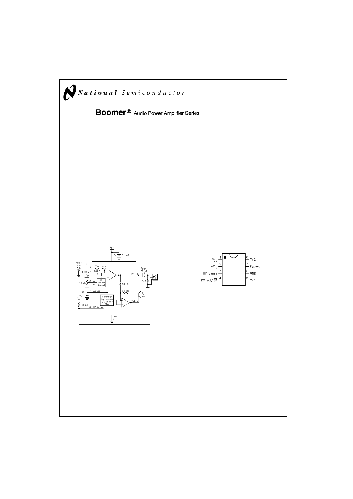
Typical Application Connection Diagram
BOOMER™is a trademark ofNational Semiconductor Corporation.
DS101025-1
FIGURE 1. Typical Audio Amplifier
Application Circuit
MSOP, SOP Package
DS101025-2
Top View
Order Number LM4865M, LM4865MM
See NS Package Number M08A, MUA08A
December 1999
LM4865 750 mW Audio Power Amplifier with DC Volume Control and Headphone Switch
© 1999 National Semiconductor Corporation DS101025 www.national.com
Page 2
Absolute Maximum Ratings (Note 2)
If Military/Aerospace specified devices are required,
please contact the National Semiconductor Sales Office/
Distributors for availability and specifications.
Supply Voltage 6.0V
Storage Temperature −65˚C to +150˚C
Input Voltage −0.3V to V
DD
+0.3V
Power Dissipation (Note 3) Internally Limited
ESD Susceptibility (Note 4) 2000V
ESD Susceptibility (Note 5) 200V
Junction Temperature 150˚C
Soldering Information
Vapor Phase (60 sec.) 215˚C
Infrared (15 sec.) 220˚C
Thermal Resistance
θ
JC
(SOP) 35˚C/W
θ
JA
(SOP) 150˚C/W
θ
JC
(MSOP) 56˚C/W
θ
JA
(MSOP) 190˚C/W
Operating Ratings
Temperature Range
T
MIN
≤ TA≤ T
MAX
−40˚C ≤ TA≤ +85˚C
Supply Voltage 2.7V ≤ V
DD
≤ 5.5V
See AN-450 “Surface Mounting and their Effects on Product
Reliability” for other methods of soldering surface mount
devices.
Electrical Characteristics (Notes 1, 2)
he following specifications apply for V
DD
=
5V, unless otherwise specified. Limits apply for T
A
=
25˚C.
Symbol Parameter Conditions
LM4865
Units
(Limits)
Typical
(Note 6)
Limit
(Note 7)
V
DD
Supply Voltage 2.7 V (min)
5.5 V (max)
I
DD
Quiescent Power Supply
Current
VIN= 0V, IO= 0A, HP Sense = 0V 4 7 mA (max)
V
IN
= 0V, IO- 0A, HP Sense = 5V 3.5 6 mA (max)
I
SD
Shutdown Current V
PIN4
≤ 0.3V 0.7 µA
V
OS
Output Offset Voltage VIN= 0V 5 50 mV (max)
P
O
Output Power THD = 1%(max), HP Sense<0.8V,f=1kHz,
R
L
=8Ω
750 500
mW
(max)
THD=10%(max), HP Sense
<
0.8V,
f = 1 kHz, R
L
=8Ω
1.0 W
THD+N=1%, HP Sense
>
4V,f=1kHz,
R
L
=32Ω
80 mW
THD=10%, HP Sense
>
4V,f=1kHz,
R
L
=32Ω
110 mW
THD+N Total Harmonic Distortion +
Noise
P
O
= 300 mWrms,f=20Hz–20kHz, RL=8Ω
0.6
%
PSSR Power Supply Rejection Ratio V
RIPPLE
= 200 mVrms, RL=8Ω,CB= 1.0 µF,
f=1kHz
50 dB
C
RANGE
Attenuator Range-Single Ended Gain with V
PIN4
≥ 4.0V, (80%of VDD) 20 18.8 dB (min)
Attenuation with V
PIN4
≤ 0.9V, (20%of VDD) −72 −70 dB (min)
V
IH
HP Sense High Input Voltage 4 V (max)
V
IL
HP Sense Low Input Voltage 0.8 V (min)
Note 1: All voltages are measured with respect to the ground pin, unless otherwise specified.
Note 2:
“Absolute Maximum Ratings”
indicate limits beyond which damage to the device may occur.
“Operating Ratings”
indicate conditions for which the device is
functional, but do not guarantee specific performance limits.
“Electrical Characteristics”
state DC andAC electrical specifications under particular test conditions which
guarantee specific performance limits. This assumes that the device is within the Operating Ratings. Specifications are not guaranteed for parameters where no limit
is given, however, the typical value is a good indication of device performance.
Note 3: The maximum power dissipation must be derated at elevated temperatures and is dictated by T
JMAX
, θJA, and the ambient temperature TA. The maximum
allowable power dissipation is P
DMAX
=
(T
JMAX−TA
)/θJAor the number given in the Absolute Maximum Ratings, whichever is lower. For the LM4865M, T
JMAX
=
150˚C.
Note 4: Human body model, 100 pF discharged through a 1.5 kΩ resistor.
Note 5: Machine Model, 220 pF–240 pF discharged through all pins.
Note 6: Typicals are measured at 25˚C and represent the parametric norm.
Note 7: Limits are guaranteed to National’s AOQL (Average Outgoing Quality Level).
Note 8: The quiescent power supply current depends on the offset voltage when a practical load is connected to the amplifier.
LM4865
www.national.com 2
Page 3
External Components Description
(
Figure 1
)
Components Functional Description
1. C
i
Input coupling capacitor which blocks the DC voltage at the amplifier’s input terminals. It also creates a
highpass filter with the internal R
i
. The designer should note that10kOhm<(Ri)<110kOhm.Therefore fc=
1/(2πR
iCi
). Refer to the section, Proper Selection of External Components, for an explanation of how to
determine the value of C
i
.
2. C
S
Supply bypass capacitor which provides power supply filtering. Refer to the Power Supply Bypassing
section for information concerning proper placement and selection of the supply bypass capacitor.
3. C
B
Bypass pin capacitor which provides half-supply filtering. Refer to the section, Proper Selection of
External Components, for information concerning proper placement and selection of C
B
.
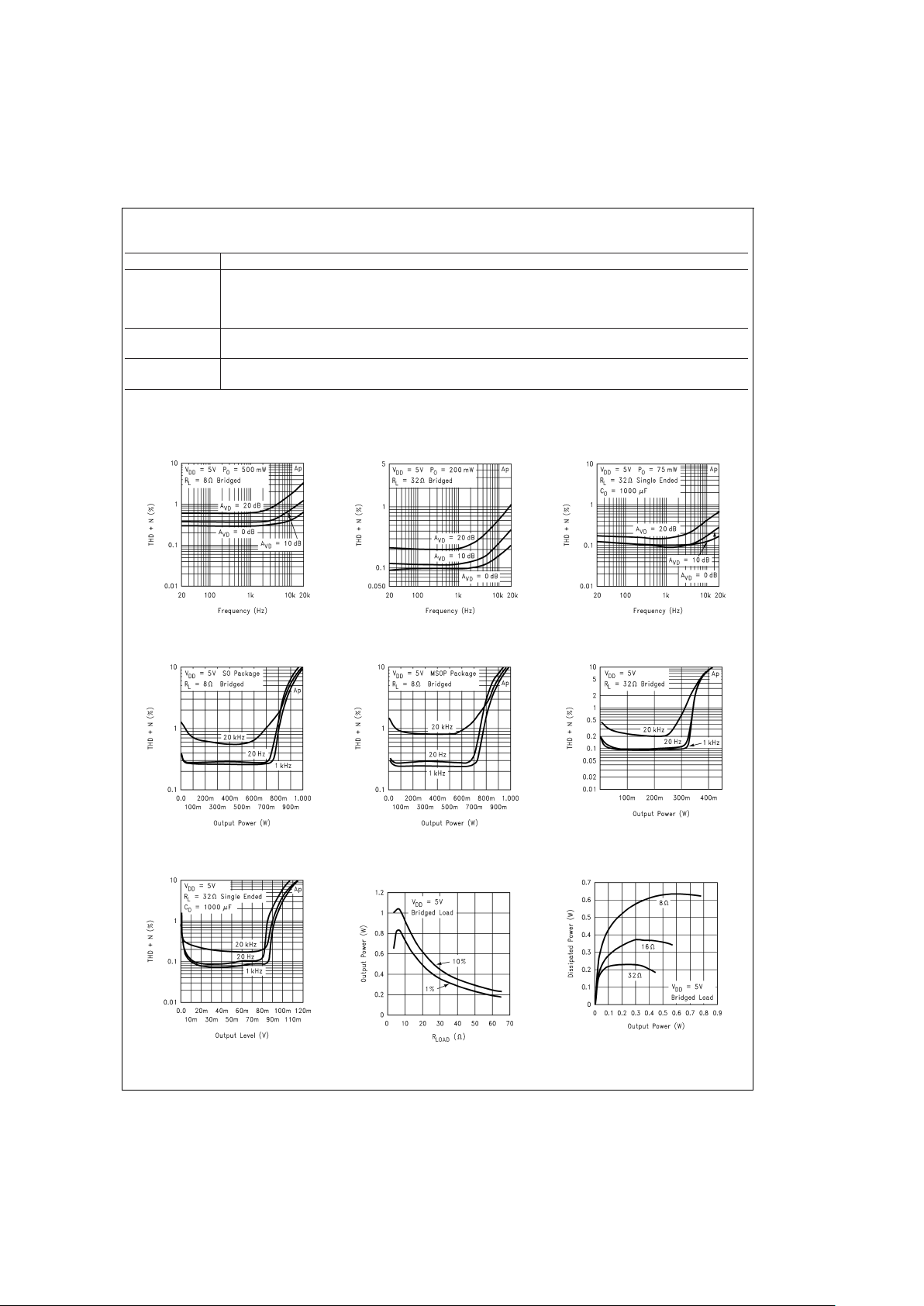
Typical Performance Characteristics
THD+N vs Frequency
DS101025-5
THD+N vs Frequency
DS101025-6
THD+N vs Output Power
DS101025-7
THD+N vs Output Power
DS101025-8
THD+N vs Output Power
DS101025-9
THD+N vs Output Power
DS101025-10
THD+N vs Output Power
DS101025-11
Power Dissipation vs Load
Resistance
DS101025-12
Power Dissipation vs Output Power
DS101025-13
LM4865
www.national.com3
Page 4

Typical Performance Characteristics (Continued)
Power Derating Curve
DS101025-14
Clipping Voltage vs RL
DS101025-15
Noise Floor
DS101025-16
Frequency Response vs
Input Capacitor Size
DS101025-17
Power Supply
Rejection Ratio
DS101025-18
Attenuation Level vs
DC-Vol Amplitude
DS101025-19
THD+N vs Frequency
DS101025-20
THD+N vs Frequency
DS101025-21
THD+N vs Frequency
DS101025-22
LM4865
www.national.com 4
Page 5

Typical Performance Characteristics (Continued)
Application Information
BRIDGE CONFIGURATION EXPLANATION
As shown in
Figure 1
, the LM4865 has two operational amplifiers internally, allowing for a few different amplifier configurations. The first amplifier’s gain is DC voltage controlled,
while the second amplifier is internally fixed in a unity-gain,
inverting configuration. The closed-loop gain of the first amplifier is set by an external DC voltage (refer to (
Figure 1
),
while the second amplifier’s gain is fixed by the two internal
20 kΩ resistors.
Figure 1
shows that the output of amplifier one serves as the
input to amplifier two which results in both amplifiers producing signals identical in magnitude, but out of phase 180˚.
By driving the load differentially through outputs V
O1
and
V
O2
, an amplifier configuration commonly referred to as
“bridged mode” is established. Bridged mode operation is
different from the classical single-ended amplifier configuration where one side of its load is connected to ground.
A bridge amplifier design has a few distinct advantages over
the single-ended configuration, as it provides differential
drive to the load, thus doubling output swing for a specified
supply voltage. Four times the output power is possible as
compared to a single-ended amplifier under the same conditions. This increase in attainable output assumes that the
amplifier is not current limited or clipped. In order to choose
an amplifier’s closed-loop gain without causing excessive
clipping, please refer to the Audio Power Amplifier Design
section.
THD+N vs Output Power
DS101025-23
THD+N vs Output Power
DS101025-24
THD+N vs Output Power
DS101025-28
Output Power vs Load Resistance
DS101025-29
Clipping Voltage vs Supply Voltage
DS101025-30
Output Power vs Supply Voltage
DS101025-31
Output Power vs Supply Voltage
DS101025-32
Supply Current vs Supply Voltage
DS101025-33
LM4865
www.national.com5
Page 6

Application Information (Continued)
A bridge configuration, such as the one used in LM4865,
also creates a second advantage over single-ended amplifiers. Since the differential outputs, V
O1
and VO2, are biased
at half-supply,no net DC voltage exists across the load. This
eliminates the need for an output coupling capacitor which is
required in a single supply,single-ended amplifier configuration. If an output coupling capacitor is not used in a
single-ended configuration, the half-supply bias across the
load would result in both increased internal IC power dissipation as well as permanent loudspeaker damage.
POWER DISSIPATION
Power dissipation is a major concern when designing a successful amplifier, whether the amplifier is bridged or
single-ended.
Equation (1)
states the maximum power dissipation point for a single-ended amplifier operating at a given
supply voltage and driving a specified output load.
P
DMAX
=
(V
DD
)2/(2π2RL) Single-Ended (1)
However, a direct consequence of the increased power delivered to the load by a bridge amplifier is an increase in internal power dissipation point for a bridge amplifier operating
at the same given conditions.
P
DMAX
=
4*(V
DD
)2/(2π2RL) Bridge Mode (2)
Since the LM4865 has two operational amplifiers in one
package, the maximum internal power dissipation is 4 times
that of a single-ended amplifier. Even with this substantial increase in power dissipation, the LM4865 does not require
heatsinking. From
Equation (1)
, assuming a 5V power supply and an 8Ω load, the maximum power dissipation point is
633 mW. The maximum power dissipation point obtained
from
Equation (2)
must not be greater than the power dissi-
pation that results from
Equation (3)
:
P
DMAX
=
(T
JMAX–TA
)/θ
JA
(3)
For package M08A, θ
JA
=
150˚C/W, and for package
MUA08A, θ
JA
=
190˚C/W. T
JMAX
=
150˚C for the LM4865.
Depending on the ambient temperature, T
A
, of the system
surroundings,
Equation (3)
can be used to find the maximum
internal power dissipation supported by the IC packaging. If
the result of
Equation (2)
is greater than that of
Equation (3)
,
then either the supply voltage must be decreased, the load
impedance increased, or the ambient temperature reduced.
For the typical application of a 5V power supply, with an 8Ω
load, the maximum temperature possible without violating
the maximum junction temperature is approximately 55˚C
provided that device operation is around the maximum
power dissipation point and assuming surface mount packaging. Internal power dissipation is a function of output
power. If typical operation is not around the maximum power
dissipation point, the ambient temperature can be increased.
Refer to the Typical Performance Characteristics curves
for power dissipation information for lower output powers.
POWER SUPPLY BYPASSING
As with any power amplifier,proper supply bypassing is critical for low noise performance and high power supply rejection. The capacitor location on both the bypass and power
supply pins should be as close to the device as possible. The
effect of a larger half supply bypass capacitor is improved
PSRR due to increased half-stability. Typical applications
employ a 5V regulator with 10 µF and a 0.1 µF bypass capacitors which aid in supply stability,but do not eliminate the
need for bypassing the supply nodes of the LM4865. The selection of bypass capacitors, especially C
B
, is thus depen-
dent upon desired PSRR requirements, click and pop performance as explained in the section, Proper Selection of
External Components, system cost, and size constraints.
SHUTDOWN FUNCTION
In order to reduce power consumption while not in use, the
LM4865 contains a DC Vol/SD pin. The DC Vol/SD pin allows the LM4865 to externally turn off the amplifier’s bias circuitry.The shutdown feature turns the amplifier off when the
DC Vol/SD pin is brought below 0.3 volts. When the DC
Vol/SD pin is between 0.3V to 0.5V, the LM4865 will be either be in shutdown or mute mode. In mute mode the current
drawn will be that of the quiescent supply current. The DC
Vol/SD pin should be tied to GND supply rail for best performance if the LM4865 is to go into shutdown mode.As the DC
Vol/SD is increased above 0.5V the amplifier will follow the
attenuation and gain curve in Typical Performance Charac-
teristics.
HP-Sense FUNCTION
The LM4865 possesses a headphone control pin that turns
off the amplifier which drives +Vo2 so that single-ended operation can occur and a bridged connected load is muted.
Quiescent current consumption is reduced when the IC is in
this single-ended mode.
Figure 2
shows the implementation of the LM4865’s headphone control function using a single-supply headphone amplifier. The voltage divider of R1 and R2 sets the voltage at
the HP-Sense pin (pin 3) to be approximately 50 mV when
there are no headphones plugged into the system. This
logic-low voltage at the HP-Sense pin enables the LM4865
and places it in bridged mode operation. The output coupling
capacitors protect the headphones by blocking the amplifier’s half supply DC voltage.
When there are no headphones plugged into the system and
the IC is in bridged mode configuration, both loads are essentially at a 0V DC potential. Since the HP-Sense threshold
is set at 4V,even in an ideal situation, the output swing cannot cause a false single-ended trigger.
When a set of headphones are plugged into the system, the
contact pin of the headphone jack is disconnected from the
signal pin, interrupting the voltage divider set up by resistors
R1 and R2. Resistor R1 then pulls up the HP-Sense pin, enabling the headphone function. This disables the second
side of the amplifier thus muting the bridged speakers. The
amplifier then drives the headphones, whose impedance is
in parallel with resistor R2. Resistor R2 has negligible effect
on output drive capability since the typical impedance of
headphones are 32Ω.
The LM4865 can be used to drive both a bridged 8Ω speaker
anda32Ωheadphone without using the HP-Sense pin. In
this case the HP-Sense would not be connected to the headphone jack but to a microprocessor or a switch. By enabling
the HP-Sense pin, the 8Ω speaker can be muted.
PROPER SELECTION OF EXTERNAL COMPONENTS
Proper selection of external components in applications using integrated power amplifiers is critical to optimize device
and system performance. While the LM4865 is tolerant to a
variety of external component combinations, consideration
to component values must be used to maximize overall system quality.
LM4865
www.national.com 6
Page 7

Application Information (Continued)
Selection of Input Capacitor Size
Large input capacitors are both expensive and space hungry
for portable designs. Clearly, a certain sized capacitor is
needed to couple in low frequencies without severe attenuation. But in many cases the speakers used in portable systems, whether internal or external, have little ability to reproduce signals below 150 Hz. In this case using a large input
capacitor may not increase system performance.
Besides minimizing the input capacitor size, careful consideration should be paid to the bypass capacitor value. Bypass
capacitor, C
B
, is the most critical compoment to minimize
turn-on pops since it determines how fast the LM4865 turns
on. The slower the LM4865’s outputs ramp to their quiescent
DC voltage (nominally 1/2 V
DD
), the smaller the turn-on pop.
Choosing C
B
equal to 1.0 µF along with a small value of C
i
(in the range of 0.1 µF to 0.39 µF), should produce a clickless and popless shutdown function.Pick C
i
as small as pos-
sible as to minimize clicks and pops.
Click And Pop Circuitry
The LM4865 contains circuitry to minimize turn-on and shutdown transients or “clicks and pops”. In this case, turn-on refers to either power supply turn-on or the device coming out
of shutdown mode. When the device is turning on, the amplifiers are internally configured as unity gain buffers. An internal current source ramps up the voltage of the bypass pin.
Both the inputs and outputs ideally track the voltage at the
bypass pin. The device will remain in buffer mode until the
bypass pin has reached its half supply voltage, 1/2 V
DD
.As
soon as the bypass node is stable, the device will become
fully operational, where the gain is set by the external voltage on the DC Vol/SD pin.
Although the bypass pin current source cannot be modified,
the size of C
B
can be changed to alter the device turn-on
time and the amount of “clicks and pops”. By increasing the
value of C
B
the amount of turn-on pop can be reduced. However,the tradeoff for using a larger bypass capacitor is an increase in turn-on time for this device. There is a linear relationship between the size of C
B
and the turn-on time. Here
are some typical turn-on times for a given C
B
:
C
B
T
ON
0.01 µF 20 ms
0.1 µF 200 ms
0.22 µF 420 ms
0.47 µF 840 ms
1.0 µF 2 Sec
In order eliminate “clicks and pops”, all capacitors must be
discharged before turn-on. Rapid switching of VDD may
cause the ″clicks and pops″ to be not easily controlled. In a
single-ended configuration, the output coupling capacitor, C
O
, is of particular concern. This capacitor discharges through
internal 20 kΩ resistors. Depending on the size of C
O
, the
time constant can be relatively large. To reduce transients in
single-ended mode, an external 1 kΩ–5 kΩ resistor can be
placed in parallel with the internal 20 kΩ resistor. The
tradeoff for using this resistor is an increase in quiescent current.
DS101025-34
FIGURE 2. Headphone Circuit
LM4865
www.national.com7
Page 8

Physical Dimensions inches (millimeters) unless otherwise noted
Order Number LM4865M
NS Package Number M08A
LM4865
www.national.com 8
Page 9

Physical Dimensions inches (millimeters) unless otherwise noted (Continued)
LIFE SUPPORT POLICY
NATIONAL’S PRODUCTS ARE NOT AUTHORIZED FOR USE AS CRITICAL COMPONENTS IN LIFE SUPPORT
DEVICES OR SYSTEMS WITHOUT THE EXPRESS WRITTEN APPROVAL OF THE PRESIDENT AND GENERAL
COUNSEL OF NATIONAL SEMICONDUCTOR CORPORATION. As used herein:
1. Life support devices or systems are devices or
systems which, (a) are intended for surgical implant
into the body, or (b) support or sustain life, and
whose failure to perform when properly used in
accordance with instructions for use provided in the
labeling, can be reasonably expected to result in a
significant injury to the user.
2. A critical component is any component of a life
support device or system whose failure to perform
can be reasonably expected to cause the failure of
the life support device or system, or to affect its
safety or effectiveness.
National Semiconductor
Corporation
Americas
Tel: 1-800-272-9959
Fax: 1-800-737-7018
Email: support@nsc.com
National Semiconductor
Europe
Fax: +49 (0) 1 80-530 85 86
Email: europe.support@nsc.com
Deutsch Tel: +49 (0) 1 80-530 85 85
English Tel: +49 (0) 1 80-532 78 32
Français Tel: +49 (0) 1 80-532 93 58
Italiano Tel: +49 (0) 1 80-534 16 80
National Semiconductor
Asia Pacific Customer
Response Group
Tel: 65-2544466
Fax: 65-2504466
Email: sea.support@nsc.com
National Semiconductor
Japan Ltd.
Tel: 81-3-5639-7560
Fax: 81-3-5639-7507
www.national.com
8-Lead (0.118’’ Wide) Molded Mini Small Outline Package
Order Number LM4865MM
NS Package Number MUA08A
LM4865 750 mW Audio Power Amplifier with DC Volume Control and Headphone Switch
National does not assume any responsibility for use of any circuitry described, no circuit patent licenses are implied and National reserves the right at any time without notice to change said circuitry and specifications.
 Loading...