

Page 1
LM4854
1.9W Monaural, 85mW Stereo Headphone Audio
Amplifier
General Description
The unity-gain stable LM4854 is both a mono differential
output (for bridge-tied loads, or BTL) audio power amplifier
and a single-ended (SE) stereo headphone amplifier. Operating on a single 5V supply, the mono BTL mode delivers
1.1W (typ) to an 8Ω load, 1.7W (typ) to a 4Ω load (Note 1) at
1% THD+N. In SE stereo mode, the amplifier will deliver
85mW to 32Ω loads. The LM4854 features a new circuit
topology that suppresses output transients (’click and pops’)
and eliminates SE-mode output coupling capacitors, saving
both component and board space costs. The LM4854 has
three inputs: one pair for a two-channel stereo signal and the
third for a single-channel mono input.
The LM4854 is designed for PDA, cellular telephone, notebook, and other handheld portable applications. It delivers
high quality output power from a surface-mount package and
requires few external components. Other features include an
active-low micropower shutdown mode, an "instant-on" low
power standby mode, and thermal shutdown protection.
The LM4854 is available in the very space-efficient 12-lead
micro SMD, exposed-DAP LLP for higher power applications, and TSSOP packages.
Note 1: An LM4854LD that has been properly mounted to a circuit board will
deliver 1.7W (typ) into a 4Ω load.
Key Specifications
j
LLP BTL output power (RL= 3.2Ω and
THD+N = 1%)
VDD= 3.0V 1.0W (typ)
V
DD
= 5.0V 1.9W (typ)
j
LLP BTL output power (RL=4Ω and
THD+N = 1%)
VDD= 3.0V 900mW (typ)
V
DD
= 5.0V 1.7W (typ)
j
LLP BTL output power (RL=8Ω and
THD+N = 1%)
VDD= 3.0V 380mW (typ)
V
DD
= 5.0V 1.1W (typ)
j
SE output power (RL=32Ω and THD+N
= 1.0%)
V
DD
= 3.0V 32mW (typ)
V
DD
= 5.0V 93mW (typ)
j
Micropower shutdown supply current
V
DD
= 3.0V 0.005µA (typ)
V
DD
= 5.0V 0.05µA (typ)
j
Standby supply current
V
DD
= 3.0V 16µA (typ)
V
DD
= 5.0V 27µA (typ)
j
PSRR (f = 1kHz, 3.0V ≤ VDD≤ 5.0V,
(Fig. 1))
BTL 60dB (typ)
SE 66dB (typ)
Features
n Fast 0.1ms (typ) and 1.0ms (max) turn-on and turn-off
time
n Eliminates SE amplifier output coupling capacitors
n Advanced "click and pop" suppression circuitry
n Stereo headphone amplifier mode
n Low-power standby and ultra-low current micropower
shutdown modes
n Thermal shutdown protection circuitry
n 2.4V to 5.5V operation
n Unity-gain stable
n Gain set with external resistors
n Space-saving micro SMD package, exposed-DAP LLP,
and TSSOP
Applications
n PDAs
n Notebook computers
n Cellular phones
n Handheld portable electronic devices
Boomer®is a registered trademark of National Semiconductor Corporation.
April 2003
LM4854 1.9W Monaural, 85mW Stereo Headphone Audio Amplifier
© 2003 National Semiconductor Corporation DS200382 www.national.com
Page 2
Typical Application
(Pin out shown for the 12-pin large bump micro SMD IBL package. Consult the "Connection Diagrams" for the LLP or MT
package pin out.)
20038201
FIGURE 1. Typical Audio Amplifier Application Circuit
LM4854
www.national.com 2
Page 3
Connection Diagrams
20038202
Top View (Bump-side down)
Order Number LM4854IBL
See NS Package Number BLA12BAB
Micro SMD Marking
20038203
Top View
X - Date Code
T - Die Traceability
G - Boomer Family
54 - LM4854IBL
LM4854IBL Pin Designation
Pin (Bump) Number Pin Function
A1 L-IN
B1 GND
C1 R-IN
D1 MONO-IN
A2 L-OUT
B2 BYPASS
C2 HP-SENSE
D2 R-OUT
A3 SHUTDOWN
B3 V
DD
C3 BTL-OUT
D3 STANDBY
LM4854
www.national.com3
Page 4
Connection Diagrams
20038204
Top View
Order Number LM4854LD
See NS Package Number LDA14A
200382A5
Top View
U - Fab Code
Z - Plant Code
XY - Date Code
TT - Die Tracebility
Bottom Line - Part Number
20038205
Top View
Order Number LM4854MT
See NS Package Number MTC14
200382A6
Top View
Z - Plant Code
XY - Date Code
TT - Die Traceability
Bottom 2 lines - Part Number
LM4854
www.national.com 4
Page 5
Absolute Maximum Ratings (Notes 2,
3)
If Military/Aerospace specified devices are required,
please contact the National Semiconductor Sales Office/
Distributors for availability and specifications.
Supply Voltage 6.0V
Storage Temperature −65˚C to +150˚C
Input Voltage −0.3V to V
DD
+ 0.3V
Power Dissipation(Note 4) Internally Limited
ESD Susceptibility (Note 5)
All pins except Pin C3 (IBL), Pin11
(LD/MT) 2000V
Pin C3 (IBL), Pin 11 (LD/MT) 8000V
ESD Susceptibility(Note 6) 200V
Junction Temperature (T
J
) 150˚C
Solder Information
Small Outline Package
Vapor Phase (60 sec.) 215˚C
Infrared (15 sec.) 220˚C
See AN-540 "Surface Mounting and
their Effects on Product Reliability"
for other methods of soldering
surface-mount devices.
Thermal Resistance
θ
JA
(typ) — BLA12BAB 121˚C/W
θ
JC
(typ) — LDA14A 3˚C/W
θ
JA
(typ) — LDA14A 42˚C/W (Note 7)
θ
JC
(typ) — MTC14 40˚C/W
θ
JA
(typ) — MTC14 109˚C/W
Operating Ratings (Note 3)
Temperature Range
T
MIN
≤ TA≤ T
MAX
−40˚C ≤ TA≤ +85˚C
Supply Voltage 2.4V ≤ V
DD
≤ 5.5V
Electrical Characteristics for Entire Amplifier (VDD= 5V)
The following specifications apply for circuit shown in Figure 1, unless otherwise specified. Limits apply for TA= 25˚C.
Symbol Parameter Conditions LM4854 Units
(Limits)
Typical
(Note 8)
Limit
(Notes 9,
10)
I
DD
Quiescent Power Supply Current VIN= 0V; IO= 0A, No Load 5.0 12 mA max)
V
IN
= 0V; IO= 0A, 8Ω Load 6.5 15 mA (max)
I
STBY
Standby Quiescent Power Supply
Current
V
STANDBY
= GND 27 35 µA (max)
I
SD
Shutdown Quiescent Power
Supply Current
V
SHUTDOWN
= GND 0.05 0.2 µA (max)
V
OS
Output Offset Voltage 8Ω Load 2.0 40 mV (max)
PSRR Power Supply Rejection Ratio C
BYPASS
= 1.0µF, R
SOURCE
=10Ω
V
RIPPLE
= 200mV
p-p
sinewave
BTL, R
L
=8Ω,RIN=10Ω
f
IN
= 217Hz
f
IN
= 1kHz
SE, R
L
=32Ω,RIN=10Ω
f
IN
= 217Hz
f
IN
= 1kHz
61
63
dB
dB
68
71
dB
dB
t
RSH
Return-from-Shutdown Time C
BYPASS
= 1.0µF 200 ms
t
RST
Return-from-Standby Time 0.1 1.0 ms(max)
V
IH
Shutdown or Standby Logic High
Treshold
1.4 V (min)
V
IL
Shutdown or Standby Logic Low
Treshold
0.4 V (max)
LM4854
www.national.com5
Page 6
Electrical Characteristics Bridged-Mode Operation (VDD= 5V)
The following specifications apply for for the circuit shown in Figure 1 and a measurement bandwith of 20Hz to 80kHz, unless
otherwise specified. Limits apply for T
A
= 25˚C.
Symbol Parameter Conditions LM4854 Units
(Limits)
Typical
(Note 8)
Limit
(Notes 9,
10)
P
O
Output Power (Note 11) THD = 1% (max); f = 1kHz (Note12)
R
L
= 3.2Ω (LM4854LD)
R
L
=4Ω (LM4854LD)
R
L
=8Ω
1.9
1.7
1.1 1.0
W
W
W (min)
THD = 10% (max); f = 1kHz (Note12)
R
L
= 3.2Ω (LM4854LD)
R
L
=4Ω (LM4854LD)
R
L
=8Ω
2.3
2.1
1.3
W
W
W
THD+N Total Harmonic Distortion+Noise 20Hz ≤ f
IN
≤ 20kHz
R
L
=4Ω,PO= 1.0W (LM4854LD)
R
L
=8Ω,PO= 400mW
0.3
0.18
%
%
f
IN
= 1kHz
R
L
=4Ω,PO= 1.5W (LM4854LD)
R
L
=8Ω,PO= 50mW
0.1
0.08
%
%
S/N Signal-to-Noise Ratio f
IN
= 1kHz, C
BYPASS
= 1.0µF
P
O
= 900mW, RL=8Ω 90 dB
Electrical Characteristics : SE Operation (VDD= 5V)
The following specifications apply for for the circuit shown in Figure 1 and a measurement bandwith of 20Hz to 80kHz, unless
otherwise specified. Limits apply for T
A
= 25˚C.
Symbol Parameter Conditions LM4854 Units
(Limits)
Typical
(Note 8)
Limit
(Notes 9,
10)
P
O
Output Power (Note 11) THD+N = 1.0%, f = 1kHz, RL=32Ω
THD+N = 10%, f = 1kHz, R
L
=32Ω
THD+N = 1.0%, f = 1kHz, R
L
=16Ω
THD+N = 10%, f = 1kHz, R
L
=16Ω
93
105
170
200
85
140
mW(min)
mW
mW(min)
mW
THD+N Total Harmonic Distortion+Noise 20Hz ≤ f
IN
≤ 20kHz
R
L
=32Ω,PO= 50mW 0.3 %
VOUT Output Voltage Swing THD = 1.0%, R
L
=5kΩ 4.0 V
P-P
XTALK Channel Separation fIN= 1kHz, C
BYPASS
= 1.0µF, RL=32Ω 55 dB
S/N Signal-to-Noise Ratio f
IN
= 1kHz, C
BYPASS
= 1.0µF
P
O
= 50mW, RL=32Ω 90 dB
Electrical Characteristics for Entire Amplifier (VDD= 3.0V)
The following specifications apply for circuit shown in Figure 1, unless otherwise specified. Limits apply for TA= 25˚C.
Symbol Parameter Conditions LM4854 Units
(Limits)
Typical
(Note 8)
Limit
(Notes 9,
10)
I
DD
Quiescent Power Supply Current VIN= 0V, IO= 0A, 8Ω Load 4.0 10 mA (max)
I
STBY
Standby Quiescent Power Supply
Current
V
STANDBY
= GND 16.0 20.0 µA (max)
I
SD
Shutdown Current V
SHUTDOWN
= GND 0.005 0.02 µA (max)
V
OS
Output Offset Voltage 8 Ω Load 2.0 40 mV (max)
LM4854
www.national.com 6
Page 7
Electrical Characteristics for Entire Amplifier (VDD= 3.0V) (Continued)
The following specifications apply for circuit shown in Figure 1, unless otherwise specified. Limits apply for TA= 25˚C.
Symbol Parameter Conditions LM4854 Units
(Limits)
Typical
(Note 8)
Limit
(Notes 9,
10)
PSRR Power Supply Rejection Ratio C
BYPASS
= 1.0µF, R
SOURCE
=10Ω
V
RIPPLE
= 200mV
p-p
sinewave
BTL, R
L
=8Ω,RIN=10Ω
f
IN
= 217Hz
f
IN
= 1kHz
SE, R
L
=32Ω,RIN=10Ω
f
IN
= 217Hz
f
IN
= 1kHz
62
62
dB
dB
68
72
dB
dB
t
RSH
Return-from-Shutdown Time C
BYPASS
= 1.0µF 200 ms
t
RST
Return-from-Standby Time 0.1 1.0 ms(max)
V
IH
Shutdown or Standby Logic High
Treshold
1.4 V (min)
V
IL
Shutdown or Standby Logic Low
Treshold
0.4 V (max)
Electrical Characteristics : Bridged-Mode Operation (VDD= 3.0V) (Notes 4, 9)
The following specifications apply for for the circuit shown in Figure 1 and a measurement bandwith of 20Hz to 80kHz, unless
otherwise specified. Limits apply for T
A
= 25˚C.
Symbol Parameter Conditions LM4854 Units
(Limits)
Typical
(Note 8)
Limit
(Notes 9,
10)
P
O
Output Power (Note11) THD = 1% (max); f = 1kHz (Note11)
R
L
=4Ω (LM4854LD)
R
L
=8Ω
1.0
380 350
W
mW (min)
THD = 10% (max); f = 1kHz (Note11)
RL=4Ω (LM4854LD)
R
L
=8Ω
1.1
530
W
mW
THD+N Total Harmonic Distortion+Noise 20Hz ≤ f
IN
≤ 20kHz
R
L
=4Ω,PO= 800mW (LM4854LD)
R
L
=8Ω,PO= 150mW
0.3
0.21
%
%
f
IN
= 1kHz
R
L
=4Ω,PO= 500mW (LM4854LD)
R
L
=8Ω,PO= 150mW
0.1
0.075
%
%
S/N Signal-to-Noise Ratio f
IN
= 1kHz, C
BYPASS
= 1.0µF
P
O
= 900mW, RL=8Ω 90 dB
LM4854
www.national.com7
Page 8
Electrical Characteristics : SE Operation (VDD= 3.0V) (Notes 4, 9)
The following specifications apply for for the circuit shown in Figure 1 and a measurement bandwith of 20Hz to 80kHz, unless
otherwise specified. Limits apply for T
A
= 25˚C.
Symbol Parameter Conditions LM4854 Units
(Limits)
Typical
(Note 8)
Limit
(Notes 9,
10)
P
O
Output Power (Note 11) THD+N = 1.0%, f = 1kHz, RL=32Ω
THD+N = 10%, f = 1kHz, R
L
=32Ω
THD+N = 1.0%, f = 1kHz, R
L
=16Ω
THD+N = 10%, f = 1kHz, R
L
=16Ω
32
60
57
100
27
38
mW(min)
mW
mW (min)
mW
THD+N Total Harmonic Distortion+Noise 20Hz ≤ f
IN
= ≤ 20kHz
R
L
=32Ω,PO= 30mW 0.3 %
VOUT Output Voltage Swing THD = 0.5%, R
L
=5kΩ 2.4 V
P-P
XTALK Channel Separation fIN= 1kHz, C
BYPASS
= 1.0µF, RL=32Ω 55 dB
S/N Signal-to-Noise Ratio f
IN
= 1kHz, C
BYPASS
= 1.0µF
P
O
= 30mW, RL=32Ω
TBD dB
Note 2: All voltages are measured with respect to the GND pin unless other wise specified.
Note 3: Absolute Maximum Ratings indicate limits beyond which damage to the device may occur. Operating Ratings indicate conditions for which the device is
functional but do not guarantee specific performance limits. Electrical Characteristics state DC and AC electrical specifications under particular test conditions that
guarantee specific performance limits. This assumes that the device is within the Operating Ratings. Specifications are not guaranteed for parameters where no limit
is given, however, the typical value is a good indication of device performance.
Note 4: The maximum power dissipation must be derated at elevated temperatures and is dictated by T
JMAX
, θJA, and the ambient temperature, TA. The maximum
allowable power dissipation is P
DMAX
=(T
JMAX-TA
)/θJAor the number given in Absolute Maximum Ratings, whichever is lower. For the LM4854, see power derating
currents for more information.
Note 5: Human body model, 100pF discharged through a 1.5kΩ resistor.
Note 6: Machine Model, 220pF-240pF discharged through all pins.
Note 7: The given θ
JA
is for an LM4854 packaged in an LDA14A with the Exposed-DAP soldered to an exposed 2in2 area of 1oz printed circuit board copper.
Note 8: Typicals are measured at 25˚C and represent the parametric norm.
Note 9: Limits are guaranteed to National’s AOQL (Average Outgoing Quality Level).
Note 10: Datasheet minimum and maximum specification limits are guaranteed by design, test, or statistical analysis.
Note 11: Output power is measured at the amplifier’s package pins.
Note 12: When driving 4Ω loads and operating on a 5V supply, the LM4854LD must be mounted to a circuit board that has a minimum of 2.5in2 of exposed,
uninterrupted copper area connected to the LLP package’s exposed DAP.
LM4854
www.national.com 8
Page 9
External Components Description
See Figure 1.
Components Functional Description
1. R
i
This is the inverting input resistance that, along with Rf, sets the closed-loop gain. Input resistance Riand
input capacitance C
i
form a high pass filter. The filter’s cutoff frequency is fc= 1/2πRiCi.
2. C
i
This is the input coupling capacitor. It blocks DC voltage at the amplifier’s inverting input. Ciand Ricreate a
highpass filter. The filter’s cutoff frequency is f
c
= 1/2πRiCi. Refer to the Application Information section,
SELECTING EXTERNAL COMPONENTS, for an explanation of determining C
i
’s value.
3. R
f
This is the feedback resistance that, along with Ri, sets the closed-loop gain.
4. C
s
The supply bypass capacitor. Refer to the POWER SUPPLY BYPASSING section for information about
properly placing, and selecting the value of, this capacitor.
5. C
B
This capacitor filters the half-supply voltage present on the BYPASS pin. Refer to the Application
Information section, SELECTING EXTERNAL COMPONENTS, for information about properly placing, and
selecting the value of, this capacitor..
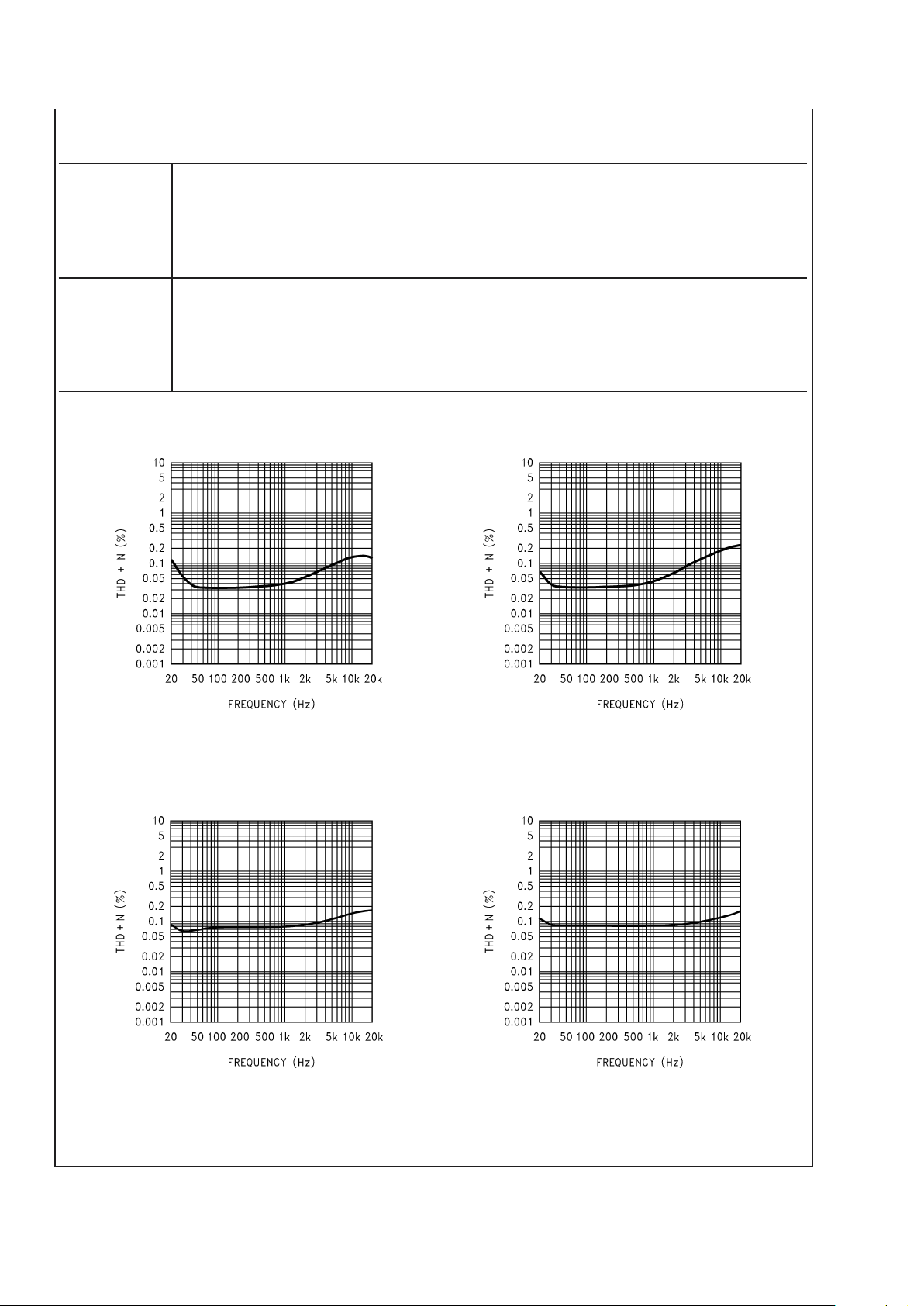
Typical Performance Characteristics
THD+N vs Frequency THD+N vs Frequency
200382D8
LM4854LD
V
DD
= 5V, RL=4Ω (BTL),
P
OUT
= 1000mW
200382D9
LM4854LD
V
DD
= 5V, RL=4Ω (BTL),
P
OUT
= 400mW
THD+N vs Frequency THD+N vs Frequency
200382C0
VDD= 5V, RL=8Ω (BTL),
P
OUT
= 400mW
200382B8
VDD= 5V, RL=16Ω (SE),
P
OUT
= 50mW
LM4854
www.national.com9
Page 10

Typical Performance Characteristics (Continued)
THD+N vs Frequency THD+N vs Frequency
200382B9
VDD= 5V, RL=32Ω (SE),
P
OUT
= 50mW
200382E0
LM4854LD
V
DD
= 3V, RL=4Ω (BTL),
P
OUT
= 150mW
THD+N vs Frequency THD+N vs Frequency
200382B7
VDD= 3V, RL=8Ω (BTL),
P
OUT
= 150mW
200382B5
VDD= 3V, RL=16Ω (SE),
P
OUT
= 30mW
LM4854
www.national.com 10
Page 11

Typical Performance Characteristics (Continued)
THD+N vs Frequency THD+N vs Output Power
200382B6
VDD= 3V, RL=32Ω (SE),
P
OUT
= 30mW
200382E1
LM4854LD
V
DD
= 5V, RL=4Ω (BTL),
at (from top to bottom at 200mW)
20kHZ, 20Hz, 1kHz
THD+N vs Output Power THD+N vs Output Power
200382C6
VDD= 5V, RL=8Ω (BTL),
at (from top to bottom at 0.2W)
20kHz, 20Hz, 1kHz
200382C4
VDD= 5V, RL=16Ω (SE),
at (from top to bottom at 30mW)
20kHz, 20Hz, 1kHz
LM4854
www.national.com11
Page 12

Typical Performance Characteristics (Continued)
THD+N vs Output Power THD+N vs Output Power
200382C5
VDD= 5V, RL=32Ω (SE),
at (from top to bottom at 20mW)
20kHz, 20Hz, 1kHz
200382E2
LM4854LD
V
DD
= 3V, RL=4Ω (BTL),
at (from top to bottom at 200mW)
20kHz, 20Hz, 1kHz
THD+N vs Output Power
THD+N vs Output Power
200382C3
VDD= 3V, RL=8Ω (BTL),
at (from top to bottom at 0.02W)
20kHz, 20Hz, 1kHz
200382C1
VDD= 3V, RL=16Ω (SE),
at (from top to bottom at 20mW)
20kHz, 20Hz, 1kHz
LM4854
www.national.com 12
Page 13

Typical Performance Characteristics (Continued)
THD+N vs Output Power Output Power
vs Power Supply Voltage
200382C2
VDD= 3V, RL=32Ω (SE),
at (from top to bottom at 20mW)
20kHz, 20Hz, 1kHz
200382A8
RL=8Ω (BTL), fIN= 1kHz,
at (from top to bottom at 4V)
10% THD+N, 1% THD+N
Output Power
vs Power Supply Voltage
PSRR vs Frequency
200382A7
RL=16Ω (BTL), fIN= 1kHz,
at (from top to bottom at 4V):
10% THD+N, 1% THD+N
200382E3
LM4854LD
V
DD
= 5V, RL=4Ω (BTL),
R
SOURCE
=10Ω
LM4854
www.national.com13
Page 14

Typical Performance Characteristics (Continued)
PSRR vs Frequency PSRR vs Frequency
200382B4
VDD= 5V, RL=8Ω (BTL),
R
SOURCE
=10Ω
200382B2
VDD= 5V, RL=16Ω (SE),
R
SOURCE
=10Ω
PSRR vs Frequency PSRR vs Frequency
200382B3
VDD= 5V, RL=32Ω (SE),
R
SOURCE
=10Ω
200382E4
LM4854LD
V
DD
= 3V, RL=4Ω (BTL),
R
SOURCE
=10Ω
LM4854
www.national.com 14
Page 15

Typical Performance Characteristics (Continued)
PSRR vs Frequency PSRR vs Frequency
200382B1
VDD= 3V, RL=8Ω (BTL),
R
SOURCE
=10Ω
200382A9
VDD= 3V, RL=16Ω (SE),
R
SOURCE
=10Ω
PSRR vs Frequency Amplifier Power Dissipation
vs Load Power Dissipation
200382B0
VDD= 3V, RL=32Ω (SE),
R
SOURCE
=10Ω
200382D1
LM4854IBL/MT, VDD= 5V,
R
L
=8Ω (BTL), fIN= 1kHz
LM4854
www.national.com15
Page 16

Typical Performance Characteristics (Continued)
Amplifier Power Dissipation
vs Load Power Dissipation
Amplifier Power Dissipation
vs Load Power Dissipation
200382C7
LM4854IBL/MT, VDD= 5V,
(from top to bottom at 0.04W):
R
L
=16Ω (SE), RL=32Ω (SE), fIN= 1kHz,
both channels driven and loaded
200382C8
LM4854IBL/MT, VDD= 3V,
R
L
=8Ω (BTL), fIN= 1kHz
Power Dissipation
Derating Curves
Power Dissipation
Derating Curve
200382E9
LM4854LD, VDD= 5V,
R
L
=8Ω (BTL), fIN= 1kHz,
(from top to bottom at 120˚C):
4in
2
copper plane heatsink area
1in
2
copper plane heatsink area
200382E6
LM4854IBL, VDD= 5V,
R
L
=8Ω (BTL), fIN= 1kHz
LM4854
www.national.com 16
Page 17

Typical Performance Characteristics (Continued)
Power Dissipation
Derating Curve
Amplifier Power Dissipation
vs Load Power Dissipation
200382E7
LM4854MT, VDD= 5V,
R
L
=8Ω (BTL), fIN= 1kHz
200382C9
LM4854IBL/MT, VDD= 3V,
(from top to bottom at 0.02W):
R
L
=16Ω (SE), RL=32Ω (SE), fIN= 1kHz,
both channels driven and loaded
Output Power
vs Load Resistance
Output Power
vs Load Resistance
200382D2
LM4854IBL/MT, BTL Load,
(from top to bottom at 12Ω):
V
DD
= 5V, THD+N = 10%;
V
DD
= 5V, THD+N = 1%
V
DD
= 3V, THD+N = 10%
V
DD
= 3V, THD+N = 1%
200382D3
LM4854IBL/MT, SE Load (both channels driven and
loaded),
f
IN
= 1kHz, (from top to bottom at 12Ω):
V
DD
= 5V, THD+N = 10%;
V
DD
= 5V, THD+N = 1%
V
DD
= 3V, THD+N = 10%
V
DD
= 3V, THD+N = 1%
LM4854
www.national.com17
Page 18

Typical Performance Characteristics (Continued)
Channel-to-Channel Crosstalk
vs Frequency
Channel-to-Channel Crosstalk
vs Frequency
200382D4
VDD= 5V, RL=16Ω (SE)
A = Left channel driven, right channel measured
B = Right channel driven, left channel measured
200382D5
VDD= 5V, RL=32Ω (SE)
A = Left channel driven, right channel measured
B = Right channel driven, left channel measured
Channel-to-Channel Crosstalk
vs Frequency
Channel-to-Channel Crosstalk
vs Frequency
200382D6
VDD= 3V, RL=16Ω (SE)
A = Left channel driven, right channel measured
B = Right channel driven, left channel measured
200382D7
VDD= 3V, RL=32Ω (SE)
A = Left channel driven, right channel measured
B = Right channel driven, left channel measured
Application Information
ELIMINATING OUTPUT COUPLING CAPACITORS
Typical single-supply audio amplifiers that can switch between driving bridge-tied-load (BTL) speakers and singleended (SE) headphones use a coupling capacitor on each
SE output. This capacitor blocks the half-supply voltage to
which the output amplifiers are typically biased and couples
the audio signal to the headphones. The signal returns to
circuit ground through the headphone jack’s sleeve.
The LM4854 eliminates these coupling capacitors. When the
LM4854 is configured to drive SE loads, AMP2 is internally
configured to apply V
DD
/2 to a stereo headphone jack’s
sleeve. This voltage equals the quiescent voltage present on
the Amp1 and Amp3 outputs that drive the headphones.
Headphones driven by the LM4854 operate in a manner very
similar to a BTL load. The same DC voltage is applied to
each input terminal on a headphone speaker. This results in
no net DC current flow through the speaker. AC current flows
through a headphone speaker as an audio signal’s output
amplitude increases on one of the speaker’s terminal.
When operating as a headphone amplifier, the headphone
jack sleeve is not connected to circuit ground, but to V
DD
/2.
Using the headphone output jack as a line-level output will
place the LM4854’s one-half supply voltage on a plug’s
sleeve connection. Driving a portable notebook computer or
audio-visual display equipment is possible. This presents no
difficulty when the external equipment uses capacitively
coupled inputs. For the very small minority of equipment that
is DC-coupled, the LM4854 monitors the current supplied by
LM4854
www.national.com 18
Page 19

Application Information (Continued)
the amplifier that drives the headphone jack’s sleeve. If this
current exceeds 500mA
PK
, the amplifier is shutdown, pro-
tecting the LM4854 and the external equipment. For more
information, see the section titled ’Single-Ended Output
Power Performance and Measurement Considerations’.
EXPOSED-DAP MOUNTING CONSIDERATIONS
The LM4854’s exposed-DAP (die attach paddle) package
(LD) provides a low thermal resistance between the die and
the PCB to which the part is mounted and soldered. This
allows rapid heat transfer from the die to the surrounding
PCB copper area heatsink, copper traces, ground plane, and
finally, surrounding air. The result is a low voltage audio
power amplifier that produces 1.7W dissipation in a 4Ω load
at ≤ 1% THD+N and over 1.9W in a 3Ω load at 10% THD+N.
This high power is achieved through careful consideration of
necessary thermal design. Failing to optimize thermal design
may compromise the LM4854’s high power performance and
activate unwanted, though necessary, thermal shutdown
protection.
The LD package must have its DAP soldered to a copper
pad on the PCB. The DAP’s PCB copper pad is then, ideally,
connected to a large plane of continuous unbroken copper.
This plane forms a thermal mass, heat sink, and radiation
area. Place the heat sink area on either outside plane in the
case of a two-sided or multi-layer PCB. (The heat sink area
can also be placed on an inner layer of a multi-layer board.
The thermal resistance, however, will be higher.) Connect
the DAP copper pad to the inner layer or backside copper
heat sink area with 6 (3 X 2) (LD) vias. The via diameter
should be 0.012in - 0.013in with a 1.27mm pitch. Ensure
efficient thermal conductivity by plugging and tenting the vias
with plating and solder mask, respectively.
Best thermal performance is achieved with the largest practical copper heat sink area. If the heatsink and amplifier
share the same PCB layer, a nominal 2.5in
2
(min) area is
necessary for 5V operation with a 4Ω load. Heatsink areas
not placed on the same PCB layer as the LM4854 should be
5in
2
(min) for the same supply voltage and load resistance.
The last two area recommendations apply for 25˚C ambient
temperature. Increase the area to compensate for ambient
temperatures above 25˚C. In all circumstances and under all
conditions, the junction temperature must be held below
150˚C to prevent activating the LM4854’s thermal shutdown
protection. The LM4854’s power de-rating curve in the Typi-
cal Performance Characteristics shows the maximum
power dissipation versus temperature. Example PCB layouts
for the exposed-DAP TSSOP and LD packages are shown in
the Demonstration Board Layout section. Further detailed
and specific information concerning PCB layout and fabrication and mounting an LD (LLP) is found in National Semiconductor’s AN1187.
20038207
FIGURE 2. Typical Audio Amplifier Application Circuit
LM4854
www.national.com19
Page 20

Application Information (Continued)
PCB LAYOUT AND SUPPLY REGULATION
CONSIDERATIONS FOR DRIVING 3Ω AND 4Ω LOADS
Power dissipated by a load is a function of the voltage swing
across the load and the load’s impedance. As load impedance decreases, load dissipation becomes increasingly dependent on the interconnect (PCB trace and wire) resistance
between the amplifier output pins and the load’s connections. Residual trace resistance causes a voltage drop,
which results in power dissipated in the trace and not in the
load as desired. For example, 0.1Ω trace resistance reduces
the output power dissipated by a 4Ω load from 1.7W to 1.6W.
The problem of decreased load dissipation is exacerbated
as load impedance decreases. Therefore, to maintain the
highest load dissipation and widest output voltage swing,
PCB traces that connect the output pins to a load must be as
wide as possible.
Poor power supply regulation adversely affects maximum
output power. A poorly regulated supply’s output voltage
decreases with increasing load current. Reduced supply
voltage causes decreased headroom, output signal clipping,
and reduced output power. Even with tightly regulated supplies, trace resistance creates the same effects as poor
supply regulation. Therefore, making the power supply
traces as wide as possible helps maintain full output voltage
swing.
BRIDGE CONFIGURATION EXPLANATION
As shown in Figure 2, the LM4854 consists of three operational amplifiers. In mono mode, AMP1 and AMP2 operate in
series to drive a speaker connected between their outputs.
In stereo mode, AMP1 and AMP3 are used to drive stereo
headphones or other SE load.
In mono mode, external resistors R
fL
and RiLset the closedloop gain of AMP1, whereas two internal 20kΩ resistors set
AMP2’s gain at -1. The LM4854 drives a load, such as a
speaker, connected between the two amplifier outputs,
L-OUT and BTL-OUT.
Figure 2 shows that AMP1’s output serves as AMP2’s input.
This results in both amplifiers producing signals identical in
magnitude, but 180˚ out of phase. Taking advantage of this
phase difference, a load is placed between L-OUT and BTLOUT and driven differentially (commonly referred to as
"bridge mode"). This results in a differential,or BTL, gain of:
A
VD
= 2(Rf/Ri) (1)
Bridge mode amplifiers are different from single-ended amplifiers that drive loads connected between a single amplifier’s output and ground. For a given supply voltage, bridge
mode has a distinct advantage over the single-ended configuration: its differential output doubles the voltage swing
across the load. Theoretically, this produces four times the
output power when compared to a single-ended amplifier
under the same conditions. This increase in attainable output
power assumes that the amplifier is not current limited and
that the output signal is not clipped. To ensure minimum
output signal clipping when choosing an amplifier’s closedloop gain, refer to the Audio Power Amplifier Design section.
Another advantage of the differential bridge output is no net
DC voltage across the load. This is accomplished by biasing
AMP1’s and AMP2’s outputs at half-supply. This eliminates
the coupling capacitor that single supply, single-ended amplifiers require. Eliminating an output coupling capacitor in a
typical single-ended configuration forces a single-supply amplifier’s half-supply bias voltage across the load. This increases internal IC power dissipation and may permanently
damage loads such as speakers.
POWER DISSIPATION
Power dissipation is a major concern when designing a
successful single-ended or bridged amplifier. Equation (2)
states the maximum power dissipation point for a singleended amplifier operating at a given supply voltage and
driving a specified output load.
P
DMAX-SE
=(VDD)2/(2π2RL): Single-Ended (2)
However, a direct consequence of the increased power delivered to the load by a bridge amplifier is higher internal
power dissipation for the same conditions. The LM4854 has
two operational amplifiers driving a mono bridge load. The
maximum internal power dissipation operating in the bridge
mode is twice that of a single-ended amplifier. From Equation (3), assuming a 5V power supply and an 8Ω load, the
maximum BTL-mode power dissipation is 317mW.
P
DMAX-MONOBTL
= 4(VDD)2/(2π2RL): Bridge Mode (3)
The maximum power dissipation point given by Equation (3)
must not exceed the power dissipation given by Equation
(4):
P
DMAX
’=(T
JMAX-TA
)/ θ
JA
(4)
The LM4854’s TJMAX = 150˚C. In the IBL package, the
LM4854’s θ
JA
is 121˚C/W. The LM4854’s T
JMAX
= 150˚C. In
the LD package soldered to a DAP pad that expands to a
copper area of 2.0in
2
on a PCB, the LM4854’s θJAis 42˚C/W.
In the MT package, the LM4854’s θ
JA
is 109˚C/W. At any
given ambient temperature T
A
, use Equation (4) to find the
maximum internal power dissipation supported by the IC
packaging. Rearranging Equation (4) and substituting P
DMAX
for P
DMAX
’ results in Equation (5). This equation gives the
maximum ambient temperature that still allows maximum
stereo power dissipation without violating the LM4854’s
maximum junction temperature.
T
A=TJMAX-PDMAX-MONOBTLθJA
(5)
For a typical application with a 5V power supply and an 8Ω
load, the maximum ambient temperature that allows maximum stereo power dissipation without exceeding the maximum junction temperature is approximately 73˚C for the IBL
package.
T
JMAX=PDMAX-MONOBTLθJA+TA
(6)
Equation (6) gives the maximum junction temperature T
J
-
MAX
. If the result violates the LM4854’s 150˚C, reduce the
maximum junction temperature by reducing the power supply voltage or increasing the load resistance. Further allowance should be made for increased ambient temperatures.
The above examples assume that a device is a surface
mount part operating around the maximum power dissipation
point. Since internal power dissipation is a function of output
LM4854
www.national.com 20
Page 21

Application Information (Continued)
power, higher ambient temperatures are allowed as output
power or duty cycle decreases. If the result of Equation (3) is
greater than that of Equation (4), then decrease the supply
voltage, increase the load impedance, or reduce the ambient
temperature. If these measures are insufficient, a heat sink
can be added to reduce θ
JA
. The heat sink can be created
using additional copper area around the package, with connections to the ground pin(s), supply pin and amplifier output
pins. External, solder attached SMT heatsinks such as the
Thermalloy 7106D can also improve power dissipation.
When adding a heat sink, the θ
JA
is the sum of θJC, θCS, and
θ
SA
.(θJCis the junction-to-case thermal impedance, θCSis
the case-to-sink thermal impedance, and θ
SA
is the sink-toambient thermal impedance.) Refer to the Typical Performance Characteristics curves for power dissipation information at lower output power levels.
POWER SUPPLY BYPASSING
As with any power amplifier, proper supply bypassing is
critical for low noise performance and high power supply
rejection. Applications that employ a 5V regulator typically
use a 10µF in parallel with a 0.1µF filter capacitors to stabilize the regulator’s output, reduce noise on the supply line,
and improve the supply’s transient response. However, their
presence does not eliminate the need for a local 1.0µF
tantalum bypass capacitance connected between the
LM4854’s supply pins and ground. Do not substitute a ceramic capacitor for the tantalum. Doing so may cause oscillation. Keep the length of leads and traces that connect
capacitors between the LM4854’s power supply pin and
ground as short as possible. Connecting a 1µF capacitor,
CB, between the BYPASS pin and ground improves the
internal bias voltage’s stability and improves the amplifier’s
PSRR. The PSRR improvements increase as the bypass pin
capacitor value increases. Too large, however, increases
turn-on time and can compromise the amplifier’s click and
pop performance. The selection of bypass capacitor values,
especially CB, depends on desired PSRR requirements,
click and pop performance (as explained in the section,
Proper Selection of External Components), system cost, and
size constraints.
STANDBY
The LM4854 features a low-power, fast turn-on standby
mode. Applying a logic-low to the STANDBY pin act actives
the standby mode. When this mode is active, the power
supply current decreases to a nominal value of 30µA and the
amplifier outputs are muted. Fast turn-on is assured because all bias points remain at the same voltage as when the
part is in fully active operation. The LM4854 returns to fully
active operation in 100µs (typ) after the input voltage on the
STANDBY pin switches from a logic low to a logic high.
MICRO-POWER SHUTDOWN
The LM4854 features an active-low micro-power shutdown
mode. When active, the LM4854’s micro-power shutdown
feature turns off the amplifier’s bias circuitry, reducing the
supply current. The logic threshold is typically V
DD
/2. The
low 0.1µA typical shutdown current is achieved by applying a
voltage to the SHUTDOWN pin that is as near to GND as
possible. A voltage that is greater than GND may increase
the shutdown current.
CONTROLLING STANDBY AND MICROPOWER SHUTDOWN
There are a few methods to control standby or micro-power
shutdown. These include using a single-pole, single-throw
switch (SPST), a microprocessor, or a microcontroller. When
using a switch, connect a 100kΩ pull-up resistor between the
STANDBY or SHUTDOWN pin and V
DD
and the SPST
switch between the STANDBY or SHUTDOWN pin and
GND. Select normal amplifier operation by opening the
switch. Closing the switch applies GND to the STANDBY or
SHUTDOWN pins, activating micro-power shutdown. The
switch and resistor guarantee that the STANDBY or SHUTDOWN pins will not float. This prevents unwanted state
changes. In a system with a microprocessor or a microcontroller, use a digital output to apply the active-state voltage to
the STANDBY or SHUTDOWN pin.
HEADPHONE (SINGLE-ENDED) AMPLIFIER OPERATION
Previous single-supply amplifiers that were designed to drive
both BTL and SE loads used a SE (or headphone) "sense"
input. This input typically required two external resistors to
bias the sense input to a preset voltage that selected BTL
operation.
The LM4854 has a unique headphone sense circuit that
eliminates the external resistors. The amplifier has an internal comparator that monitors the voltage present on the
R-OUT pin. It compares this voltage against the voltage on
the HP-SENSE pin. When these voltages are equal, BTL
mode is selected and AMP3 is shutdown and its output has
a very high impedance. When the comparator’s input signals
are different, (a typical ∆V of 200mV), the comparator’s
output switches and activates the SE (headphone) mode.
AMP3 changes from shutdown state to an active state and,
along with AMP1, drives a stereo load. AMP2 drives the
headphone jack sleeve.
Figure 3 shows the suggested headphone jack electrical
connections. The jack is designed to mate with a three-wire
plug. The plug’s tip should carry a stereo signal’s leftchannel information. The ring adjacent to the tip should each
carry the right-channel signal and the ring furthest from the
tip provides the return to AMP2. A switch can replace the
headphone jack contact pin. When the switch shorts the
HP-SENSE pin to R-OUT, the bridge-connected speaker is
driven by AMP1 and AMP2. AMP3 is shutdown, its output in
a high-impedance state. When the switch opens, the
LM4854 operates in SE stereo mode. If headphone drive is
not needed, short the HP-SENSE pin to the R-OUT pin.
The LM4854’s unique headphone sense circuit requires a
dual switch headphone jack. A five-terminal headphone jack,
such as the Switchcraft 35RAPC4BH3, is shown in Figure 2.
For applications that require an SPDIF interface in the stereo
headphone jack, use a Foxconn 2F1138-TJ-TR.
LM4854
www.national.com21
Page 22

Application Information (Continued)
Figure 4 shows an optional resistor connected between the
amplifier output that drives the headphone jack sleeve and
ground. This resistor provides a ground path that supressed
power supply hum. This hum may occur in applications such
as notebook computers in a shutdown condition and connected to an external powered speaker. The resistor’s 100Ω
value is a suggested starting point. Its final value must be
determined based on the tradeoff between the amount of
noise suppression that may be needed and minimizing the
additional current drawn by the resistor (25mA for a 100Ω
resistor and a 5V supply).
Single-Ended Output Power Performance and Measurement Considerations
The LM4854 delivers clean, low distortion SE output power
into loads that are greater than 10Ω. As an example, output
power for 16Ω and 32Ω loads are shown in the Typical
Performance Characteristic curves. For loads less than 10Ω,
the LM4854 can typically supply 180mW of low distortion
power. However, when higher dissipation is desired in loads
less than 10Ω, a dramatic increase in THD+N may occur.
This is normal operation and does not indicate that proper
functionality has ceased. When a jump from moderate to
excessively high distortion is seen, simply reducing the output voltage swing will restore the clean, low distortion SE
operation.
The dramatic jump in distortion for loads less than 10Ω
occurs when current limiting circuitry activates. During SE
operation, AMP2 (refer to Figure 2) drives the headphone
sleeve. An on-board circuit monitors this amplifier’s output
current. The sudden increase in THD+N is caused by the
current limit circuitry forcing AMP2 into a high-impedance
output mode. When this occurs, the output waveform has
discontinuities that produce large amounts of distortion. It
has been observed that as the output power is steadily
increased, the distortion may jump from 5% to greater than
35%. Indeed, 10% THD+N may not actually be achievable.
ESD Protection
As stated in the Absolute Maximum Ratings, the AMP2
output pin has a maximum ESD susceptibility rating of
8000V. For higher ESD voltages, the addition of a PCDN042
dual transil (from California Micro Devices), as shown in
Figure 4, will provide additional protection.
SELECTING EXTERNAL COMPONENTS
Input Capacitor Value Selection
Amplifying the lowest audio frequencies requires high value
input coupling capacitor (Ci in Figure 2). A high value capacitor can be expensive and may compromise space efficiency
in portable designs. In many cases, however, the speakers
used in portable systems, whether internal or external, have
little ability to reproduce signals below 150Hz. Applications
using speakers with this limited frequency response reap
little improvement by using large input capacitor.
The LM4854’s advanced output transient suppression circuitry has eliminated the need to select the input capacitor’s
value in relation to the BYPASS capacitor’s value as was
necessary in some previous Boomer amplifiers. The value of
CI is now strictly determined by the desired low frequency
response.
As shown in Figure 2, the input resistor (R
i
) and the input
capacitor (C
i
) produce a high pass filter cutoff frequency that
is found using Equation (7).
f
c
=1/(2πRiCi) (7)
As an example when using a speaker with a low frequency
limit of 150Hz, C
i
, using Equation (7) is 0.063µF. The 1.0µF
C
i
shown in Figure 2 allows the LM4854 to drive high efficiency, full range speaker whose response extends below
30Hz.
Bypass Capacitor Value Selection
Besides minimizing the input capacitor size, careful consideration should be paid to value of CB, the capacitor connected to the BYPASS pin. Since C
B
determines how fast
the LM4854 settles to quiescent operation, its value is critical
when minimizing turn-on pops. The slower the LM4854’s
outputs ramp to their quiescent DC voltage (nominally V
DD
/
2), the smaller the turn-on pop. Choosing C
B
equal to 1.0µF
along with a small value of Ci (in the range of 0.1µF to
0.39µF), produces a click-less and pop-less shutdown function. As discussed above, choosing C
i
no larger than necessary for the desired bandwidth helps minimize clicks and
pops. CB’s value should be in the range of 5 times to 7 times
the value of C
i
. This ensures that output transients are
eliminated when power is first applied or the LM4854 resumes operation after shutdown.
20038212
FIGURE 3. Headphone Circuit
200382E8
FIGURE 4. The PCDN042 provides additional ESD
protection beyond the 8000V shown in the Absolute
Maximum Ratings for the AMP2 output
LM4854
www.national.com 22
Page 23

Application Information (Continued)
OPTIMIZING CLICK AND POP REDUCTION PERFORMANCE
The LM4854 contains circuitry that eliminates turn-on and
shutdown transients ("clicks and pops") and transients that
could occur when switching between BTL speakers and
single-ended headphones. For this discussion, turn-on refers to either applying the power supply voltage or when the
micro-power shutdown mode is deactivated.
As the V
DD
/2 voltage present at the BYPASS pin ramps to its
final value, the LM4854’s internal amplifiers are configured
as unity gain buffers and are disconnected from the L-OUT,
BTL-OUT, and R-OUT pins. An internal current source
charges the capacitor connected between the BYPASS pin
and GND in a controlled, linear manner. Ideally, the input and
outputs track the voltage applied to the BYPASS pin. The
gain of the internal amplifiers remains unity until the voltage
on the bypass pin reaches V
DD
/2. Once the voltage on the
bypass pin is stable and after a fixed nominal delay of
120ms, the device becomes fully operational and the amplifier outputs are reconnected to their respective output pins.
Although the BYPASS pin current cannot be modified,
changing the size of CB alters the device’s turn-on time.
There is a linear relationship between the size of CB and the
turn-on time. Here are some typical turn-on times for various
values of CB:
CB(µF) TON(ms)
0.01 120
0.1 130
0.22 140
0.47 160
1.0 200
2.2 300
In order eliminate "clicks and pops", all capacitors must be
discharged before turn-on. Rapidly switching V
DD
may not
allow the capacitors to fully discharge, which may cause
"clicks and pops".
AUDIO POWER AMPLIFIER DESIGN
Audio Amplifier Design: Driving 1W into an 8Ω Load
The following are the desired operational parameters:
•
Power Output: 1W
RMS
•
Load Impedance 8Ω
•
Input Level: 1V
RMS
•
Input Impedance: 20kΩ
•
Bandwidth: 100Hz - 20kHz±0.25dB
The design begins by specifying the minimum supply voltage
necessary to obtain the specified output power. One way to
find the minimum supply voltage is to use the Output Power
vs Supply Voltage curve in the Typical Performance Characteristics section. Another way, using Equation (8), is to calculate the peak output voltage necessary to achieve the
desired output power for a given load impedance. To account for the amplifier’s dropout voltage, two additional voltages, based on the Dropout Voltage vs Supply Voltage in the
Typical Performance Characteristics curves, must be added
to the result obtained by Equation (8). The result is Equation
(9).
(8)
V
DD=VOUTPEAK
+V
ODTOP+VODBOT
(9)
The Output Power vs. Supply Voltage graph for an 8Ω load
indicates a minimum supply voltage of 4.6V. The commonly
used 5V supply voltage easily meets this. The additional
voltage creates the benefit of headroom, allowing the
LM4854 to produce peak output power in excess of 1W
without clipping or other audible distortion. The choice of
supply voltage must also not create a situation that violates
of maximum power dissipation as explained above in the
Power Dissipation section. After satisfying the LM4854’s
power dissipation requirements, the minimum differential
gain needed to achieve 1W dissipation in an 8Ω load is
found using Equation (10).
(10)
Thus, a minimum gain of 2.83 allows the LM4854’s to reach
full output swing and maintain low noise and THD+N performance. For this example, let AVD = 3. The amplifier’s overall
gain is set using the input (R
i
) and feedback (Rf) resistors.
With the desired input impedance set at 20kΩ, the feedback
resistor is found using Equation (11).
R
f/Ri=AVD
/ 2 (11)
The value of R
f
is 30kΩ. The nominal output power is 1.13W.
TThe last step in this design example is setting the amplifier’s -3dB frequency bandwidth. To achieve the desired
±
0.25dB pass band magnitude variation limit, the low frequency response must extend to at least one-fifth the lower
bandwidth limit and the high frequency response must extend to at least five times the upper bandwidth limit. The gain
variation for both response limits is 0.17dB, well within the
±
0.25dB-desired limit. The results are an
f
L
= 100Hz / 5 = 20Hz (12)
and an
f
L
= 20kHz x 5 = 100kHz (13)
As mentioned in the SELECTING EXTERNAL COMPONENTS section, R
i
and Cicreate a highpass filter that sets
the amplifier’s lower bandpass frequency limit. Find the coupling capacitor’s value using Equation (14).
C
i
=1/(2πRifL) (14)
The result is
1/(2π x 20kΩ x 20Hz) = 0.397µF (15)
Use a 0.39µF capacitor, the closest standard value.
LM4854
www.national.com23
Page 24

Application Information (Continued)
The product of the desired high frequency cutoff (100kHz in
this example) and the differential gain AVD, determines the
upper passband response limit. With AVD = 3 and fH =
100kHz, the closed-loop gain bandwidth product (GBWP) is
300kHz. This is less than the LM4854’s 3.5MHz GBWP. With
this margin, the amplifier can be used in designs that require
more differential gain while avoiding performance restricting
bandwidth limitations.
RECOMMENDED PRINTED CIRCUIT BOARD LAYOUT
Figures 5 through 9 show the recommended four-layer PC
board layout that is optimized for the micro SMD-packaged
LM4854 and associated external components. Figures 10
through 12 show the recommended two-layer PC board
layout that is optimized for the TSSOP-packaged LM4854
and associated external components. Figures 13 through 17
show the recommended four-layer PC board layout that is
optimized for the LLP-packaged LM4854 and associate external components.
These circuits are designed for use with an external 5V
supply and 8Ω(min) speakers.These circuit boards are easy
to use. Apply 5V and ground to the board’s V
DD
and GND
pads, respectively. Connect a speaker between the board’s
L-OUT and BTL-OUT or headphones to the headphone jack
(L-OUT and R-OUT outputs).
Demonstration Board Layout
20038221
FIGURE 5. Recommended microSMD PC Board
Layout:
Component-Side SilkScreen
20038222
FIGURE 6. Recommended microSMD PC Board
Layout:
Component-Side Layout
20038223
FIGURE 7. Recommended microSMD PC Board
Layout:
Upper Inner-Layer Layout
20038224
FIGURE 8. Recommended microSMD PC Board
Layout:
Lower Inner-Layout Layer
LM4854
www.national.com 24
Page 25

Demonstration Board Layout
(Continued)
20038225
FIGURE 9. Recommended MM PC Board Layout:
Bottom_Side Layout
20038226
FIGURE 10. Recommended MT PC Board Layout:
Component-Side SilkScreen
20038227
FIGURE 11. Recommended MT PC Board Layout:
Component-Side Layout
20038228
FIGURE 12. Recommended MT PC Board Layout:
Bottom-Side Layout
20038229
FIGURE 13. Recommended LD PC Board Layout:
Component-Side SilkScreen
20038230
FIGURE 14. Recommended LD PC Board Layout:
Component-Side Layout
LM4854
www.national.com25
Page 26

Demonstration Board Layout (Continued)
20038231
FIGURE 15. Recommended LD PC Board Layout:
Upper Inner-Layer Layout
20038232
FIGURE 16. Recommended LD PC Board Layout:
Lower Inner-Layer Layout
20038233
FIGURE 17. Recommended LD PC Board Layout:
Bottom-Side Layout
LM4854
www.national.com 26
Page 27

Physical Dimensions inches (millimeters) unless otherwise noted
TSSOP Package
Order Number LM4854MT
NS Package Number MTC14
LM4854
www.national.com27
Page 28

Physical Dimensions inches (millimeters) unless otherwise noted (Continued)
14-Lead LLP Package
Order Number LM4854LD
NS Package Number LDA14A
LM4854
www.national.com 28
Page 29

Physical Dimensions inches (millimeters) unless otherwise noted (Continued)
12-Bump micro SMD Package
Order Number LM4854IBL, LM4854IBLX
NS Package Number BLA12BAB
X1 = 1.539
±
0.03 X2 = 1.996±0.03 X3 = 0.945±0.10
LIFE SUPPORT POLICY
NATIONAL’S PRODUCTS ARE NOT AUTHORIZED FOR USE AS CRITICAL COMPONENTS IN LIFE SUPPORT
DEVICES OR SYSTEMS WITHOUT THE EXPRESS WRITTEN APPROVAL OF THE PRESIDENT AND GENERAL
COUNSEL OF NATIONAL SEMICONDUCTOR CORPORATION. As used herein:
1. Life support devices or systems are devices or
systems which, (a) are intended for surgical implant
into the body, or (b) support or sustain life, and
whose failure to perform when properly used in
accordance with instructions for use provided in the
labeling, can be reasonably expected to result in a
significant injury to the user.
2. A critical component is any component of a life
support device or system whose failure to perform
can be reasonably expected to cause the failure of
the life support device or system, or to affect its
safety or effectiveness.
National Semiconductor
Americas Customer
Support Center
Email: new.feedback@nsc.com
Tel: 1-800-272-9959
National Semiconductor
Europe Customer Support Center
Fax: +49 (0) 180-530 85 86
Email: europe.support@nsc.com
Deutsch Tel: +49 (0) 69 9508 6208
English Tel: +44 (0) 870 24 0 2171
Français Tel: +33 (0) 1 41 91 8790
National Semiconductor
Asia Pacific Customer
Support Center
Fax: +65-6250 4466
Email: ap.support@nsc.com
Tel: +65-6254 4466
National Semiconductor
Japan Customer Support Center
Fax: 81-3-5639-7507
Email: jpn.feedback@nsc.com
Tel: 81-3-5639-7560
www.national.com
LM4854 1.9W Monaural, 85mW Stereo Headphone Audio Amplifier
National does not assume any responsibility for use of any circuitry described, no circuit patent licenses are implied and National reserves the right at any time without notice to change said circuitry and specifications.
 Loading...