

Page 1
LM4851
Integrated Audio Amplifier System
General Description
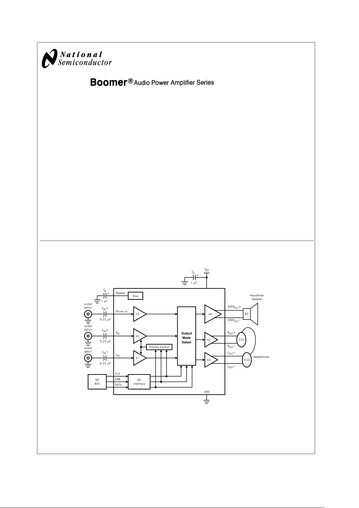
The LM4851 is an audio power amplifier system capable of
delivering 1.1W (typ) of continuous average power into a
mono 8Ω bridged-tied load (BTL) with 1% THD+N and
115mW (typ) per channel of continuous average power into
stereo 32Ω BTL loads with 0.5% THD+N, using a 5V power
supply.
The LM4851 features a 32 step digital volume control and
eight distinct output modes. The digital volume control and
output modes are programmed through a three-wire SPI
serial control interface, that allows flexibility in routing and
mixing audio channels. The LM4851 has 3 inputs: one pair
for a two-channel stereo signal and the third for a singlechannel mono input.
The LM4851 is designed for cellular phone, PDA, and other
portable handheld applications. It delivers high quality output
power from a surface-mount package and requires only five
external components.
The industry leading micro SMD package utilizes only 2mm
x 2.3mm of PCB space, making the LM4851 the most space
efficient audio sub system available today.
Key Specifications
n THD+N at 1kHz, 1.5W into 4Ω BTL (LQ) 1% (typ)
n THD+N at 1kHz, 1.1W into 8Ω BTL 1% (typ)
n THD+N at 1kHz, 115mW into 32Ω BTL 0.5% (typ)
n Single Supply Operation 2.6 to 5.0V
Features
n Mono 1.1W (typ) and stereo 115mW (typ) output
n SPI programmable 32 step digital volume control
(-40.5dB to +6dB)
n Eight distinct SPI programmable output modes
n micro-SMD and LLP surface mount packaging
n “Click and pop” suppression circuitry
n Thermal shutdown protection
n Low shutdown current (0.1µA, typ)
Applications
n Mobile phones
n PDAs
Typical Application
Boomer®is a registered trademark of National Semiconductor Corporation.
20040831
FIGURE 1. Typical Audio Amplifier Application Circuit
December 2002
LM4851 Integrated Audio Amplifier System
© 2002 National Semiconductor Corporation DS200408 www.national.com
Page 2
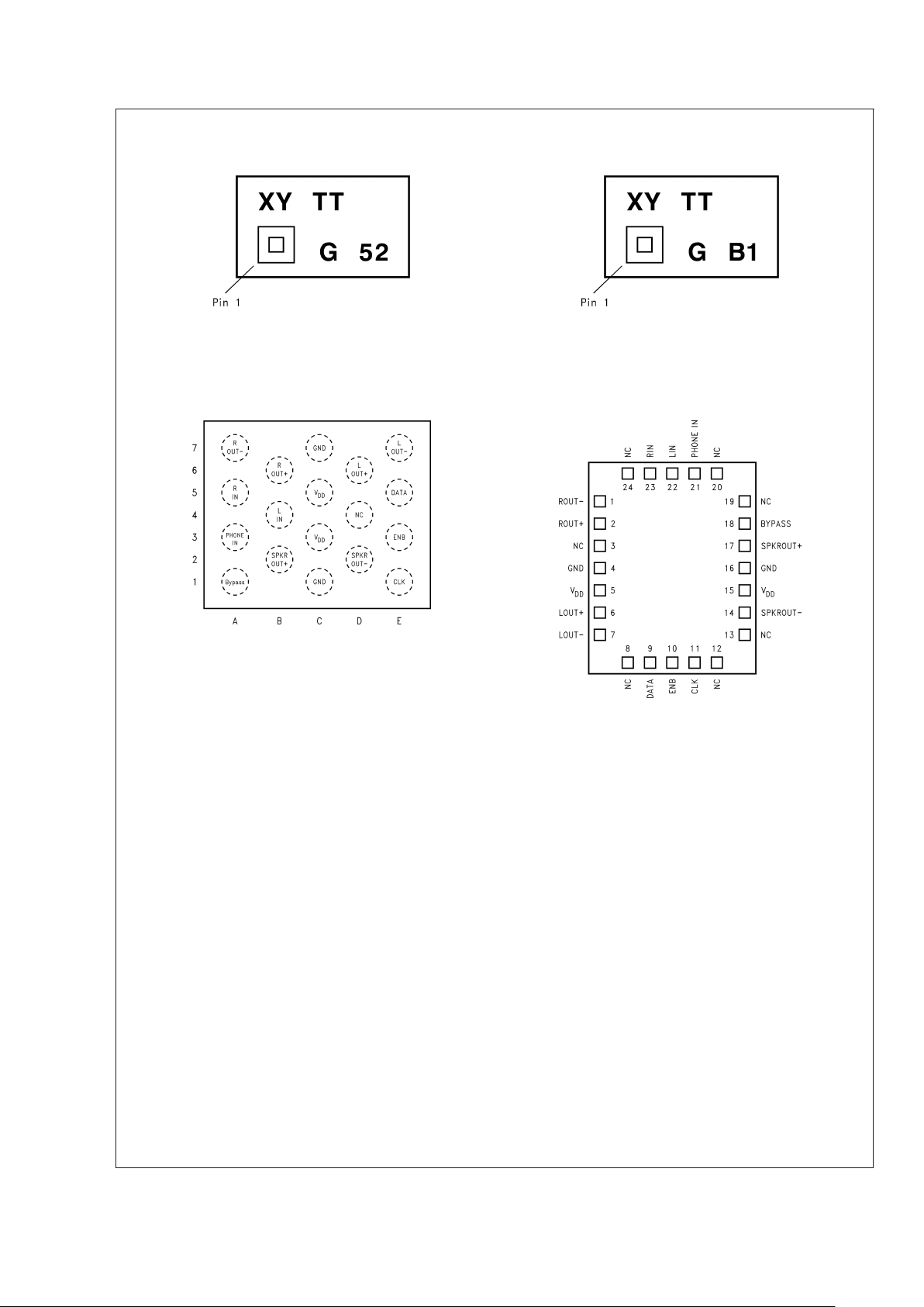
Connection Diagrams
18-Bump micro SMD Marking (IBL) 18-Bump micro SMD Marking (ITL)
200408A5
Top View
XY- Date Code
TT - Die Traceability
G - Boomer Family
52 - LM4851IBL-1
200408B3
Top View
XY- Date Code
TT - Die Traceability
G - Boomer Family
B1 - LM4851ITL
20040829
NC = NO CONNECT
Top View
(Bump-side down)
Order Number LM4851ITL, LM4851IBL
See NS Package Number TLA18AAA, BLA18AAB
200408A7
Top View
Order Number LM4851LQ
See NS Package Number LQA24A for Exposed-DAP LLP
LM4851
www.national.com 2
Page 3
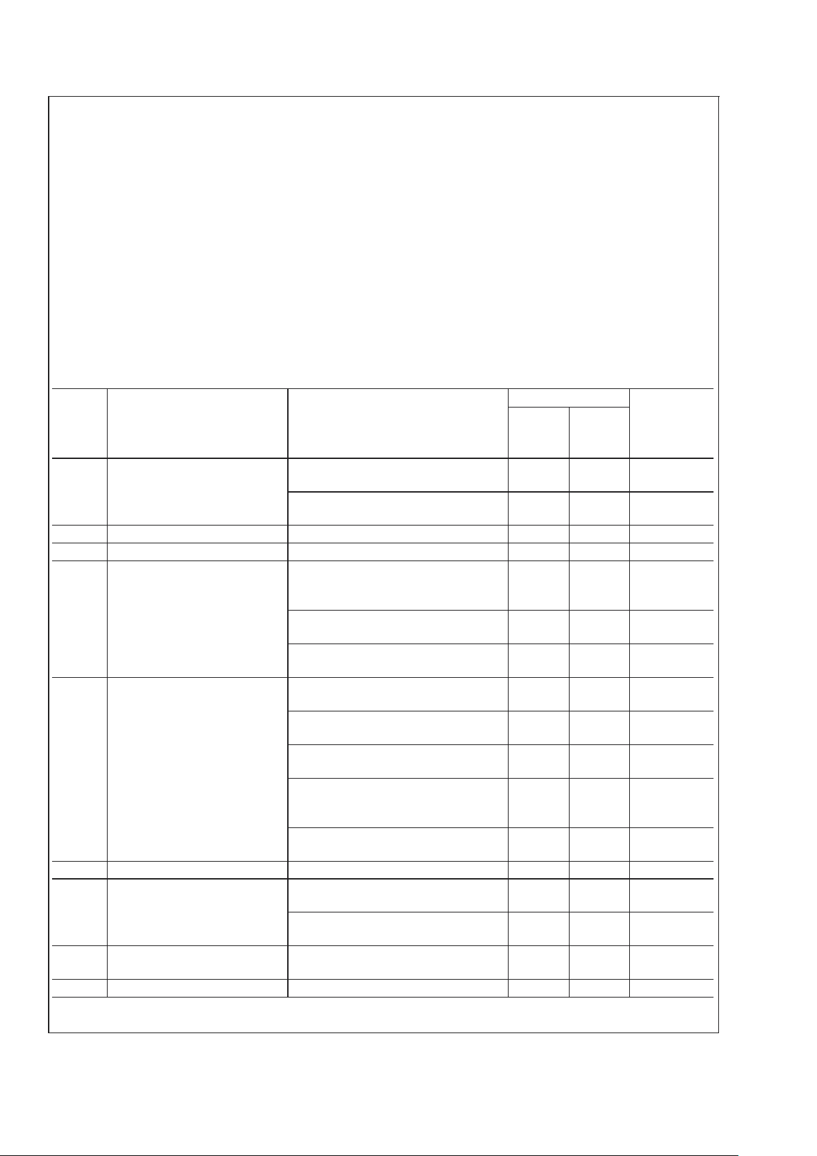
Absolute Maximum Ratings (Note 2)
If Military/Aerospace specified devices are required,
please contact the National Semiconductor Sales Office/
Distributors for availability and specifications.
Supply Voltage 6.0V
Storage Temperature −65˚C to +150˚C
ESD Susceptibility (Note 4) 2.0kV
ESD Machine model (Note 7) 200V
Junction Temperature (T
J
) 150˚C
Solder Information (Note 1)
Vapor Phase (60 sec.) 215˚C
Infrared (15 sec.) 220˚C
Thermal Resistance
θ
JA
(typ) - LQA24A 42˚C/W
θ
JC
(typ) - LQA24A 3.0˚C/W
θ
JA
(typ) - BLA18AAB 48˚C/W (Note 9)
θ
JC
(typ) - BLA18AAB 23˚C/W (Note 9)
θ
JA
(typ) - TLA18AAA 48˚C/W (Note 9)
θ
JC
(typ) - TLA18AAA 23˚C/W (Note 9)
Operating Ratings (Note 3)
Temperature Range −40˚C to 85˚C
Supply Voltage V
DD
2.6V ≤ VDD≤ 5.0V
Note 1: See AN-450 "Surface Mounting and their effects on Product Reliability" for other methods of soldering surface mount devices.
Electrical Characteristics (Notes 2, 8)
The following specifications apply for VDD= 5.0V, TA= 25˚C unless otherwise specified.
Symbol Parameter Conditions LM4851 Units
(Limits)
Typical
(Note 5)
Limit
(Note 6)
I
DD
Supply Current
Output mode 7
V
IN
= 0V; IO=0A
7.5 14 mA (max)
Output modes 1, 2, 3, 4, 5, 6
V
IN
= 0V; IO=0A
5.0 9.0 mA (max)
I
DD
Shutdown Current Output mode 0 0.1 2 µA (max)
V
OS
Output Offset Voltage VIN= 0V 5.0 50 mV (max)
P
O
Output Power
SPKR
OUT;RL
=4Ω
THD+N = 1%; f = 1kHz
LM4851LQ
1.5 W
SPKR
OUT;RL
=8Ω
THD+N = 1%; f = 1kHz
1.1 0.8 W (min)
R
OUT
and L
OUT;RL
=32Ω
THD+N = 0.5%; f = 1kHz
115 80 mW (min)
THD+N
Total Harmonic Distortion Plus
Noise
R
OUT
and L
OUT
; f = 1kHz
P
OUT
= 80mW; RL=32Ω
0.5 % (max)
SPKR
OUT
; f = 1kHz
P
OUT
= 800mW; RL=8Ω
1.0 % (max)
R
OUT
and L
OUT
; f = 20Hz to 20kHz
P
OUT
= 100mW; RL=32Ω
0.3 %
SPKR
OUT
; f = 20Hz to 20kHz
P
OUT
= 1W; RL=4Ω
LM4851LQ
0.3 %
SPKR
OUT
; f = 20Hz to 20kHz
P
OUT
= 800mW; RL=8Ω
0.3 %
N
OUT
Output Noise A-weighted (Note 10) 29 µV
PSRR Power Supply Rejection Ratio V
RIPPLE
= 200mVPP; f = 217Hz
Input floating; Input referred
70 dB
V
RIPPLE
= 200mVPP; f = 217Hz
Input terminated into 50Ω; Output referred
62 dB
V
IH
Logic High Input Voltage 1.4
5.0
V (min)
V (max)
V
IL
Logic Low Input Voltage 0.4 V (max)
LM4851
www.national.com3
Page 4
Electrical Characteristics (Notes 2, 8) (Continued)
The following specifications apply for VDD= 5.0V, TA= 25˚C unless otherwise specified.
Symbol Parameter Conditions LM4851 Units
(Limits)
Typical
(Note 5)
Limit
(Note 6)
Digital Volume Range (R
IN
and
L
IN
)
Input referred minimum gain
Input referred maximum gain
-40.5
+6
dB
Digital Volume Stepsize 1.5 dB
Stepsize Error
±
0.5 dB
Phone In Volume BTL gain from
Phone In to SPKR
OUT
6dB
Phone In Volume BTL gain from
Phone In to R
OUT,LOUT
0dB
Phone In Input Impedance 20 15
25
kΩ (min)
kΩ (max)
R
IN
and L
IN
50 37.5
62.5
kΩ (min)
kΩ (max)
t
ES
Enable Setup Time (ENB) 20 ns (min)
t
EH
Enable Hold Time (ENB) 20 ns (min)
t
EL
Enable Low Time (ENB) 30 ns (min)
t
DS
Data Setup Time (DATA) 20 ns (min)
t
DH
Data Hold Time (DATA) 20 ns (min)
t
CS
Clock Setup Time (CLK) 20 ns (min)
t
CH
Clock Logic High Time (CLK) 50 ns (min)
t
CL
Clock Logic Low Time (CLK) 50 ns (min)
t
CLK
Clock Frequency DC
10
(min)
MHz (max)
Electrical Characteristics (Notes 2, 8)
The following specifications apply for VDD= 3.0V, TA= 25˚C unless otherwise specified.
Symbol Parameter Conditions LM4851 Units
(Limits)
Typical
(Note 5)
Limit
(Note 6)
I
DD
Supply Current
Output mode 7
V
IN
= 0V; IO=0A
6.2 11 mA (max)
Output modes 1, 2, 3, 4, 5, 6
VIN= 0V; IO=0A
4.0 7.0 mA (max)
I
DD
Shutdown Current Output mode 0 0.1 2 µA (max)
V
OS
Output Offset Voltage VIN= 0V 5.0 50 mV (max)
P
O
Output Power SPKR
OUT;RL
=4Ω
THD+N = 1%; f = 1kHz
LM4851LQ
430 mW
SPKR
OUT;RL
=8Ω
THD+N = 1%; f = 1kHz
340 300 mW (min)
R
OUT
and L
OUT;RL
=32Ω
THD+N = 0.5%; f = 1kHz
25 20 mW (min)
LM4851
www.national.com 4
Page 5
Electrical Characteristics (Notes 2, 8) (Continued)
The following specifications apply for VDD= 3.0V, TA= 25˚C unless otherwise specified.
Symbol Parameter Conditions LM4851 Units
(Limits)
Typical
(Note 5)
Limit
(Note 6)
THD+N
Total Harmonic Distortion Plus
Noise
R
OUT
and L
OUT
; f = 1kHz
P
OUT
= 20mW; RL=32Ω
0.5 % (max)
SPKR
OUT
; f = 1kHz
P
OUT
= 300mW; RL=8Ω
1.0 % (max)
R
OUT
and L
OUT
; f = 20Hz to 20kHz
P
OUT
= 20mW; RL=32Ω
0.4 %
SPKR
OUT
; f = 20Hz to 20kHz
P
OUT
= 300mW; RL=4Ω
LM4851LQ
0.3 %
SPKR
OUT
; f = 20Hz to 20kHz
P
OUT
= 250mW; RL=8Ω
0.3 %
N
OUT
Output Noise A-weighted (Note 10) 29 µV
PSRR Power Supply Rejection Ratio V
RIPPLE
= 200mVPP; f = 217Hz
Input floating; Input referred
70 dB
V
RIPPLE
= 200mVPP; f = 217Hz
Input terminated into 50Ω; Output referred
62 dB
V
IH
Logic High Input Voltage 1.4
3.0
V (min)
V (max)
V
IL
Logic Low Input Voltage 0.4 V (max)
Digital Volume Range (R
IN
and
L
IN
)
Input referred minimum gain
Input referred maximum gain
-40.5
+6
dB
Digital Volume Stepsize 1.5 dB
Stepsize Error
±
0.5 dB
Phone In Volume BTL gain from
Phone In to SPKR
OUT
6dB
Phone In Volume BTL gain from
Phone In to R
OUT,LOUT
0dB
Phone In Input Impedance 20 15
25
kΩ (min)
kΩ (max)
R
IN
and L
IN
50 37.5
62.5
kΩ (min)
kΩ (max)
t
ES
Enable Setup Time (ENB) 20 ns (min)
t
EH
Enable Hold Time (ENB) 20 ns (min)
t
EL
Enable Low Time (ENB) 30 ns (min)
t
DS
Data Setup Time (DATA) 20 ns (min)
t
DH
Data Hold Time (DATA) 20 ns (min)
t
CS
Clock Setup Time (CLK) 20 ns (min)
t
CH
Clock Logic High Time (CLK) 50 ns (min)
t
CL
Clock Logic Low Time (CLK) 50 ns (min)
t
CLK
Clock Frequency DC
10
(min)
MHz (max)
Note 2: Absolute Maximum Rating indicate limits beyond which damage to the device may occur.
Note 3: Operating Ratings indicate conditions for which the device is functional, but do not guarantee specific performance limits. For guaranteed specifications and
test conditions, see the Electrical Characteristics. The guaranteed specifications apply only for the test conditions listed. Some performance characteristics may
degrade when the device is not operated under the listed test conditions.
Note 4: Human body model, 100pF discharged through a 1.5kΩ resistor.
Note 5: Typical specifications are specified at +25˚C and represent the most likely parametric norm.
Note 6: Datasheet min/max specification limits are guaranteed by design, test, or statistical analysis.
LM4851
www.national.com5
Page 6
Note 7: Machine Model ESD test is covered by specification EIAJ IC-121-1981. A 200pF cap is charged to the specified voltage, then discharged directly into the
IC with no external series resistor (resistance of discharge path must be under 50Ω).
Note 8: All voltages are measured with respect to the ground pin, unless otherwise specified.
Note 9: The given θ
JA
and θJCis for an LM4851 mounted on a demonstration board witha4in2area of 1oz printed circuit board copper ground plane.
Note 10: Please refer to the Output Noise vs Output Mode table in the Typical Performance Characteristics section for more details.
External Components Description
Figure 1
Components Functional Description
1. C
in
This is the input coupling capacitor. It blocks the DC voltage at, and couples the the input signal to, the
amplifier’s input terminals. C
i
, also creates a highpass filter with the internal resistor Riat fc= 1/(2πRiCi).
2. C
s
This is the supply bypass capacitor. It provides power supply filtering.
3. C
B
This is the BYPASS pin capacitor. It provides half-supply filtering.
Typical Performance Characteristics
THD+N vs Frequency (LM4851LQ) THD+N vs Frequency (LM4851LQ)
200408B4 200408B5
THD+N vs Frequency THD+N vs Frequency
20040863 20040864
LM4851
www.national.com 6
Page 7
Typical Performance Characteristics (Continued)
THD+N vs Frequency THD+N vs Frequency
20040865 20040866
THD+N vs Frequency THD+N vs Frequency
20040867 20040868
THD+N vs Output Power (LM4851LQ) THD+N vs Output Power (LM4851LQ)
200408B6 200408B7
LM4851
www.national.com7
Page 8

Typical Performance Characteristics (Continued)
THD+N vs Output Power THD+N vs Output Power
20040839 20040840
THD+N vs Output Power THD+N vs Output Power
20040841 20040842
THD+N vs Output Power THD+N vs Output Power
20040843 20040844
LM4851
www.national.com 8
Page 9

Typical Performance Characteristics (Continued)
Power Supply Rejection Ratio Power Supply Rejection Ratio
20040845 20040874
Power Supply Rejection Ratio Power Supply Rejection Ratio
20040860 20040861
Power Supply Rejection Ratio Power Supply Rejection Ratio
20040862 20040859
LM4851
www.national.com9
Page 10

Typical Performance Characteristics (Continued)
Output Power vs Supply Voltage Output Power vs Supply Voltage
20040846
20040847
Output Power vs Supply Voltage
Output Power
vs Load Resistance
20040848
20040849
Output Power
vs Load Resistance
Power Dissipation
vs Output Power
20040869 20040871
LM4851
www.national.com 10
Page 11

Typical Performance Characteristics (Continued)
Power Dissipation
vs Output Power
Supply Current
vs Supply Voltage
20040872
20040855
Channel Separation
vs Frequency Frequency Response
200408A6
200408A8
Frequency Response Frequency Response
200408A9
200408B0
LM4851
www.national.com11
Page 12

Typical Performance Characteristics (Continued)
Frequency Response
200408B1
Output Noise vs Output Mode (VDD= 3V, 5V; A-weighted)
Output Mode SPKROUT
Output Noise
(µV)
LOUT/ROUT
Output Noise
(µV)
129X
2X21
3 37 (G = 0dB)
42 (G = 6dB)
X
4 X 29 (G = 0dB)
32 (G = 6dB)
5 48 (G = 0dB)
53 (G = 6dB)
X
6 X 34 (G = 0dB)
37 (G = 6dB)
7 29 34 (G = 0dB)
37 (G = 6dB)
G = volume control gain
X = Not applicable
LM4851
www.national.com 12
Page 13

Application Information
SPI PIN DESCRIPTION
DATA: This is the serial data input pin.
CLK: This is the clock input pin.
ENB: This is the SPI enable pin and is active-high.
SPI OPERATION DESCRIPTION
The serial data bits are organized into a field which contains
8 bits of data defined by TABLE 1. The Data 0 to Data 2 bits
determine the output mode of the LM4851 as shown in
TABLE 2. The Data 3 to Data 7 bits determine the volume
level setting as illustrated by TABLE 3. For each SPI transfer,
the data bits are written to the DATA pin with the least
significant bit (LSB) first. All serial data are sampled at the
rising edge of the CLK signal. Once all the data bits have
been sampled, ENB transitions from logic-high to logic-low
to complete the SPI sequence. All 8 bits must be received
before any data latch can occur. Any excess CLK and DATA
transitions will be ignored after the eighth rising clock edge
has occurred. For any data sequence longer than 8 bits, only
the first 8 bits will get loaded into the shift register and the
rest of the bits will be disregarded.
TABLE 1. Bit Allocation
Data 0 Mode 1
Data 1 Mode 2
Data 2 Mode 3
Data 3 Volume 1
Data 4 Volume 2
Data 5 Volume 3
Data 6 Volume 4
Data 7 Volume 5
TABLE 2. Output Mode Selection
Output Mode # Data 2 Data 1 Data 0 SPKR
OUT
R
OUT
L
OUT
0 0 0 0 SD SD SD
1 0 0 1 6dB x P SD SD
2 010 SD P P
3 0 1 1 G(R+L) SD SD
4 1 0 0 SD GxR GxL
5 1 0 1 G(R+L) + 6dB x P SD SD
6 1 1 0 SD (GxR)+P (GxL)+P
7 1 1 1 6dBxP (GxR)+P (GxL)+P
P = Phone In
R = Rin
L = Lin
SD = Shutdown
G = Gain of volume control
Default Mode upon device power-up is Output Mode 0
LM4851
www.national.com13
Page 14

Application Information (Continued)
TABLE 3. Volume Control Settings
Gain (dB) Data 7 Data 6 Data 5 Data 4 Data 3
-40.5 00000
-39.0 00001
-37.5 00010
-36.0 00011
-34.5 00100
-33.0 00101
-31.5 00110
-30.0 00111
-28.5 01000
-27.0 01001
-25.5 01010
-24.0 01011
-22.5 01100
-21.0 01101
-19.5 01110
-18.0 01111
-16.5 10000
-15.0 10001
-13.5 10010
-12.0 10011
-10.5 10100
-9.0 10101
-7.5 10110
-6.0 10111
-4.5 11000
-3.0 11001
-1.5 11010
0.0 11011
1.5 11100
3.0 11101
4.5 11110
6.0 11111
LM4851
www.national.com 14
Page 15

Application Information (Continued)
SPI OPERATIONAL REQUIREMENTS
1. The data bits are transmitted with the LSB first.
2. The maximum clock rate is 10MHz for the CLK pin.
3. CLK must remain logic-high for at least 50ns (t
CH
) after
the rising edge of CLK, and CLK must remain logic-low for at
least 50ns (t
CL
) after the falling edge of CLK.
4. The serial data bits are sampled at the rising edge of CLK.
Any transition on DATA must occur at least 20ns (t
DS
) before
the rising edge of CLK. Also, any transition on DATA must
occur at least 20ns (t
DH
) after the rising edge of CLK and
stabilize before the next rising edge of CLK.
5. ENB should be logic-high only during serial data transmission.
6. ENB must be logic-high at least 20ns (t
ES
) before the first
rising edge of CLK, and ENB has to remain logic-high at
least 20ns (t
EH
) after the eighth rising edge of CLK.
7. If ENB remains logic-low for more than 10ns before all 8
bits are transmitted then the data latch will be aborted.
8. If ENB is logic-high for more than 8 CLK pulses then only
the first 8 data bits will be latched and activated when ENB
transitions to logic-low.
9. ENB must remain logic-low for at least 30ns (t
EL
) after all
8 bits are transmitted to latch in the data.
10. Coincidental rising or falling edges of CLK and ENB are
not allowed. If CLK is to be held logic-high after the data
transmission, the falling edge of CLK must occur at least
20ns (t
CS
) before ENB transitions to logic-high for the next
set of data.
EXPOSED-DAP MOUNTING CONSIDERATIONS
The LM4851’s exposed-DAP (die attach paddle) package
(LQ) provides a low thermal resistance between the die and
the PCB to which the part is mounted and soldered. This
allows rapid heat transfer from the die to the surrounding
PCB copper area heatsink, copper traces, ground plane, and
finally, surrounding air. The result is a low voltage audio
power amplifier that produces 1.1W dissipation in an 8Ω load
at ≤ 1% THD+N. This high power is achieved through careful
consideration of necessary thermal design. Failing to optimize thermal design may compromise the LM4851’s high
power performance and activate unwanted, though necessary, thermal shutdown protection.
The LQ package must have its DAP soldered to a copper
pad on the PCB. The DAP’s PCB copper pad is then, ideally,
connected to a large plane of continuous unbroken copper.
This plane forms a thermal mass, heat sink, and radiation
area. Place the heat sink area on either outside plane in the
case of a two-sided or multi-layer PCB. (The heat sink area
can also be placed on an inner layer of a multi-layer board.
The thermal resistance, however, will be higher.) Connect
the DAP copper pad to the inner layer or backside copper
heat sink area with 6 (3 X 2) (LQ) vias. The via diameter
should be 0.012in - 0.013in with a 1.27mm pitch. Ensure
efficient thermal conductivity by plugging and tenting the vias
with plating and solder mask, respectively.
Best thermal performance is achieved with the largest practical copper heat sink area. If the heatsink and amplifier
share the same PCB layer, a nominal 2.5in
2
(min) area is
necessary for 5V operation with a 4Ω load. Heatsink areas
not placed on the same PCB layer as the LM4851 should be
5in
2
(min) for the same supply voltage and load resistance.
The last two area recommendations apply for 25˚C ambient
temperature. Increase the area to compensate for ambient
temperatures above 25˚C. In all circumstances and under all
conditions, the junction temperature must be held below
150˚C to prevent activating the LM4851’s thermal shutdown
protection. Further detailed and specific information concerning PCB layout and fabrication and mounting an LQ
(LLP) is found in National Semiconductor’s AN1187.
PCB LAYOUT AND SUPPLY REGULATION
CONSIDERATIONS FOR DRIVING 3Ω AND 4Ω LOADS
Power dissipated by a load is a function of the voltage swing
across the load and the load’s impedance. As load impedance decreases, load dissipation becomes increasingly dependent on the interconnect (PCB trace and wire) resistance
between the amplifier output pins and the load’s connections. Residual trace resistance causes a voltage drop,
which results in power dissipated in the trace and not in the
load as desired. For example, 0.1Ω trace resistance reduces
the output power dissipated by a 4Ω load from 1.7W to 1.6W.
The problem of decreased load dissipation is exacerbated
20040850
FIGURE 2. SPI Timing Diagram
LM4851
www.national.com15
Page 16

Application Information (Continued)
as load impedance decreases. Therefore, to maintain the
highest load dissipation and widest output voltage swing,
PCB traces that connect the output pins to a load must be as
wide as possible.
Poor power supply regulation adversely affects maximum
output power. A poorly regulated supply’s output voltage
decreases with increasing load current. Reduced supply
voltage causes decreased headroom, output signal clipping,
and reduced output power. Even with tightly regulated supplies, trace resistance creates the same effects as poor
supply regulation. Therefore, making the power supply
traces as wide as possible helps maintain full output voltage
swing.
BRIDGE CONFIGURATION EXPLANATION
As shown in Figure 1, the LM4851 consists of three pairs of
output amplifier blocks (A4-A6). A4, A5, and A6 consist of
bridged-tied amplifier pairs that drive LOUT, ROUT, and
SPKROUT respectively. The LM4851 drives a load, such as
a speaker, connected between outputs, SPKROUT+ and
SPKROUT-. In the amplifier block A6, the output of the
amplifier that drives SPKROUT- serves as the input to the
unity gain inverting amplifier that drives SPKROUT+.
This results in both amplifiers producing signals identical in
magnitude, but 180˚ out of phase. Taking advantage of this
phase difference, a load is placed between SPKROUT- and
SPKROUT+ and driven differentially (commonly referred to
as ’bridge mode’). Assuming R
F=RI
, this results in a differ-
ential or BTL gain of:
A
VD
= 2(Rf/Ri)=2 (1)
Bridge mode amplifiers are different from single-ended amplifiers that drive loads connected between a single amplifier’s output and ground. For a given supply voltage, bridge
mode has a distinct advantage over the single-ended configuration: its differential output doubles the voltage swing
across the load. Theoretically, this produces four times the
output power when compared to a single-ended amplifier
under the same conditions. This increase in attainable output
power assumes that the amplifier is not current limited and
that the output signal is not clipped.
Another advantage of the differential bridge output is no net
DC voltage across the load. This is accomplished by biasing
SPKROUT- and SPKROUT+ outputs at half-supply. This
eliminates the coupling capacitor that single supply, singleended amplifiers require. Eliminating an output coupling capacitor in a typical single-ended configuration forces a
single-supply amplifier’s half-supply bias voltage across the
load. This increases internal IC power dissipation and may
permanently damage loads such as speakers.
POWER DISSIPATION
Power dissipation is a major concern when designing a
successful single-ended or bridged amplifier.
A direct consequence of the increased power delivered to
the load by a bridge amplifier is higher internal power dissipation. The LM4851 has a pair of bridged-tied amplifiers
driving a handsfree speaker, SPKROUT. The maximum internal power dissipation operating in the bridge mode is
twice that of a single-ended amplifier. From Equation (2),
assuming a 5V power supply and an 8Ω load, the maximum
SPKROUT power dissipation is 634mW.
P
DMAX-SPKROUT
= 4(VDD)2/(2π2RL): Bridge Mode (2)
The LM4851 also has 2 pairs of bridged-tied amplifiers driving stereo headphones, ROUT and LOUT. The maximum
internal power dissipation for ROUT and LOUT is given by
equation (3) and (4). From Equations (3) and (4), assuming
a 5V power supply and a 32Ω load, the maximum power
dissipation for LOUT and ROUT is 158mW, or 316mW total.
P
DMAX-LOUT
= 4(VDD)2/(2π2RL): Bridge Mode (3)
P
DMAX-ROUT
= 4(VDD)2/(2π2RL): Bridge Mode (4)
The maximum internal power dissipation of the LM4851
occurs when all 3 amplifiers pairs are simultaneously on; and
is given by Equation (5).
P
DMAX-TOTAL
=
P
DMAX-SPKROUT
+P
DMAX-LOUT
+P
DMAX-ROUT
(5)
The maximum power dissipation point given by Equation (5)
must not exceed the power dissipation given by Equation
(6):
P
DMAX
’=(T
JMAX-TA
)/ θ
JA
(6)
The LM4851’s TJMAX = 150˚C. In the IBL and ITL packages,
the LM4851’s θ
JA
is 48˚C/W. In the LQ package soldered to
a DAP pad that expands to a copper area of 2.5in
2
on a
PCB, the LM4851’s θ
JA
is 42˚C/W. At any given ambient
temperature T
A
, use Equation (6) to find the maximum internal power dissipation supported by the IC packaging. Rearranging Equation (6) and substituting P
DMAX-TOTAL
for P
D
-
MAX
’ results in Equation (7). This equation gives the
maximum ambient temperature that still allows maximum
stereo power dissipation without violating the LM4851’s
maximum junction temperature.
T
A=TJMAX-PDMAX-TOTALθJA
(7)
For a typical application with a 5V power supply and an 8Ω
load, the maximum ambient temperature that allows maximum stereo power dissipation without exceeding the maximum junction temperature is approximately 104˚C for the
IBL package.
T
JMAX=PDMAX-TOTALθJA+TA
(8)
Equation (8) gives the maximum junction temperature T
J
-
MAX
. If the result violates the LM4851’s 150˚C, reduce the
maximum junction temperature by reducing the power supply voltage or increasing the load resistance. Further allowance should be made for increased ambient temperatures.
The above examples assume that a device is a surface
mount part operating around the maximum power dissipation
point. Since internal power dissipation is a function of output
LM4851
www.national.com 16
Page 17

Application Information (Continued)
power, higher ambient temperatures are allowed as output
power or duty cycle decreases. If the result of Equation (5) is
greater than that of Equation (6), then decrease the supply
voltage, increase the load impedance, or reduce the ambient
temperature. If these measures are insufficient, a heat sink
can be added to reduce θ
JA
. The heat sink can be created
using additional copper area around the package, with connections to the ground pin(s), supply pin and amplifier output
pins. External, solder attached SMT heatsinks such as the
Thermalloy 7106D can also improve power dissipation.
When adding a heat sink, the θ
JA
is the sum of θJC, θCS, and
θ
SA
.(θJCis the junction-to-case thermal impedance, θCSis
the case-to-sink thermal impedance, and θ
SA
is the sink-toambient thermal impedance.) Refer to the Typical Performance Characteristics curves for power dissipation information at lower output power levels.
POWER SUPPLY BYPASSING
As with any power amplifier, proper supply bypassing is
critical for low noise performance and high power supply
rejection. Applications that employ a 5V regulator typically
use a 10µF in parallel with a 0.1µF filter capacitors to stabilize the regulator’s output, reduce noise on the supply line,
and improve the supply’s transient response. However, their
presence does not eliminate the need for a local 1.0µF
tantalum bypass capacitance connected between the
LM4851’s supply pins and ground. Keep the length of leads
and traces that connect capacitors between the LM4851’s
power supply pin and ground as short as possible. Connecting a 1µF capacitor, C
B
, between the BYPASS pin and
ground improves the internal bias voltage’s stability and
improves the amplifier’s PSRR. The PSRR improvements
increase as the bypass pin capacitor value increases. Too
large, however, increases turn-on time and can compromise
the amplifier’s click and pop performance. The selection of
bypass capacitor values, especially C
B
, depends on desired
PSRR requirements, click and pop performance (as explained in the section, Proper Selection of External Components), system cost, and size constraints.
SELECTING EXTERNAL COMPONENTS
Input Capacitor Value Selection
Amplifying the lowest audio frequencies requires high value
input coupling capacitor (C
i
in Figure 1). A high value capacitor can be expensive and may compromise space efficiency
in portable designs. In many cases, however, the speakers
used in portable systems, whether internal or external, have
little ability to reproduce signals below 150Hz. Applications
using speakers with this limited frequency response reap
little improvement by using large input capacitor.
The internal input resistor (R
i
) and the input capacitor (Ci)
produce a high pass filter cutoff frequency that is found using
Equation (9).
f
c
=1/(2πRiCi) (9)
As an example when using a speaker with a low frequency
limit of 150Hz, C
i
, using Equation (9) is 0.063µF. The 0.22µF
C
i
shown in Figure 1 allows the LM4851 to drive high efficiency, full range speaker whose response extends below
40Hz.
Bypass Capacitor Value Selection
Besides minimizing the input capacitor size, careful consideration should be paid to value of C
B
, the capacitor con-
nected to the BYPASS pin. Since C
B
determines how fast
the LM4851 settles to quiescent operation, its value is critical
when minimizing turn-on pops. The slower the LM4851’s
outputs ramp to their quiescent DC voltage (nominally V
DD
/
2), the smaller the turn-on pop. Choosing C
B
equal to 1.0µF
along with a small value of C
i
(in the range of 0.1µF to
0.39µF), produces a click-less and pop-less shutdown function. As discussed above, choosing C
i
no larger than necessary for the desired bandwidth helps minimize clicks and
pops. C
B
’s value should be in the range of 5 times to 7 times
the value of C
i
. This ensures that output transients are
eliminated when power is first applied or the LM4851 resumes operation after shutdown.
LM4851
www.national.com17
Page 18

Demonstration Board Layout
200408A1
FIGURE 3. Recommended IBL, ITL PC Board Layout:
Top Silkscreen
200408A2
FIGURE 4. Recommended IBL, ITL PC Board Layout:
Inner Layer
200408A3
FIGURE 5. Recommended IBL, ITL PC Board Layout:
Top Layer
200408A4
FIGURE 6. Recommended IBL, ITL PC Board Layout:
Bottom Layer
LM4851
www.national.com 18
Page 19

Demonstration Board Layout
(Continued)
200408B8
FIGURE 7. Recommended LQ PC Board Layout:
Top Silkscreen Layer
200408B9
FIGURE 8. Recommended LQ PC Board Layout:
Top Layer
200408C0
FIGURE 9. Recommended LQ PC Board Layout:
Innner Layer 1
200408C1
FIGURE 10. Recommended LQ PC Board Layout:
Innner Layer 2
200408C2
FIGURE 11. Recommended LQ PC Board Layout:
Bottom Layer
LM4851
www.national.com19
Page 20

Physical Dimensions inches (millimeters) unless otherwise noted
18-Bump micro SMD
Order Number LM4851IBL
NS Package Number BLA18AAB
X
1
= 1.996 X2= 2.225 X3= 0.945
LM4851
www.national.com 20
Page 21

Physical Dimensions inches (millimeters) unless otherwise noted (Continued)
18-Bump micro SMD
Order Number LM4851ITL
NS Package Number TLA18AAA
X
1
= 1.996 X2= 2.225 X3= 0.600
LM4851
www.national.com21
Page 22

Physical Dimensions inches (millimeters) unless otherwise noted (Continued)
24-Lead MOLDED PKG, Leadless Leadframe Package LLP
Order Number LM4851LQ
NS Package Number LQA24A
LIFE SUPPORT POLICY
NATIONAL’S PRODUCTS ARE NOT AUTHORIZED FOR USE AS CRITICAL COMPONENTS IN LIFE SUPPORT
DEVICES OR SYSTEMS WITHOUT THE EXPRESS WRITTEN APPROVAL OF THE PRESIDENT AND GENERAL
COUNSEL OF NATIONAL SEMICONDUCTOR CORPORATION. As used herein:
1. Life support devices or systems are devices or
systems which, (a) are intended for surgical implant
into the body, or (b) support or sustain life, and
whose failure to perform when properly used in
accordance with instructions for use provided in the
labeling, can be reasonably expected to result in a
significant injury to the user.
2. A critical component is any component of a life
support device or system whose failure to perform
can be reasonably expected to cause the failure of
the life support device or system, or to affect its
safety or effectiveness.
National Semiconductor
Corporation
Americas
Email: support@nsc.com
National Semiconductor
Europe
Fax: +49 (0) 180-530 85 86
Email: europe.support@nsc.com
Deutsch Tel: +49 (0) 69 9508 6208
English Tel: +44 (0) 870 24 0 2171
Français Tel: +33 (0) 1 41 91 8790
National Semiconductor
Asia Pacific Customer
Response Group
Tel: 65-2544466
Fax: 65-2504466
Email: ap.support@nsc.com
National Semiconductor
Japan Ltd.
Tel: 81-3-5639-7560
Fax: 81-3-5639-7507
www.national.com
LM4851 Integrated Audio Amplifier System
National does not assume any responsibility for use of any circuitry described, no circuit patent licenses are implied and National reserves the right at any time without notice to change said circuitry and specifications.
 Loading...