

Page 1
LM48510
Boosted Class D Audio Power Amplifier
LM48510 Boosted Class D Audio Power Amplifier
March 2007
General Description
The LM48510 integrates a boost converter with a high efficiency mono, Class D audio power amplifier to provide 1.2W
continuous power into an 8Ω speaker when operating on a
3.3V power supply with boost voltage (PV1) of 5.0V. When
operating on a 3.3V power supply, the LM48510 is capable of
driving a 4Ω speaker load at a continuous average output of
1.7W with less than 1% THD+N. The Class D amplifier is a
low noise, filterless PWM architecture that eliminates the output filter, reducing external component count, board area
consumption, system cost, and simplifying design.
The LM48510's switching regulator is a current-mode boost
converter operating at a fixed frequency of 0.6MHz.
The LM48510 is designed for use in mobile phones and other
portable communication devices. The high (76%) efficiency
extends battery life when compared to Boosted Class AB amplifiers. The LM48510 features a low-power consumption
shutdown mode. Shutdown may be enabled by driving the
Shutdown pin to a logic low (GND).
The gain of the Class D is externally configurable which allows
independent gain control from multiple sources by summing
the signals. Output short circuit and Thermal shutdown protection prevent the device from damage during fault conditions. Superior click and pop suppression eliminates audible
transients during power-up and shutdown.
Key Specifications
■ Quiescent Power Supply Current 6mA (typ)
■ Output Power
(RL = 8Ω, THD+N ≤ 1%,
VDD = 3.3V, PV1 = 5.0V)
■ Shutdown Current
1.2W (typ)
0.01μA (typ)
Features
Click and Pop Suppression
■
Low 0.01μA Shutdown Current
■
76% Efficiency
■
Filterless Class D
■
2.7V - 5.0V operation (VDD)
■
Externally configurable gain on Class D
■
Very fast turn on time: 17μs
■
Independent Boost and Amplifier shutdown pins
■
Applications
Mobile Phones
■
PDAs
■
Portable media
■
Cameras
■
Handheld games
■
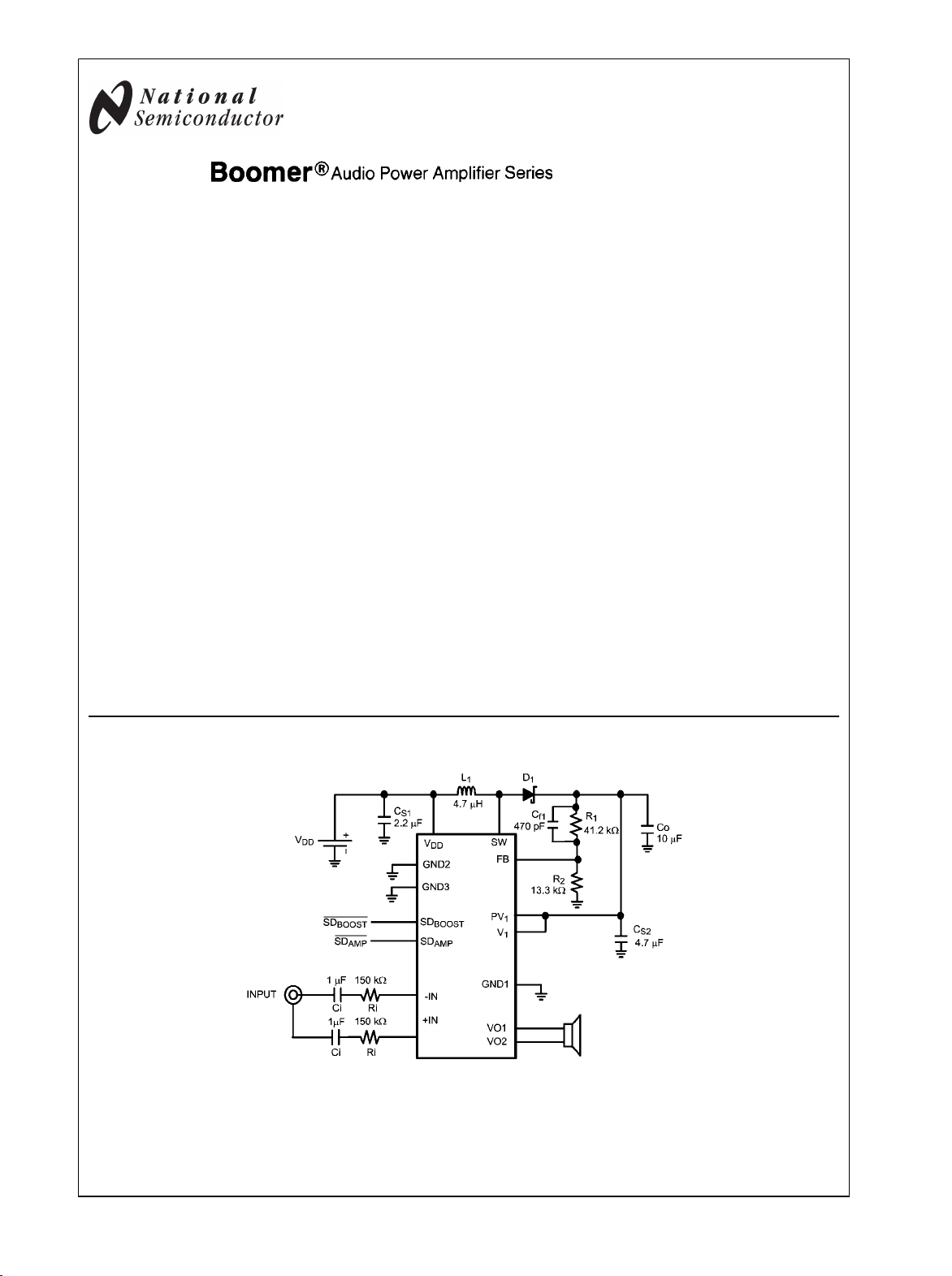
Typical Application
20123266
FIGURE 1. Typical LM48510 Audio Amplifier Application Circuit
Boomer® is a registered trademark of National Semiconductor Corporation.
© 2007 National Semiconductor Corporation 201232 www.national.com
Page 2
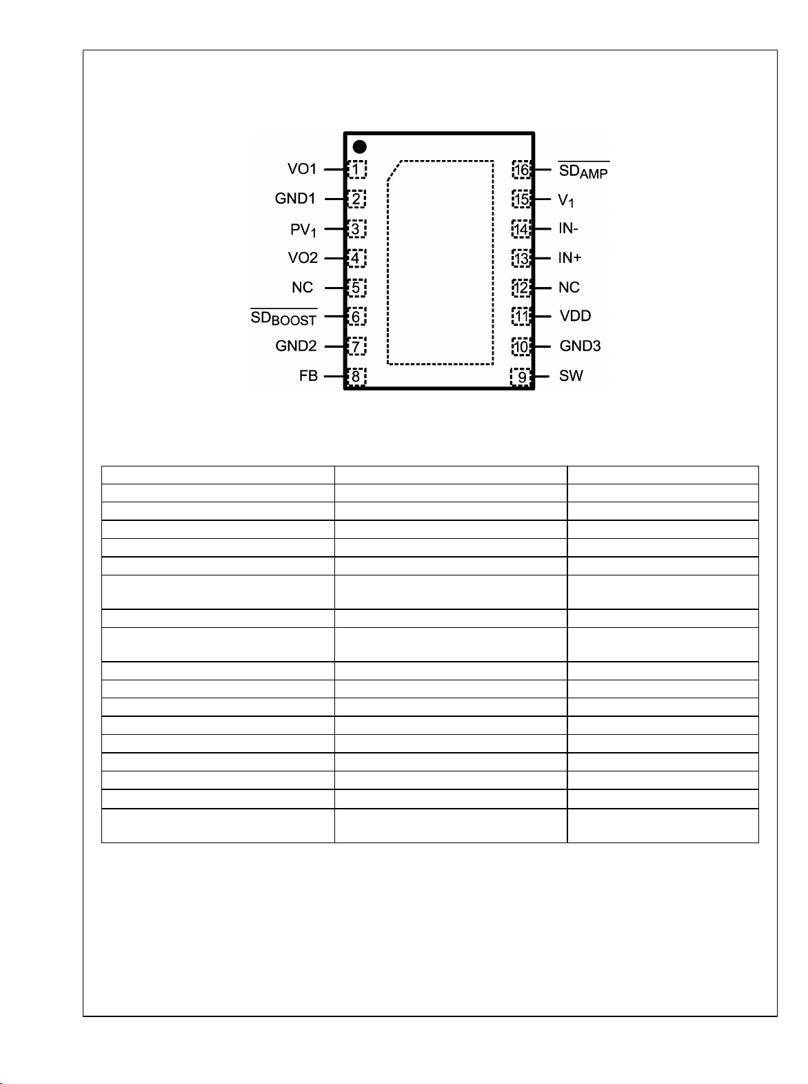
Connection Diagram
LM48510
LM48510SD
Top View
20123267
Order Number LM48510SD
See NS Package Number SDA16B
LLP-14 Pin Name Function
1 VO1 Amplifier Output
2 GND1 Ground
3 PV1 Amplifier Power Input
4 VO2 Amplifier Output
5 NC1 No Connect
6 SD
BOOST
Boost Regulator Active Low
Shutdown
7 GND2 Signal Ground (Booster)
8 FB Feedback point that connects to
external resistive divider
9 SW Drain of the Internal FET Switch
10 GND3 Power Ground (Booster)
11 VDD Power Supply
12 NC2 No Connect
13 IN+ Amplifier Non-Inverting Input
14 IN- Amplifier Inverting Input
15 V1 Amplifier Power Input
16 SD
DAP
AMP
To be soldered to board for
Amplifier Active Low Shutdown
enhanced thermal dissipation.
www.national.com 2
Page 3
LM48510
Absolute Maximum Ratings (Notes 2, 2)
If Military/Aerospace specified devices are required,
please contact the National Semiconductor Sales Office/
Thermal Resistance
θJA (SD)
37°C/W
See AN-1187 'Leadless Leadframe Packaging (LLP)'
Distributors for availability and specifications.
Supply Voltage (VDD, V1)
6V
Storage Temperature −65°C to +150°C
Input Voltage
−0.3V to VDD + 0.3V
Power Dissipation (Note 3) Internally limited
ESD Susceptibility (Note 4) 2000V
ESD Susceptibility (Note 5) 200V
Operating Ratings
Temperature Range
T
≤ TA ≤ T
MIN
MAX
Supply Voltage (VDD) 2.7V ≤ VDD ≤ 5.0V
Supply Voltage (V1) 4.5V ≤ V1 ≤ 5.5V
−40°C ≤ TA ≤ +85°C
Junction Temperature 150°C
Electrical Characteristics VDD = 3.3V (Notes 1, 2)
The following specifications apply for VDD = 3.3V, PV1 = V1 = 5.0V, AV = 6dB (Ri = 150kΩ), RL = 15µH + 8Ω +15µH, fIN = 1kHz,
unless otherwise specified. Limits apply for TA = 25°C.
Symbol Parameter Conditions LM48510 Units
I
I
V
V
T
V
P
DD
SD
SDIH
SDIL
WU
OS
O
Quiescent Power Supply Current
Shutdown Current
Shutdown Voltage Input High
Shutdown Voltage Input Low
Wake-up Time 17
Output Offset Voltage 10 mV
Output Power
THD+N Total Harmonic Distortion + Noise
VIN = 0, R
SD
AMP
LOAD
= SD
= ∞
BOOST
= GND
(Note 9)
SD1 Boost
SD2 Amplifier
SD1 Boost
SD2 Amplifier
RL = 15μH + 4Ω + 15μH
THD+N = 1% (max),
f = 1kHz, 22kHz, BW
VDD = 3.3V
RL = 15μH + 8Ω + 15μH
THD+N = 1% (max),
f = 1kHz, 22kHz, BW
VDD = 3.3V
RL = 15μH + 4Ω + 15μH
THD+N = 10% (max),
f = 1kHz, 22kHz, BW
VDD = 2.7V
VDD = 3.3V
RL = 15μH + 8Ω + 15μH
THD+N = 10% (max),
f = 1kHz, 22kHz, BW
VDD = 2.7V
VDD = 3.3V
PO = 500mW, f = 1kHz,
RL = 15μH + 8Ω + 15μH,
VDD = 2.7V
PO = 500mW, f = 1kHz,
RL = 15μH + 8Ω + 15μH,
VDD = 3.3V
Typical
(Note 6)
6.06 8.75 mA (max)
0.01 1
1.7
1.2 0.9 W (min)
1.11
1.9
0.98
1.55
0.06 %
0.07
Limit
(Notes 7, 8)
1.5
1.4
0.5
0.4
(Limits)
μA (max)
V (min)
V (min)
V (max)
V (max)
μs
W
W
W
W
W
%
3 www.national.com
Page 4
Symbol Parameter Conditions LM48510 Units
LM48510
ε
OS
Output Noise
VDD = 3.3V, f = 20Hz – 20kHz
Inputs to AC GND, No weighting
input referred
VDD = 3.3V, f = 20Hz – 20kHz
Inputs to AC GND, A weighted
Typical
(Note 6)
67
47
Limit
(Notes 7, 8)
input referred
A
V
Gain
PSRR Power Supply Rejection Ratio
CMRR Common Mode Rejection Ratio
η
V
FB
Note 1: All voltages are measured with respect to the GND pin, unless otherwise specified.
Note 2: Absolute Maximum Ratings indicate limits beyond which damage to the device may occur. Operating Ratings indicate conditions for which the device is
functional, but do not guarantee specific performance limits. Electrical Characteristics state DC and AC electrical specifications under particular test conditions
which guarantee specific performance limits. This assumes that the device is within the Operating Ratings. Specifications are not guaranteed for parameters
where no limit is given, however, the typical value is a good indication of device performance.
Note 3: The maximum power dissipation must be derated at elevated temperatures and is dictated by T
allowable power dissipation is P
Note 4: Human body model, 100pF discharged through a 1.5kΩ resistor.
Note 5: Machine Model, 220pF–240pF discharged through all pins.
Note 6: Typicals are measured at 25°C and represent the parametric norm.
Note 7: Limits are guaranteed to National's AOQL (Average Outgoing Quality Level).
Note 8: Datasheet min/max specification limits are guaranteed by design, test, or statistical analysis.
Note 9: Shutdown current is measured with components R1 and R2 removed.
Note 10: Feedback pin reference voltage is measured with the Audio Amplifier disconnected from the Boost converter (the Boost converter is unloaded).
Efficiency
Feedback Pin Reference Voltage (Note 10) 1.24
= (T
DMAX
− TA) / θJA or the given in Absolute Maximum Ratings, whichever is lower.
JMAX
V
RIPPLE
f
RIPPLE =
V
RIPPLE
f
RIPPLE =
V
RIPPLE
f
RIPPLE =
V
RIPPLE
= 200mV
= 217Hz
= 200mV
= 1kHz
= 200mV
= 10kHz
= 1V
P-P
P-P
P-P
P-P
, f
RIPPLE
Sine,
Sine,
Sine,
= 217Hz
PO = 1W, f = 1kHz,
RL = 15μH + 8Ω + 15μH, VDD = 3.3V
, θJA, and the ambient temperature, TA. The maximum
JMAX
300kΩ/R
i
89 dB
83
55
70
76
(Limits)
µV
RMS
µV
RMS
V/V
dB
dB
dB
%
V
www.national.com 4
Page 5
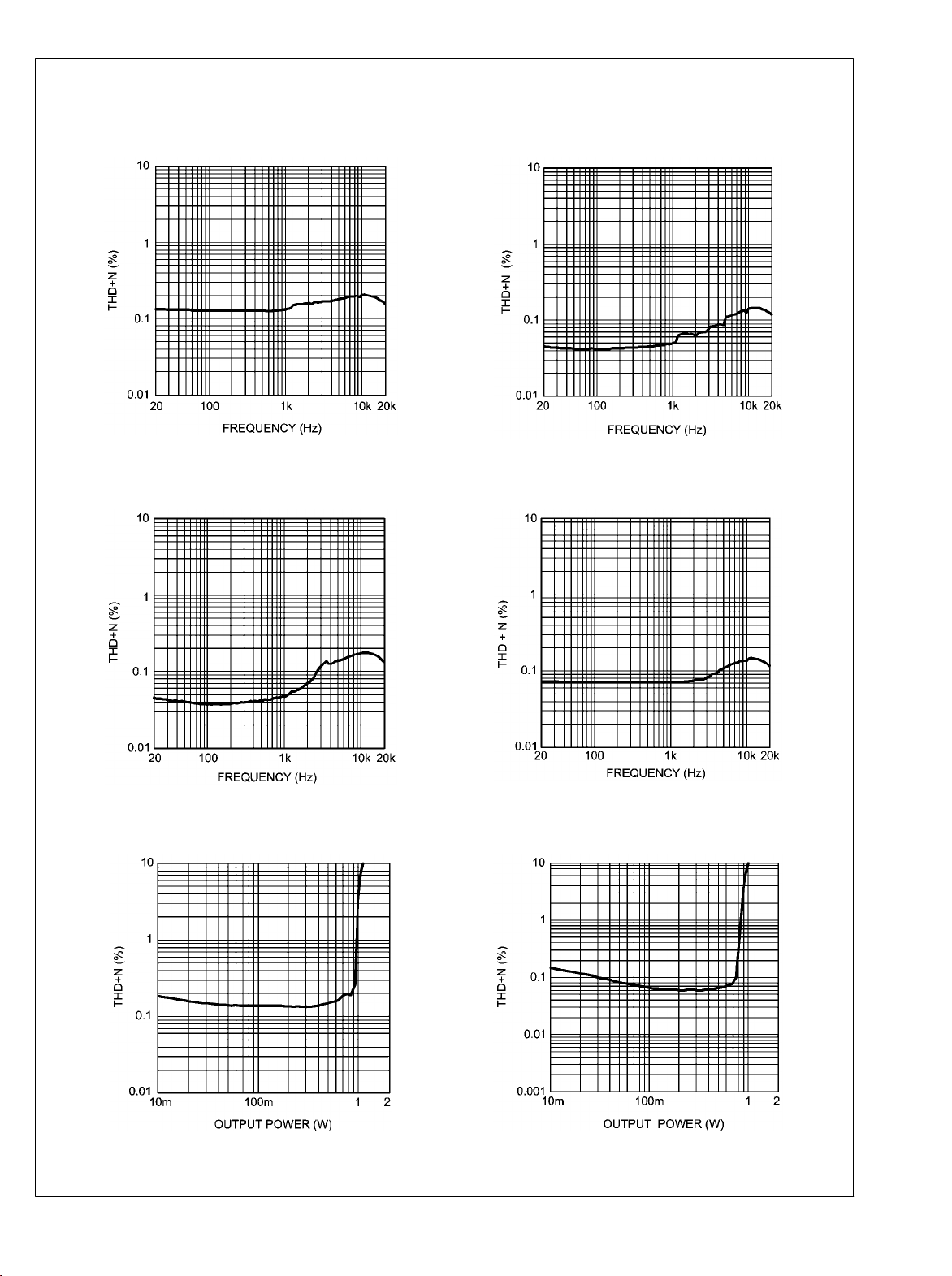
Typical Performance Characteristics
LM48510
THD+N vs Frequency
VDD = 2.7V, RL = 15μH + 4Ω + 15μH
THD+N vs Frequency
VDD = 3.3V, RL = 15μH + 4Ω + 15μH
20123237
THD+N vs Frequency
VDD = 2.7V, RL = 15μH + 8Ω + 15μH
20123250
THD+N vs Frequency
VDD = 3.3V, RL = 15μH + 8Ω + 15μH
THD+N vs Output Power
VDD = 2.7V, RL = 15μH + 4Ω + 15μH
20123239
20123241
20123240
THD+N vs Output Power
VDD = 2.7V, RL = 15μH + 8Ω + 15μH
20123251
5 www.national.com
Page 6
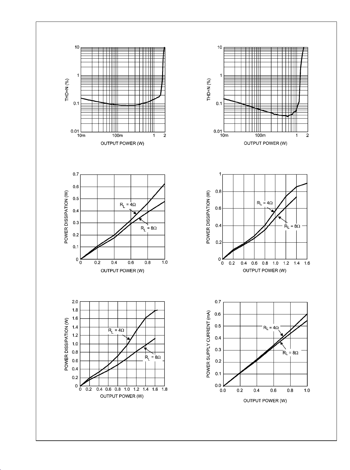
LM48510
THD+N vs Output Power
VDD = 3.3V, RL = 15μH + 4Ω + 15μH
THD+N vs Output Power
VDD = 3.3V, RL = 15μH + 8Ω + 15μH
Power Dissipation vs Output Power
VDD = 2.7V
Power Dissipation vs Output Power
VDD = 4.2V
20123243
20123234
20123244
Power Dissipation vs Output Power
VDD = 3.3V
20123235
Power Supply Current vs Output Power
VDD = 2.7V
20123236
www.national.com 6
20123229
Page 7

LM48510
Power Supply Current vs Output Power
VDD = 3.3V
20123230
PSRR vs. Frequency
VDD = 3.3V, RL = 15μH + 8Ω + 15μH
Power Supply Current vs Output Power
VDD = 4.2V
20123231
CMRR vs Frequency
VDD = 3.3V, RL = 15μH + 8Ω + 15μH
Supply Current vs. Supply Voltage
RL = no load
20123232
20123233
20123212
SW Current vs. Duty Cycle
20123245
7 www.national.com
Page 8

LM48510
Feedback Voltage vs. Temperature
Feedback Bias Current vs. Temperature
Max Duty Cycle vs. Temperature
R
vs. V
DS(ON)
IN
20123224
20123246
R
vs. Temperature
DS(ON)
Output Power vs. Efficiency
RL = 4Ω
20123225
20123227
20123228
www.national.com 8
201232c2
Page 9

LM48510
Output Power vs. Efficiency
RL = 8Ω
201232c3
Boost Converter Max. Load Current
vs. V
DD
20123265
9 www.national.com
Page 10

Application Information
GENERAL AMPLIFIER FUNCTION
LM48510
The audio amplifier portion of LM48510 is a Class D featuring
a filterless modulation scheme. The differential outputs of the
device switch at 300kHz from PV1 to GND. When there is no
input signal applied, the two outputs (VO1 and VO2) switch
with a 50% duty cycle, with both outputs in phase. Because
the outputs of the Class D are differential, the two signals
cancel each other. This results in no net voltage across the
speaker, thus there is no load current during an idle state,
conserving power.
With an input signal applied, the duty cycle (pulse width) of
the Class D outputs changes. For increasing output voltages,
the duty cycle of VO1 increases, while the duty cycle of VO2
decreases. For decreasing output voltages, the converse occurs, the duty cycle of VO2 increases while the duty cycle of
VO1 decreases. The difference between the two pulse widths
yields the differential output voltage.
OPERATING RATINGS
The LM48510 has independent power supplies for the Class
D audio power amplifier (PV1, V1) and the Boost Converter
(VDD). The Class D amplifier operating rating is 2.4V≤(PV1,
V1)≤5.5V when being used without the Boost.
Note the output voltage (PV1, V1) has to be more than VDD.
DIFFERENTIAL AMPLIFIER EXPLANATION
As logic supply voltages continue to shrink, designers are increasingly turning to differential analog signal handling to
preserve signal to noise ratios with restricted voltage swing.
The amplifier portion of the LM48510 is a fully differential amplifier that features differential input and output stages. A
differential amplifier amplifies the difference between the two
input signals. Traditional audio power amplifiers have typically offered only single-ended inputs resulting in a 6dB reduction in signal to noise ratio relative to differential inputs. The
amplifier also offers the possibility of DC input coupling which
eliminates the two external AC coupling, DC blocking capacitors. The amplifier can be used, however, as a single ended
input amplifier while still retaining it's fully differential benefits.
In fact, completely unrelated signals may be placed on the
input pins. The amplifier portion of the LM48510 simply amplifies the difference between the signals. A major benefit of
a differential amplifier is the improved common mode rejection ratio (CMRR) over single input amplifiers. The commonmode rejection characteristic of the differential amplifier
reduces sensitivity to ground offset related noise injection,
especially important in high noise applications.
AMPLIFIER DISSIPATION
In general terms, efficiency is considered to be the ratio of
useful work output divided by the total energy required to produce it with the difference being the power dissipated, typically, in the IC. The key here is “useful” work. For audio
systems, the energy delivered in the audible bands is considered useful including the distortion products of the input
signal. Sub-sonic (DC) and super-sonic components
(>22kHz) are not useful. The difference between the power
flowing from the power supply and the audio band power being transduced is dissipated in the LM48510 and in the transducer load. The amount of power dissipation in the LM48510
is very low. This is because the ON resistance of the switches
used to form the output waveforms is typically less than
0.25Ω. This leaves only the transducer load as a potential
"sink" for the small excess of input power over audio band
output power. The amplifier dissipates only a fraction of the
excess power requiring no additional PCB area or copper
plane to act as a heat sink.
BOOST CONVERTER POWER DISSIPATION
At higher duty cycles, the increased ON time of the FET
means the maximum output current will be determined by
power dissipation within the boost converter FET switch. The
switch power dissipation from ON-state conduction is calculated by Equation 1.
P
DMAX(SWITCH)
= DC x I
(AVE)2 x R
IND
DS(ON)
(1)
Where DC is the duty cycle.
There will be some switching losses as well, so some derating
needs to be applied when calculating IC power dissipation.
SHUTDOWN FUNCTION
To reduce power consumption while not in use, the amplifier
of LM48510 contains shutdown circuitry that reduces current
draw to less than 0.01µA. It is best to switch between ground
and supply (PV1, V1) for minimum current usage while in the
shutdown state. While the LM48510 may be disabled with
shutdown voltages in between ground and supply, the idle
current will be greater than the typical 0.01µA value. Increased THD may also be observed with voltages less than
VDD on the SD
pin when in PLAY mode.
AMP
The amplifier has an internal resistor connected between
GND and SD
inate any unwanted state changes when the SD
floating. The amplifier will enter the shutdown state when the
SD
pin is left floating or if not floating, when the shutdown
AMP
voltage has crossed the threshold. To minimize the supply
current while in the shutdown state, the SD
driven to GND or left floating. If the SD
GND, the amount of additional resistor current due to the in-
pins. The purpose of this resistor is to elim-
AMP
AMP
pin should be
AMP
pin is not driven to
AMP
pin is
ternal shutdown resistor can be found by Equation (2) below.
(VSD - GND) / 300kΩ (2)
With only a 0.5V difference, an additional 1.7µA of current will
be drawn while in the shutdown state.
In many applications, a microcontroller or microprocessor
output is used to control the shutdown circuitry to provide a
quick, smooth transition into shutdown. Another solution is to
use a single-pole, single-throw switch, and a pull-up resistor.
One terminal of the switch is connected to GND. The other
side is connected to the two shutdown pins and the terminal
of the pull-up resistor. The remaining resistance terminal is
connected to VDD. If the switch is open, then the external pullup resistor connected to VDD will enable the LM48510. This
scheme guarantees that the shutdown pins will not float thus
preventing unwanted state changes.
PROPER SELECTION OF EXTERNAL COMPONENTS
Proper selection of external components in applications using
integrated power amplifiers, and switching DC-DC converters, is critical for optimizing device and system performance.
Consideration to component values must be used to maximize overall system quality.
The best capacitors for use with the switching converter portion of the LM48510 are multi-layer ceramic capacitors. They
have the lowest ESR (equivalent series resistance) and high-
www.national.com 10
Page 11

LM48510
est resonance frequency, which makes them optimum for
high frequency switching converters.
When selecting a ceramic capacitor, only X5R and X7R dielectric types should be used. Other types such as Z5U and
Y5F have such severe loss of capacitance due to effects of
temperature variation and applied voltage, they may provide
as little as 20% of rated capacitance in many typical applications. Always consult capacitor manufacturer’s data curves
before selecting a capacitor. High-quality ceramic capacitors
can be obtained from Taiyo-Yuden, AVX, and Murata.
The gain of the amplifier is set by the external resistors, Ri in
Figure 1. The gain is given by Equation (3) below. Best THD
+N performance is achieved with a gain of 2V/V (6dB).
AV = 2 * 150kΩ / Ri (V/V) (3)
It is recommended that resistors with 1% tolerance or better
be used to set the gain of the amplifier. The Ri resistors should
be placed close to the input pins of the amplifier. Keeping the
input traces close to each other and of the same length in a
high noise environment will aid in noise rejection due to the
good CMRR of the Class D. Noise coupled onto input traces
which are physically close to each other will be common mode
and easily rejected by the amplifier.
Input capacitors may be needed for some applications or
when the source is single-ended (see Figure1). Input capacitors are needed to block any DC voltage at the source so that
the DC voltage seen between the input terminals of the Class
D is 0V. Input capacitors create a high-pass filter with the input
resistors, Ri. The –3dB point of the high-pass filter is found
using Equation (4) below.
fC = 1 / (2πRi Ci ) (Hz) (4)
The input capacitors may also be used to remove low audio
frequencies. Small speakers cannot reproduce low bass frequencies so filtering may be desired . When the Class D is
using a single-ended source, power supply noise on the
ground is seen as an input signal by the +IN input pin that is
capacitor coupled to ground. Setting the high-pass filter point
above the power supply noise frequencies, 217Hz in a GSM
phone, for example, will filter out this noise so it is not amplified and heard on the output. Capacitors with a tolerance of
10% or better are recommended for impedance matching.
POWER SUPPLY BYPASSING FOR AMPLIFIER
As with any amplifier, proper supply bypassing is critical for
low noise performance and high power supply rejection. The
capacitor (Cs2, see Figure 1) location on both PV1 and V1 pin
should be as close to the device as possible.
SELECTING INPUT CAPACITOR FOR AUDIO AMPLIFIER
One of the major considerations is the closedloop bandwidth
of the amplifier. To a large extent, the bandwidth is dictated
by the choice of external components shown in Figure 1. The
input coupling capacitor, Ci, forms a first order high pass filter
which limits low frequency response. This value should be
chosen based on needed frequency response for a few distinct reasons.
High value input capacitors are both expensive and space
hungry in portable designs. Clearly, a certain value capacitor
is needed to couple in low frequencies without severe attenuation. But ceramic speakers used in portable systems,
whether internal or external, have little ability to reproduce
signals below 100Hz to 150Hz. Thus, using a high value input
capacitor may not increase actual system performance.
In addition to system cost and size, click and pop performance
is affected by the value of the input coupling capacitor, Ci. A
high value input coupling capacitor requires more charge to
reach its quiescent DC voltage (nominally 1/2 VDD). This
charge comes from the output via the feedback and is apt to
create pops upon device enable. Thus, by minimizing the capacitor value based on desired low frequency response, turnon pops can be minimized.
SELECTING OUTPUT CAPACITOR (CO) FOR BOOST CONVERTER
A single 4.7µF to 10µF ceramic capacitor will provide sufficient output capacitance for most applications. If larger
amounts of capacitance are desired for improved line support
and transient response, tantalum capacitors can be used.
Aluminum electrolytics with ultra low ESR such as Sanyo Oscon can be used, but are usually prohibitively expensive.
Typical electrolytic capacitors are not suitable for switching
frequencies above 500 kHz because of significant ringing and
temperature rise due to self-heating from ripple current. An
output capacitor with excessive ESR can also reduce phase
margin and cause instability.
In general, if electrolytics are used, it is recommended that
they be paralleled with ceramic capacitors to reduce ringing,
switching losses, and output voltage ripple.
SELECTING INPUT CAPACITOR (Cs1) FOR BOOST CONVERTER
An input capacitor is required to serve as an energy reservoir
for the current which must flow into the coil each time the
switch turns ON. This capacitor must have extremely low
ESR, so ceramic is the best choice. A nominal value of 4.7µF
is recommended, but larger values can be used. Since this
capacitor reduces the amount of voltage ripple seen at the
input pin, it also reduces the amount of EMI passed back
along that line to other circuitry.
SETTING THE OUTPUT VOLTAGE (V1) OF BOOST CONVERTER
The output voltage is set using the external resistors R1 and
R2 (see Figure 1). A value of approximately 13.3kΩ is recommended for R2 to establish a divider current of approximately 92µA. R1 is calculated using the formula:
R1 = R2 X (V1/1.23 − 1) (5)
FEED-FORWARD COMPENSATION FOR BOOST CONVERTER
Although the LM48510's internal Boost converter is internally
compensated, the external feed-forward capacitor Cf1 is required for stability (see Figure 1). Adding this capacitor puts
a zero in the loop response of the converter. The recommended frequency for the zero fz should be approximately
6kHz. Cf1 can be calculated using the formula:
Cf1 = 1 / (2π X R1 X fz) (6)
SELECTING DIODES FOR BOOST
The external diode used in Figure 1 should be a Schottky
diode. A 20V diode such as the MBR0520 is recommended.
11 www.national.com
Page 12

The MBR05XX series of diodes are designed to handle a
maximum average current of 0.5A. For applications exceeding 0.5A average but less than 1A, a Microsemi UPS5817 can
LM48510
be used.
DUTY CYCLE
The maximum duty cycle of the boost converter determines
the maximum boost ratio of output-to-input voltage that the
converter can attain in continuous mode of operation. The
duty cycle for a given boost application is defined as:
Duty Cycle = V1 + V
- VDD / V1 + V
DIODE
DIODE
This applies for continuous mode operation.
INDUCTANCE VALUE
The inductor is the largest sized component and usually the
most costly. “How small can the inductor be?” The answer is
not simple and involves trade-offs in performance. Larger inductors mean less inductor ripple current, which typically
means less output voltage ripple (for a given size of output
capacitor). Larger inductors also mean more load power can
be delivered because the energy stored during each switching cycle is:
E = L/2 X (lp)2
Where lp is the peak inductor current. An important point to
observe is that the LM48510 will limit its switch current based
on peak current. This means that since lp(max) is fixed, increasing L will increase the maximum amount of power available to the load. Conversely, using too little inductance may
limit the amount of load current which can be drawn from the
output.
Best performance is usually obtained when the converter is
operated in “continuous” mode at the load current range of
interest, typically giving better load regulation and less output
ripple. Continuous operation is defined as not allowing the inductor current to drop to zero during the cycle. It should be
noted that all boost converters shift over to discontinuous operation as the output load is reduced far enough, but a larger
inductor stays “continuous” over a wider load current range.
To better understand these trade-offs, a typical application
circuit (5V to 12V boost with a 10µH inductor) will be analyzed.
We will assume:
VIN = 5V, V
= 12V, V
OUT
= 0.5V, VSW = 0.5V
DIODE
Since the frequency is 0.6MHz (nominal), the period is approximately 1.66µs. The duty cycle will be 62.5%, which
means the ON-time of the switch is 1.04µs. It should be noted
that when the switch is ON, the voltage across the inductor is
approximately 4.5V. Using the equation:
V = L (di/dt)
We can then calculate the di/dt rate of the inductor which is
found to be 0.17 A/µs during the ON-time. Using these facts,
we can then show what the inductor current will look like during operation:
- V
SW
20123248
FIGURE 2. 10μH Inductor Current
5V - 12V Boost (LM48510)
During the 1.04µs ON-time, the inductor current ramps up
0.176A and ramps down an equal amount during the OFFtime. This is defined as the inductor “ripple current”. A similar
analysis can be performed on any boost converter, to make
sure the ripple current is reasonable and continuous operation will be maintained at the typical load current values.
MAXIMUM SWITCH CURRENT
The maximum FET switch current available before the current
limiter cuts in is dependent on duty cycle of the application.
This is illustrated in a graph in the typical performance characterization section which shows typical values of switch
current as a function of effective (actual) duty cycle.
CALCULATING OUTPUT CURRENT OF BOOST
CONVERTER (I
AMP
)
As shown in Figure 2 which depicts inductor current, the load
current is related to the average inductor current by the relation:
I
= I
LOAD
(AVG) x (1 - DC) (7)
IND
Where "DC" is the duty cycle of the application. The switch
current can be found by:
ISW = I
(AVG) + 1/2 (I
IND
) (8)
RIPPLE
Inductor ripple current is dependent on inductance, duty cycle, input voltage and frequency:
I
= DC x (VIN-VSW) / (f x L) (9)
RIPPLE
combining all terms, we can develop an expression which allows the maximum available load current to be calculated:
I
(max) = (1–DC)x(ISW(max)–DC(VIN-VSW))/2fL (10)
LOAD
The equation shown to calculate maximum load current takes
into account the losses in the inductor or turn-OFF switching
losses of the FET and diode.
DESIGN PARAMETERS VSW AND I
SW
The value of the FET ON voltage (referred to as VSW in equations 4 thru 7) is dependent on load current. A good approximation can be obtained by multiplying the R
times the average inductor current.
DS(ON)
of the FET
www.national.com 12
Page 13

LM48510
FET on resistance increases at VIN values below 5V, since
the internal N-FET has less gate voltage in this input voltage
range (see Typical Performance Characteristics curves).
Above VIN = 5V, the FET gate voltage is internally clamped to
5V.
The maximum peak switch current the device can deliver is
dependent on duty cycle. For higher duty cycles, see Typical
Performance Characteristics curves.
INDUCTOR SUPPLIERS
Recommended suppliers of inductors for the LM48510 include, but are not limited to Taiyo-Yuden, Sumida, Coilcraft,
Panasonic, TDK and Murata. When selecting an inductor,
make certain that the continuous current rating is high enough
to avoid saturation at peak currents. A suitable core type must
be used to minimize core (switching) losses, and wire power
losses must be considered when selecting the current rating.
PCB LAYOUT GUIDELINES
High frequency boost converters require very careful layout
of components in order to get stable operation and low noise.
All components must be as close as possible to the LM48510
device. It is recommended that a four layer PCB be used so
that internal ground planes are available.
Some additional guidelines to be observed:
1. Keep the path between L1, D1, and Co extremely short.
Parasitic trace inductance in series with D1 and Co will increase noise and ringing.
2. The feedback components R1, R2 and Cf1 must be kept
close to the FB pin to prevent noise injection on the FB pin
trace.
3. If internal ground planes are available (recommended) use
vias to connect directly to ground at pin 2 of U1, as well as the
negative sides of capacitors Cs1 and Co.
GENERAL MIXED-SIGNAL LAYOUT RECOMMENDATION
This section provides practical guidelines for mixed signal
PCB layout that involves various digital/analog power and
ground traces. Designers should note that these are only
"rule-of-thumb" recommendations and the actual results will
depend heavily on the final layout.
Power and Ground Circuits
For two layer mixed signal design, it is important to isolate the
digital power and ground trace paths from the analog power
and ground trace paths. Star trace routing techniques (bringing individual traces back to a central point rather than daisy
chaining traces together in a serial manner) can have a major
impact on low level signal performance. Star trace routing
refers to using individual traces to feed power and ground to
each circuit or even device. This technique will take require a
greater amount of design time but will not increase the final
price of the board. The only extra parts required may be some
jumpers.
Single-Point Power / Ground Connection
The analog power traces should be connected to the digital
traces through a single point (link). A "Pi-filter" can be helpful
in minimizing high frequency noise coupling between the analog and digital sections. It is further recommended to place
digital and analog power traces over the corresponding digital
and analog ground traces to minimize noise coupling.
Placement of Digital and Analog Components
All digital components and high-speed digital signals traces
should be located as far away as possible from analog components and circuit traces.
Avoiding Typical Design / Layout Problems
Avoid ground loops or running digital and analog traces parallel to each other (side-by-side) on the same PCB layer.
When traces must cross over each other do it at 90 degrees.
Running digital and analog traces at 90 degrees to each other
from the top to the bottom side as much as possible will minimize capacitive noise coupling and crosstalk.
13 www.national.com
Page 14

LM48510
20123268
FIGURE 3. Demo Board Schematic Reference
www.national.com 14
Page 15

Demonstration Board Layout
LM48510
FIGURE 4. Top Layer Silkscreen
FIGURE 6. GND Layer (middle 1)
20123298
20123262
FIGURE 5. Top Trace Layer
FIGURE 7. Power Trace Layer (middle 2)
20123264
20123263
FIGURE 8. Bottom Layer
20123261
FIGURE 9. Bottom Silkscreen
15 www.national.com
20123260
Page 16

Build Of Material
Designator Description Footprint Quantity Value
LM48510
Cf1 CHIP CAPACITOR GENERIC CAP 0805 1 470pF
CINA CHIP CAPACITOR GENERIC CAP 1210 1
CINB CHIP CAPACITOR GENERIC CAP 1210 1
Co CHIP CAPACITOR GENERIC CAP 1210 1
Cs1 CHIP CAPACITOR GENERIC CAP 1210 1
Cs2 CHIP CAPACITOR GENERIC CAP 1210 1
D1 SCHOTTKY DIO DIODE MBR0520 IR 1
L1 IND_COILCRAFT-DO1813P 1
R1 CHIP RESISTOR GENERIC RES 0805 1 41.2K
R2 CHIP RESISTOR GENERIC RES 0805 1 13.3K
RINA CHIP RESISTOR GENERIC RES 0805 1 150K
RINB CHIP RESISTOR GENERIC RES 0805 1 150K
1μF
1μF
10μF
2.2μF
4.7μF
4.7μH
www.national.com 16
Page 17

Revision History
Rev Date Description
1.0 11/16/06 Initial release.
1.1 03/07/07 Changed the Limit value on the V
SDIH
and V
to 1.5 and 0.5 respectively.
SDIL
LM48510
17 www.national.com
Page 18

Physical Dimensions inches (millimeters) unless otherwise noted
LM48510
LLP Package
Order Number LM48510SD
NS Package Number SDA16B
www.national.com 18
Page 19

Notes
LM48510
19 www.national.com
Page 20

Notes
THE CONTENTS OF THIS DOCUMENT ARE PROVIDED IN CONNECTION WITH NATIONAL SEMICONDUCTOR CORPORATION
(“NATIONAL”) PRODUCTS. NATIONAL MAKES NO REPRESENTATIONS OR WARRANTIES WITH RESPECT TO THE ACCURACY
OR COMPLETENESS OF THE CONTENTS OF THIS PUBLICATION AND RESERVES THE RIGHT TO MAKE CHANGES TO
SPECIFICATIONS AND PRODUCT DESCRIPTIONS AT ANY TIME WITHOUT NOTICE. NO LICENSE, WHETHER EXPRESS,
LM48510 Boosted Class D Audio Power Amplifier
IMPLIED, ARISING BY ESTOPPEL OR OTHERWISE, TO ANY INTELLECTUAL PROPERTY RIGHTS IS GRANTED BY THIS
DOCUMENT.
TESTING AND OTHER QUALITY CONTROLS ARE USED TO THE EXTENT NATIONAL DEEMS NECESSARY TO SUPPORT
NATIONAL’S PRODUCT WARRANTY. EXCEPT WHERE MANDATED BY GOVERNMENT REQUIREMENTS, TESTING OF ALL
PARAMETERS OF EACH PRODUCT IS NOT NECESSARILY PERFORMED. NATIONAL ASSUMES NO LIABILITY FOR
APPLICATIONS ASSISTANCE OR BUYER PRODUCT DESIGN. BUYERS ARE RESPONSIBLE FOR THEIR PRODUCTS AND
APPLICATIONS USING NATIONAL COMPONENTS. PRIOR TO USING OR DISTRIBUTING ANY PRODUCTS THAT INCLUDE
NATIONAL COMPONENTS, BUYERS SHOULD PROVIDE ADEQUATE DESIGN, TESTING AND OPERATING SAFEGUARDS.
EXCEPT AS PROVIDED IN NATIONAL’S TERMS AND CONDITIONS OF SALE FOR SUCH PRODUCTS, NATIONAL ASSUMES NO
LIABILITY WHATSOEVER, AND NATIONAL DISCLAIMS ANY EXPRESS OR IMPLIED WARRANTY RELATING TO THE SALE
AND/OR USE OF NATIONAL PRODUCTS INCLUDING LIABILITY OR WARRANTIES RELATING TO FITNESS FOR A PARTICULAR
PURPOSE, MERCHANTABILITY, OR INFRINGEMENT OF ANY PATENT, COPYRIGHT OR OTHER INTELLECTUAL PROPERTY
RIGHT.
LIFE SUPPORT POLICY
NATIONAL’S PRODUCTS ARE NOT AUTHORIZED FOR USE AS CRITICAL COMPONENTS IN LIFE SUPPORT DEVICES OR
SYSTEMS WITHOUT THE EXPRESS PRIOR WRITTEN APPROVAL OF THE CHIEF EXECUTIVE OFFICER AND GENERAL
COUNSEL OF NATIONAL SEMICONDUCTOR CORPORATION. As used herein:
Life support devices or systems are devices which (a) are intended for surgical implant into the body, or (b) support or sustain life and
whose failure to perform when properly used in accordance with instructions for use provided in the labeling can be reasonably expected
to result in a significant injury to the user. A critical component is any component in a life support device or system whose failure to perform
can be reasonably expected to cause the failure of the life support device or system or to affect its safety or effectiveness.
National Semiconductor and the National Semiconductor logo are registered trademarks of National Semiconductor Corporation. All other
brand or product names may be trademarks or registered trademarks of their respective holders.
Copyright© 2007 National Semiconductor Corporation
For the most current product information visit us at www.national.com
www.national.com
National Semiconductor
Americas Customer
Support Center
Email:
new.feedback@nsc.com
Tel: 1-800-272-9959
National Semiconductor Europe
Customer Support Center
Fax: +49 (0) 180-530-85-86
Email: europe.support@nsc.com
Deutsch Tel: +49 (0) 69 9508 6208
English Tel: +49 (0) 870 24 0 2171
Français Tel: +33 (0) 1 41 91 8790
National Semiconductor Asia
Pacific Customer Support Center
Email: ap.support@nsc.com
National Semiconductor Japan
Customer Support Center
Fax: 81-3-5639-7507
Email: jpn.feedback@nsc.com
Tel: 81-3-5639-7560
 Loading...