

Page 1
LM4850
Mono 1.5 W / Stereo 300 mW Power Amplifier
General Description
The LM4850 is an audio power amplifier capable of delivering 1.5W (typ) of continuous average power into a mono 4Ω
bridged-tied load (BTL) with 1% THD+N or 95mW per channel of continuous average power into stereo 32Ω
single-ended (SE) loads with 1% THD+N, using a 5V power
supply.
The LM4850 can automatically switch between mono BTL
and stereo SE modes utilizing a headphone sense pin. It is
ideal for any system that provides both a monaural speaker
output and a stereo line or headphone output
Boomer audio power amplifiers were designed specifically to
provide high quality output power with a minimal amount of
external components. Since the LM4850 does not require
bootstrap capacitors or snubber networks, it is optimally
suited for low-power portable systems.
The LM4850 features an externally controlled, micropower
consumption shutdown mode and thermal shutdown protection. The unity-gain stable LM4850’s gain is set by external
gain-setting resistors
Note 1: An LM4850LD that has been properly mounted to a circuit board will
deliver 1.9W into 3Ω (at 1% THD+N). The other package options for the
LM4850 will deliver 1.1W into 8Ω (at 1% THD+N). See Application Infor-
mation sections for further information concerning the LM4850LD,
LM4850MM, and LM4850MT.
Key Specifications
n Output Power at 1% THD+N, 1kHz:
n LM4850LD 3Ω BTL 1.9W (typ)
n LM4850LD 4Ω BTL 1.7W (typ)
n LM4850MM, MT 4Ω BTL 1.5W (typ)
n LM4850LD, MM, MT 8Ω BTL 1.1W (typ)
n LM4850LD, MM, MT 8Ω SE 300mW (typ)
n LM4850LD, MM, MT 32Ω SE 95mW (typ)
n THD+N at 1kHz, 95mW into 32Ω SE 1% (typ)
n Single Supply Operation 2.4 to 5.5V
n Shutdown Current 44µA (typ)
Features
n Mono 1.5W BTL or stereo 300mW output
n Headphone sense
n “Click and pop” suppression circuitry
n No bootstrap capacitors required
n Thermal shutdown protection
n Unity-gain stable
n LLP, TSSOP, and MSOP packaging
Applications
n Portable computers
n Desktop computers
n PDA’s
n Handheld games
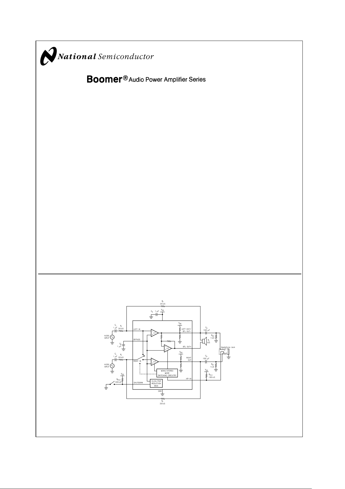
Typical Application
Boomer®is a registered trademark of National Semiconductor Corporation.
20001031
FIGURE 1. Typical Audio Amplifier Application Circuit
July 2002
LM4850 Mono 1.5 W / Stereo 300 mW Power Amplifier
© 2002 National Semiconductor Corporation DS200010 www.national.com
Page 2
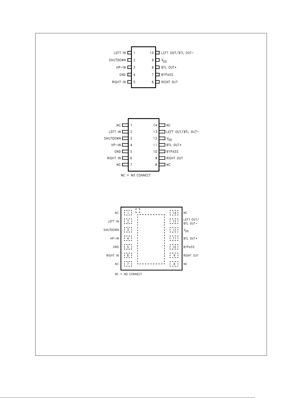
Connection Diagrams
20001051
Top View
10 Lead MSOP
Order Number LM4850MM
See NS Package Number MUB10A
20001052
Top View
14 Lead TSSOP
Order Number LM4850MT
See NS Package Number MTC14
20001002
Top View
14 Lead LLP
Order Number LM4850LD
See NS Package Number LDA14A
LM4850
www.national.com 2
Page 3
Absolute Maximum Ratings (Note 3)
If Military/Aerospace specified devices are required,
please contact the National Semiconductor Sales Office/
Distributors for availability and specifications.
Supply Voltage 6.0V
Storage Temperature −65˚C to +150˚C
ESD Susceptibility (Note 5) 3.5kV
ESD Machine model (Note 8) 250V
Junction Temperature (T
J
) 150˚C
Solder Information (Note 2)
Small Outline Package
Vapor Phase (60 sec.) 215˚C
Infrared (15 sec.) 220˚C
Thermal Resistance
θ
JA
(typ) —MUB10A 194˚C/W
θ
JC
(typ) — MUB10A 52˚C/W
θ
JA
(typ) — MTC14 150˚C/W
θ
JC
(typ) — MTC14 40˚C/W
θ
JA
(typ) — LDA14A (Note 10) 56˚C/W
θ
JC
(typ) — LDA14A 4.3˚C/W
Operating Ratings (Note 3)
Temperature Range
−40˚C ≤ to 85˚C
Supply Voltage V
DD
2.4V ≤ VDD≤ 5.5V
Note 2: See AN-450 ’Surface Mounting and their effects on Product Reliability’ for other methods of soldering surface mount devices.
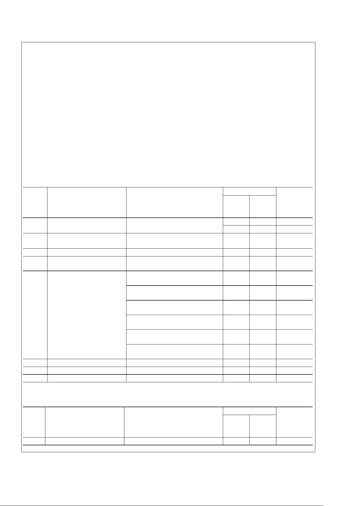
Electrical Characteristics (Notes 3, 9)
The following specifications apply for VDD= 5.0V, TA= 25˚C unless otherwise specified.
Symbol Parameter Conditions LM4850 Units
(Limits)
Typical
(Note 6)
Limit
(Note 7)
V
DD
Supply Voltage 2.4 V (min)
5.5 V (max)
I
DD
Supply Current BTL Mode; VIN= 0V; IO= 0A 2.4 7.0 mA
SE Mode; V
IN
= 0V; IO= 0A 2.4 7.0 mA
I
SD
Shutdown Current SD Mode 44 µA
V
OS
Output Offset Voltage BTL Mode; AV=2
BTL OUT+ to BTL OUT−
5.0 40 mV
P
O
Output Power LM4850LD; BTL Mode; RL=3Ω
THD+N = 1% (Note 11)
1.9 W
LM4850LD; BTL Mode; RL=4Ω
THD+N = 1% (Note 11)
1.7 W
LM4850MT, MM; BTL Mode; R
L
=4Ω
THD+N = 1%
1.5 W
BTL Mode; R
L
=8Ω
THD+N = 1%
1.1 W
SE Mode; RL=8Ω
THD+N = 1%
300 mW
SE Mode; R
L
=32Ω
THD+N = 1%
95 mW
V
IH
Shutdown Input Voltage High Is<80µA 2.0 V (min)
V
IL
Shutdown Input Voltage Low Is>0.5mA 0.8 V (max)
Crosstalk Channel Seperation SE Mode, R
L
=32Ω; f = 1kHz 73 dB
Electrical Characteristics (Notes 3, 9)
The following specifications apply for VDD= 3.3V, TA= 25˚C unless otherwise specified.
Symbol Parameter Conditions LM4850 Units
(Limits)
Typical
(Note 6)
Limit
(Note 7)
I
DD
Supply Current BTL Mode; VIN= 0V; IO= 0A 2.0 mA
LM4850
www.national.com3
Page 4
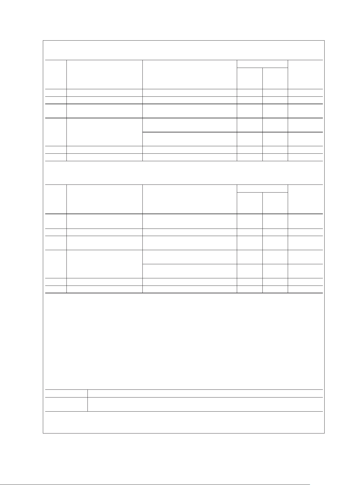
Electrical Characteristics (Notes 3, 9) (Continued)
The following specifications apply for VDD= 3.3V, TA= 25˚C unless otherwise specified.
Symbol Parameter Conditions LM4850 Units
(Limits)
Typical
(Note 6)
Limit
(Note 7)
SE Mode; V
IN
= 0V; IO= 0A 2.0 mA
I
SD
Shutdown Current SD Mode 30 µA
V
OS
Output Offset Voltage BTL Mode; AV=2
BTL OUT+ to BTL OUT−
5.0 40 mV
P
O
Output Power BTL Mode; RL=8Ω
THD+N = 1%
440 mW
SE Mode; R
L
=32Ω
THD+N = 1%
40 mW
V
IH
Shutdown Input Voltage High Is<80µA 2.0 V (min)
V
IL
Shutdown Input Voltage Low Is>0.5mA 0.8 V (max)
Electrical Characteristics(Notes 3, 9)
The following specifications apply for VDD= 2.7V, TA= 25˚C unless otherwise specified.
Symbol Parameter Conditions LM4850 Units
(Limits)
Typical
(Note 6)
Limit
(Note 7)
I
DD
Supply Current BTL Mode; VIN= 0V; IO= 0A 1.8 mA
SE Mode; V
IN
= 0V; IO= 0A 1.8 mA
I
SD
Shutdown Current SD Mode 25 µA
V
OS
Output Offset Voltage BTL Mode; AV=2
BTL OUT+ to BTL OUT−
5.0 40 mV
P
O
Output Power BTL Mode; RL=8Ω
THD+N = 1%
300 mW
SE Mode; R
L
=32Ω
THD+N = 1%
25 mW
V
IH
Shutdown Input Voltage High Is<80 µA 2.0 V (min)
V
IL
Shutdown Input Voltage Low Is>0.5mA 0.8 V (max)
Note 3: Absolute Maximum Rating indicate limits beyond which damage to the device may occur.
Note 4: Operating Ratings indicate conditions for which the device is functional, but do not guarantee specific performance limits. For guaranteed specifications and
test conditions, see the Electrical Characteristics. The guaranteed specifications apply only for the test conditions listed. Some performance characteristics may
degrade when the device is not operated under the listed test conditions.
Note 5: Human body model, 100pF discharged through a 1.5kΩ resistor.
Note 6: Typical specifications are specified at +25˚C and represent the most likely parametric norm.
Note 7: Datasheet min/max specification limits are guaranteed by design, test, or statistical analysis.
Note 8: Machine Model ESD test is covered by specification EIAJ IC-121-1981. A 200pF cap is charged to the specified voltage, then discharged directly into the
IC with no external series resistor (resistance of discharge path must be under 50Ω).
Note 9: All voltages are measured with respect to the ground pin, unless otherwise specified.
Note 10: The given θ
JA
is for a LM4850LD with the Exposed-DAP soldered to an exposed 1in2area of 1oz printed circuit board copper.
Note 11: When driving 3Ω or 4Ω loads from a 5V supply, the LM4850 must be mounted to a circuit board.
Note 12: Limits are guaranteed to National’s AOQL ( Average Outgoing Quality Level ).
External Components Description
(Refer to Figure 1.)
Components Functional Description
1. R
i
Inverting input resistance which sets the closed-loop gain in conjunction with Rf. This resistor also forms a
high pass filter with C
i
at fc= 1/(2πRiCi).
LM4850
www.national.com 4
Page 5
External Components Description (Continued)
(Refer to Figure 1.)
Components Functional Description
2. C
i
Input coupling capacitor which blocks the DC voltage at the amplifier’s input terminals. Also creates a
highpass filter with R
i
at fc= 1/(2πRiCi). Refer to the section, Proper Selection of External Components,
for an explanation of how to determine the value of C
i
.
3. R
f
Feedback resistance which sets the closed-loop gain in conjunction with Ri.
4. C
s
Supply bypass capacitor which provides power supply filtering. Refer to the Power Supply Bypassing
section for information concerning proper placement and selection of the supply bypass capacitor.
5. C
B
Bypass pin capacitor which provides half-supply filtering. Refer to the section, Proper Selection of
External Components, for information concerning proper placement and selection of C
B
.
6. C
O
Output coupling capacitor which blocks the DC voltage at the amplifier’s output. Forms a high pass filter
with the single-ended load R
L
at fO= 1/(2π RLCO).
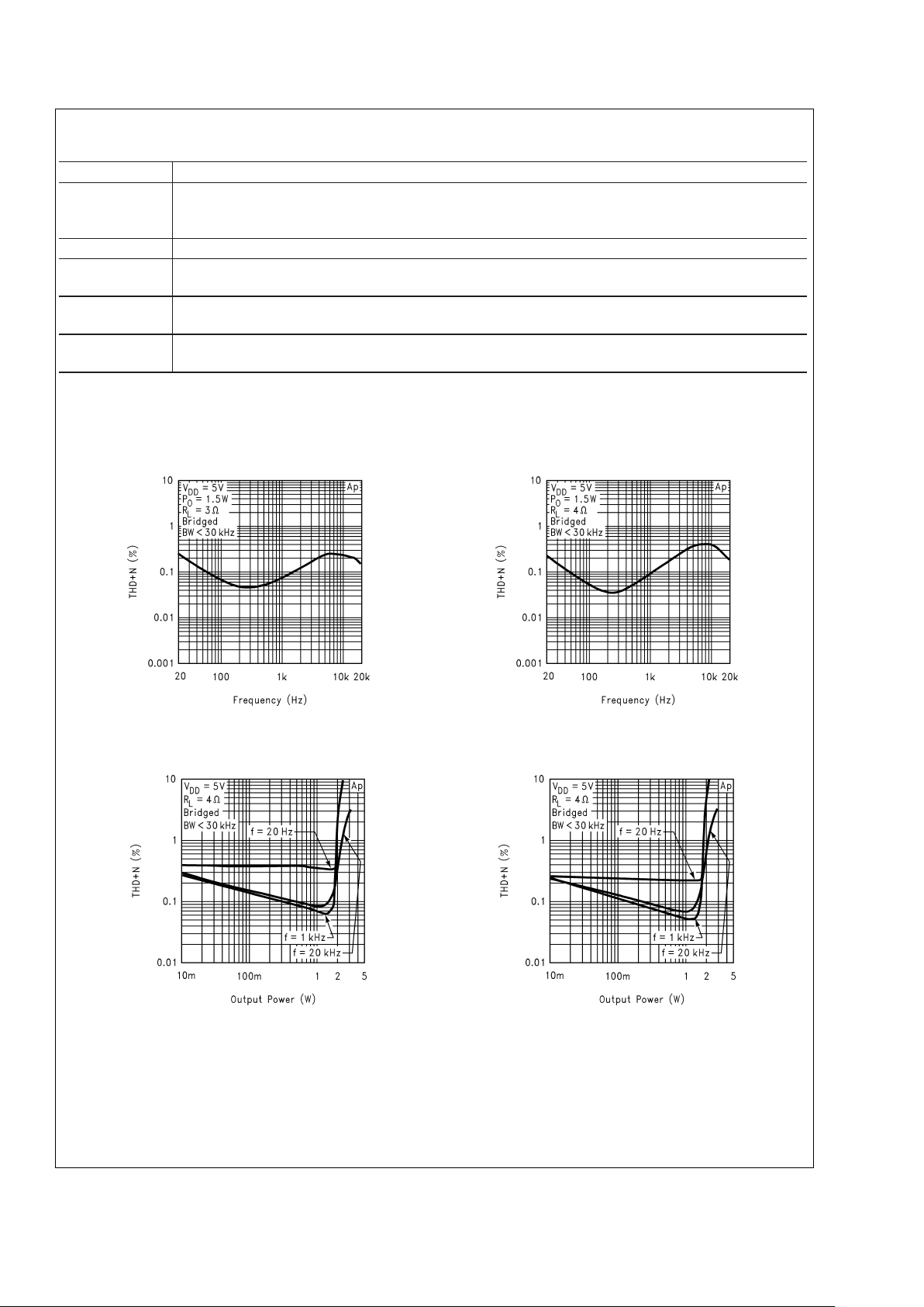
Typical Performance Characteristics
LD Specific Characteristics
LM4850LD
THD+N vs Frequency
LM4850LD
THD+N vs Frequency
20001075 20001076
LM4850LD
THD+N vs Output Power
LM4850LD
THD+N vs Output Power
20001077 20001078
LM4850
www.national.com5
Page 6
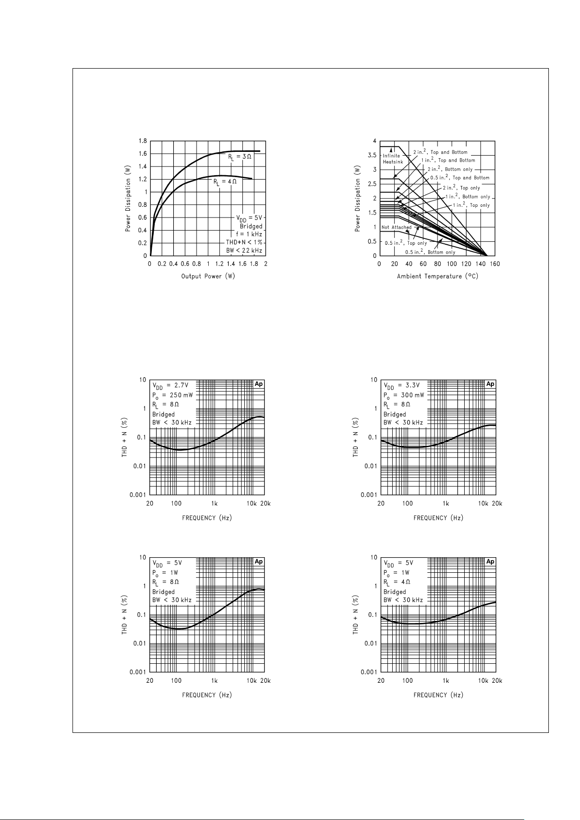
Typical Performance Characteristics
LD Specific Characteristics
(Continued)
LM4850LD
Power Dissipation vs Output Power
LM4850LD (Note 13)
Power Derating Curve
20001079
20001094
Note 13: This curve shows the LM4850LD’s thermal dissipation ability at different ambient temperatures given the exposed-DAP of the part is soldered to a plane
of 1oz. Cu with an area given in the label of each curve. This label also designated whether the plane exists on the same (top) layer as the chip, on the bottom layer,
or on both layers. Infinite heatsink and unattached (no heatsink) conditions are also shown.
Typical Performance Characteristics
Non-LD Specific Characteristics
THD+N vs Frequency THD+N vs Frequency
20001063 20001064
THD+N vs Frequency THD+N vs Frequency
20001065 20001066
LM4850
www.national.com 6
Page 7

Typical Performance Characteristics
Non-LD Specific Characteristics
(Continued)
THD+N vs Frequency THD+N vs Frequency
20001067 20001068
THD+N vs Frequency THD+N vs Output Power
20001039 20001040
THD+N vs Output Power THD+N vs Output Power
20001041 20001042
LM4850
www.national.com7
Page 8

Typical Performance Characteristics
Non-LD Specific Characteristics
(Continued)
THD+N vs Output Power THD+N vs Output Power
20001043
20001044
THD+N vs Output Power THD+N vs Output Power
20001045 20001046
THD+N vs Output Power Output Power vs Load Resistance
20001047
20001048
LM4850
www.national.com 8
Page 9

Typical Performance Characteristics
Non-LD Specific Characteristics
(Continued)
Output Power vs Load Resistance Output Power vs Supply Voltage
20001049
20001069
Output Power vs Supply Voltage Dropout Voltage vs Supply Voltage
20001071 20001072
Power Dissipation vs Output Power Power Dissipation vs Output Power
20001055 20001056
LM4850
www.national.com9
Page 10

Typical Performance Characteristics
Non-LD Specific Characteristics
(Continued)
Power Derating Curve Channel Separation
20001057
20001080
Noise Floor Open Loop Frequency Response
20001059 20001062
Supply Current vs Supply Voltage Power Supply Rejection Ratio
20001061
20001060
LM4850
www.national.com 10
Page 11

Typical Performance Characteristics
Non-LD Specific Characteristics
(Continued)
Power Supply Rejection Ratio
20001074
Application Information
BRIDGED AND SINGLE-ENDED OPERATION
As shown in Figure 1, the LM4850 contains three operational
amplifiers (A1-A3). These amplifiers can be configured for
SE or BTL modes.
In the SE mode, the LM4850 operates as a high current
output dual op amp. A1 and A3 are independent amplifiers
with an externally configured gain of A
V
=-RF/RI. The
outputs of A1 and A3 are used to drive an external set of
headphones plugged into the headphone jack. Amplifier A2
is shut down to a high output impedance state in SE mode.
This prevents any current flow into the mono bridge-tied
load, thereby muting it.
In BTL mode, A3 is shut down to a high impedance state.
The audio signal from the RIGHT IN pin is directed to the
inverting input of A1. As a result, the LEFT IN and RIGHT IN
audio signals, V
INL
and V
INR
, are summed together at the
input of A1. A2 is then activated with a closed-loop gain of A
V
= -1 fixed by two internal 20kΩ resistors. The outputs of A1
and A2 are then used to drive the mono bridged-tied load.
EXPOSED-DAP PACKAGE PCB MOUNTING
CONSIDERATION
The LM4850’s exposed-DAP (die attach paddle) package
(LD) provides a low thermal resistance between the die and
the PCB to which the part is mounted and soldered. This
allows rapid heat transfer from the die to the surrounding
PCB copper traces, ground plane, and surrounding air. The
result is a low voltage audio power amplifier that produces
1.7W at ≤ 1% THD+N with a 4Ω load. This high power is
achieved through careful consideration of necessary thermal
design. Failing to optimize thermal design may compromise
the LM4850’s high power performance and activate unwanted, though necessary, thermal shutdown protection.
The LD package must have its DAP soldered to a copper
pad on the PCB. The DAP’s PCB copper pad is connected to
a large plane of continuous unbroken copper. This plane
forms a thermal mass, heat sink, and radiation area. Place
the heat sink area on either outside plane in the case of a
two-sided PCB, or on an inner layer of a board with more
than two layers. Connect the DAP copper pad to the inner
layer or backside copper heat sink area with 4(2x2) vias. The
via diameter should be 0.012in-0.013in with a 1.27mm pitch.
Ensure efficient thermal conductivity by plating through the
vias.
Best thermal performance is achieved with the largest practical heat sink area. If the heatsink and amplifier share the
same PCB layer, a nominal 2.5in
2
area is necessary for 5V
operation with a 4Ω load. Heatsink areas not placed on the
same PCB layer as the LM4850 should be 5in
2
(min) for the
same supply voltage and load resistance. The last two area
recommendations apply for 25˚C ambient temperature. Increase the area to compensate for ambient temperatures
above 25˚C. The LM4850’s power de-rating curve in the
Typical Performance Characteristics shows the maximum
power dissipation versus temperature. An example PCB layout for the LD package is shown in the Demonstration
Board Layout section. Further detailed and specific information concerning PCB layout, fabrication, and mounting an
LD (LLP) package is available from National Semiconductor’s Package Engineering Group under application note
AN1187.
BRIDGE CONFIGURATION EXPLANATION
When the LM4850 is in BTL mode, the output of amplifier A1
serves as the input to amplifier A2, which results in both
amplifiers producing signals identical in magnitude, but out
of phase by 180˚. Consequently, the differential gain for the
mono channel is:
A
VD=VOUT
/(V
INL+VINR
)=2x(RF/RI) (1)
Driving a load differentially through the BTL OUT- and BTL
OUT+ outputs is an amplifier configuration commonly referred to as ’bridged mode’. Bridged mode operation is different from the classical single-ended amplifier configuration
where one side of its load is connected to ground.
A bridge amplifier design has a few distinct advantages over
the single-ended configuration. It drives a load differentially,
which doubles output swing for a specified supply voltage.
This produces four times the output power as that produced
by a single-ended amplifier under the same conditions. This
increase in attainable output power assumes that the amplifier is not current limited or clipped. In order to choose an
LM4850
www.national.com11
Page 12

Application Information (Continued)
amplifier’s closed-loop gain without causing excessive output signal clipping, please refer to the Audio Power Ampli-
fier Design section.
A bridge configuration, such as the one used in LM4850,
also creates a second advantage over single-ended amplifiers. Since the differential outputs, BTL OUT- and BTL OUT+,
are biased at half-supply, no net DC voltage exists across
the load. This eliminates the need for the output coupling
capacitor that a single supply, single-ended amplifier configuration requires. Eliminating an output coupling capacitor
in a single-ended configuration forces the half-supply bias
voltage across the load. This increases internal IC power
dissipation and may cause permanent loudspeaker damage.
POWER DISSIPATION
Whether the power amplifier is bridged or single-ended,
power dissipation is a major concern when designing the
amplifier. Equation 2 states the maximum power dissipation
point for a single-ended amplifier operating at a given supply
voltage and driving a specified load.
P
DMAX
=(VDD)2/(2π2RL): Single-Ended (2)
However, a direct consequence of the increased power delivered to the load by a bridge amplifier is an increase in
internal power dissipation. Equation 3 states the maximum
power dissipation point for a bridge amplifier operating at the
same given conditions.
P
DMAX
=4x(VDD)2/(2π2RL): Bridge Mode (3)
The LM4850 is designed to drive either two single-ended
loads simultaneously or one mono bridged-tied load. In SE
mode, the maximum internal power dissipation is 2 times
that of Equation 2. In BTL mode, the maximum internal
power dissipation is the result of Equation 3. Even with this
substantial increase in power dissipation, the LM4850 does
not require heatsinking. The power dissipation from Equation
3 must not be greater than the power dissipation predicted
by Equation 4:
P
DMAX
=(T
JMAX-TA
)/ θ
JA
(4)
For the package MTC14, θ
JA
= 150˚C/W, and for the pack-
age MUA10A, θ
JA
= 194˚C/W. T
JMAX
= 150˚C for the
LM4850. Depending on the ambient temperature, T
A
,ofthe
surroundings, Equation 4 can be used to find the maximum
internal power dissipation supported by the IC packaging. If
the result of Equation 3 is greater than that of Equation 4,
then either the supply voltage must be decreased, the load
impedance increased, or the ambient temperature reduced.
For the typical application of a 5V power supply, and an 8Ω
bridged load, the maximum ambient temperature possible
without violating the maximum junction temperature is approximately 55˚C for package MTC14. This assumes the
device operates at maximum power dissipation and uses
surface mount packaging. Internal power dissipation is a
function of output power. If typical operation is not around the
maximum power dissipation point, operation at higher ambi-
ent temperatures is possible. Refer to the Typical Perfor-
mance Characteristics curves for power dissipation information for different output power levels.
POWER SUPPLY BYPASSING
As with any power amplifier, proper supply bypassing is
critical for low noise performance and high power supply
rejection. The capacitor location on both the bypass and
power supply pins should be as close to the device as
possible. The value of the pin bypass capacitor, C
B
, directly
affects the LM4850’s half-supply voltage stability and PSRR.
The stability and supply rejection increase as the bypass
capacitor’s value increases Typical applications employ a 5V
regulator with a 10µF and a 0.1µF bypass capacitors which
aid in supply filtering. This does not eliminate the need for
bypassing the supply nodes of the LM4850. The selection of
bypass capacitors, especially C
B
, is thus dependent upon
desired PSRR requirements, click and pop performance,
system cost, and size constraints.
SHUTDOWN FUNCTION
In order to reduce power consumption while not in use, the
LM4850 features amplifier bias circuitry shutdown. This shutdown function is activated by applying a logic high to the
SHUTDOWN pin. The trigger point is 2.0V minimum for a
logic high level, and 0.8V maximum for a logic low level. It is
best to switch between ground and the supply, V
DD
,to
ensure correct shutdown operation. By switching the SHUTDOWN pin to V
DD
, the LM4850 supply current draw will be
minimized in idle mode. Whereas the device will be disabled
with shutdown voltages less than V
DD
, the idle current may
be greater than the typical value of 44µA. In either case, the
SHUTDOWN pin should be tied to a fixed voltage to avoid
unwanted state changes.
In many applications, a microcontroller or microprocessor
output is used to control the shutdown circuitry. This provides
a quick, smooth shutdown transition. Another solution is to
use a single-pole, single-throw switch in conjunction with an
external pull-up resistor. When the switch is closed, the
SHUTDOWN pin is connected to ground and enables the
amplifier. If the switch is open, the external pull-up resistor,
R
PU2
will disable the LM4850. This scheme guarantees that
the SHUTDOWN pin will not float, thus preventing unwanted
state changes.
HP-IN FUNCTION
The LM4850 features a headphone control pin, HP-IN, that
enables the switching between BTL and SE modes. A
logic-low to HP-IN activates the BTL mode, while a logic-high
activates the SE mode.
Figure 2 shows the implementation of the LM4850’s headphone control. The voltage divider formed by R
PU1
and R
D1
sets the voltage at HP-IN to be approximately 50mV with no
headphones plugged into the system. This logic-low voltage
at the HP-IN pin enables the BTL mode
When a set of headphones is plugged into the system, the
headphone jack’s contact pin is disconnected from the signal
pin. This also interrupts the voltage divider set up by the
resistors R
PU1
and RD1. Resistor R
PU1
applies VDDto the
HP-IN pin, switching the LM4850 out of BTL mode and into
SE mode. The amplifier then drives the headphones, whose
impedance is in parallel with resistors R
D1
and RD2. Resis-
tors R
D1
and RD2have negligible effect on the output drive
capability since the typical impedance of headphones is
32Ω.
LM4850
www.national.com 12
Page 13

Application Information (Continued)
Also shown in Figure 2 are the electrical connections for the
headphone jack and plug. A 3-wire plug consists of a Tip,
Ring, and Sleave, where the Tip and Ring are audio signal
conductors and the Sleave is the common ground return.
One control pin for each headphone jack is sufficient to
indicate to the control inputs that a user has inserted a plug
into the jack and that the headphone mode of operation is
desired.
To ensure smooth transition from BTL to SE operation, it is
important to connect HP-IN and R
PU1
to the control pin on
the Right Output of the headphone jack. The control pin on
the Left Output of the headphone jack should be left open.
Connecting the node between the HP-IN and R
PU1
to the
Left Output control pin may cause unwanted state changes
to the HP-IN pin.
PROPER SELECTION OF EXTERNAL COMPONENTS
Proper selection of external components in applications using integrated power amplifiers is critical for optimum device
and system performance. While the LM4850 is tolerant to a
variety of external component combinations, consideration
must be given to the external component values that maximize overall system quality.
The LM4850’s unity-gain stability allows a designer to maximize system performance. The LM4850’s gain should be set
no higher than necessary for any given application. A low
gain configuration maximizes signal-to-noise performance
and minimizes THD+N. However, a low gain configuration
also requires large input signals to obtain a given output
power. Input signals equal to or greater than 1V
RMS
are
available from sources such as audio codecs. Please refer to
the section, Audio Power Amplifier Design, for a more
complete explanation of proper gain selection.
Selecting Input and Output Capacitor Values
Besides gain, one of the major considerations is the
closed-loop bandwidth of the amplifier. To a large extent, the
bandwidth is dictated by the choice of external components
shown in Figure 1. The input coupling capacitor C
I
and
resistor R
I
form a first order high pass filter that limits low
frequency response. C
I
’s value should be based on the
desired frequency response weighed against the following:
Large value input and output capacitors are both expensive
and space consuming for portable designs. Clearly a certain
sized capacitor is needed to couple in low frequencies without severe attenuation. But in many cases the speakers
used in portable systems, whether internal or external, have
little ability to reproduce signals below 150Hz. Thus, large
value input and output capacitors may not increase system
performance.
AUDIO POWER AMPLIFIER DESIGN
Design a 1W / 8Ω Bridged Audio Amplifier
Given:
•
Power Output: 1W
RMS
•
Load Impedance 8Ω
•
Input Level: 1V
RMS
•
Input Impedance: 20kΩ
•
Bandwidth: 100Hz - 20kHz±0.25dB
A designer must first determine the minimum supply voltage
needed to obtain the specified output power. By extrapolating from the Output Power vs Supply Voltage graphs in the
Typical Performance Characteristics section, the supply
rail can be easily found. A second way to determine the
minimum supply rail is to calculate the required V
OPEAK
using Equation 5 and add the dropout voltage. This results in
Equation 6, where V
ODTOP
and V
ODBOT
are extrapolated
from the Dropout Voltage vs Supply Voltage curve in the
Typical Performance Characteristics section.
(5)
VDD≥ (V
OPEAK
+(V
ODTOP+VODBOT
)) (6)
Using the Output Power vs Supply Voltage graph for an 8Ω
load, the minimum supply rail is 4.7V. But since 5V is a
standard supply voltage in most applications, it is chosen for
the supply rail. Extra supply voltage creates headroom that
allows the LM4850 to reproduce peaks in excess of 1W
without producing audible distortion. However, the designer
must make sure that the chosen power supply voltage and
output load does not violate the conditions explained in the
Power Dissipation section.
Once the power dissipation equations have been addressed,
the required differential gain can be determined from Equation 7.
(7)
R
F/RI=AVD
/ 2 (8)
From Equation 6, the minimum AVDis 2.83; use AVD=3.
The desired input impedance was 20kΩ, and with an A
VD
of
3, using Equation 8 results in an allocation of R
I
= 20kΩ and
R
F
= 30kΩ.
The final design step is to set the amplifier’s −3dB frequency
bandwidth. To achieve the desired
±
0.25dB pass band
magnitude variation limit, the low frequency response must
20001050
FIGURE 2. Headphone Control Circuit
LM4850
www.national.com13
Page 14

Application Information (Continued)
extend to at least one−fifth the lower bandwidth limit and the
high frequency response must extend o at least five times
the upper bandwidth limit. The variation for both response
limits is 0.17dB, well within the
±
0.25dB desired limit. This
results in:
f
L
= 100Hz / 5 = 20Hz
f
H
= 20kHz x 5 = 100kHz
As stated in the External Components section, RIin conjunction with C
I
create a highpass filter. Find the coupling
capacitor’s value using Equation 9.
C
I
≥ 1/(2πRIfL) (9)
C
I
≥ 1/(2π x 20kΩ x 20Hz) = 0.397µF
Use a 0.39µF capacitor, the closest standard value.
The high frequency pole is determined by the product of the
desired high frequency pole, f
H
, and the differential gain,
A
VD
. With AVD= 3 and fH= 100kHz, the resulting GBWP =
150kHz which is much smaller than the LM4850 GBWP of
10MHz. This difference indicates that a designer can still use
the LM4850 at higher differential gains without bandwidth
limitations.
PCB LAYOUT AND SUPPLY REGULATION
CONSIDERATIONS FOR DRIVING 3Ω AND 4Ω LOADS
Power dissipated by a load is a function of the voltage swing
across the load and the load’s impedance. As load impedance decreases, load dissipation becomes increasingly dependant on the interconnect (PCB trace and wire) resistance
between the amplifier output pins and the load’s connections. Residual trace resistance causes a voltage drop,
which results in power dissipated in the trace and not in the
load as desired. For example, 0.1Ω trace resistance reduces
the output power dissipated by a 4Ω load from 2.0W to
1.95W. This problem of decreased load dissipation is exacerbated as load impedance decreases. Therefore, to maintain the highest load dissipation and widest output voltage
swing, PCB traces that connect the output pins to a load
must be as wide as possible.
Poor power supply regulation adversely affects maximum
output power. A poorly regulated supply’s output voltage
decreases with increasing load current. Reduced supply
voltage causes decreased headroom, output signal clipping,
and reduced output power. Even with tightly regulated supplies, trace resistance creates the same effects as poor
supply regulation. Therefore, making the power supply
traces as wide as possible helps maintain full output voltage
swing.
LM4850
www.national.com 14
Page 15

Demonstration Board Layout
20001081
Recommended LD PC Board Layout:
Component-Side SilkScreen
FIGURE 3.
20001082
Recommended LD PC Board Layout:
Component-Side Layout
FIGURE 4.
LM4850
www.national.com15
Page 16

Demonstration Board Layout (Continued)
20001083
Recommended LD PC Board Layout:
Bottom-Side Layout
FIGURE 5.
20001093
Recommended MM PC Board Layout:
Component-Side SilkScreen
FIGURE 6.
LM4850
www.national.com 16
Page 17

Demonstration Board Layout (Continued)
20001091
Recommended MM PC Board Layout:
Component-Side Layout
FIGURE 7.
20001092
Recommended MM PC Board Layout:
Bottom-Side Layout
FIGURE 8.
LM4850
www.national.com17
Page 18

Physical Dimensions inches (millimeters) unless otherwise noted
14-Lead MOLDED PKG, TSSOP, JEDEC, 4.4mm BODY WIDTH
Order Number LM4850MT
NS Package Number MTC14
LM4850
www.national.com 18
Page 19

Physical Dimensions inches (millimeters) unless otherwise noted (Continued)
10-Lead Mini SOIC, 118 Mil Wide, .5MM Pitch PKG
Order Number LM4850MM
NS Package Number MUB10A
LM4850
www.national.com19
Page 20

Physical Dimensions inches (millimeters) unless otherwise noted (Continued)
14-Lead LLP, 118 Mil Wide, .8MM Pitch PKG
Order Number LM4850LD
NS Package Number LDA14A
LIFE SUPPORT POLICY
NATIONAL’S PRODUCTS ARE NOT AUTHORIZED FOR USE AS CRITICAL COMPONENTS IN LIFE SUPPORT
DEVICES OR SYSTEMS WITHOUT THE EXPRESS WRITTEN APPROVAL OF THE PRESIDENT AND GENERAL
COUNSEL OF NATIONAL SEMICONDUCTOR CORPORATION. As used herein:
1. Life support devices or systems are devices or
systems which, (a) are intended for surgical implant
into the body, or (b) support or sustain life, and
whose failure to perform when properly used in
accordance with instructions for use provided in the
labeling, can be reasonably expected to result in a
significant injury to the user.
2. A critical component is any component of a life
support device or system whose failure to perform
can be reasonably expected to cause the failure of
the life support device or system, or to affect its
safety or effectiveness.
National Semiconductor
Corporation
Americas
Email: support@nsc.com
National Semiconductor
Europe
Fax: +49 (0) 180-530 85 86
Email: europe.support@nsc.com
Deutsch Tel: +49 (0) 69 9508 6208
English Tel: +44 (0) 870 24 0 2171
Français Tel: +33 (0) 1 41 91 8790
National Semiconductor
Asia Pacific Customer
Response Group
Tel: 65-2544466
Fax: 65-2504466
Email: ap.support@nsc.com
National Semiconductor
Japan Ltd.
Tel: 81-3-5639-7560
Fax: 81-3-5639-7507
www.national.com
LM4850 Mono 1.5 W / Stereo 300 mW Power Amplifier
National does not assume any responsibility for use of any circuitry described, no circuit patent licenses are implied and National reserves the right at any time without notice to change said circuitry and specifications.
 Loading...