

Page 1
LM4840
Stereo 2W Audio Power Amplifiers
with Digital Volume Control and Input Mux
General Description
The LM4840 is a monolithic integrated circuit that provides
digital volume control and stereo bridged audio power amplifiers capable of producing 2W into 4Ω (Note 1) with less
than 1.0% THD or 2.2W into 3Ω (Note 2) with less than 1.0%
THD.
Boomer
®
audio integrated circuits weredesignedspecifically
to provide high quality audio while requiring a minimum
amount of external components. The LM4840 incorporates a
digital volume control,stereobridged audio power amplifiers,
an input mux, and a last volume level memory function to
save the volume setting during shutdown. These features
make it optimally suited for multimedia monitors, portable
radios, desktop, and portable computer applications.
The LM4840 features an externally controlled, low-power
consumption shutdown mode, and both a power amplifier
and headphone mute for maximum system flexibility and
performance.
Note 1: When properly mounted to the circuit board, the LM4840LQ and
LM4840MH will deliver 2W into 4Ω. The LM4840MT will deliver 1.1W into 8Ω.
See the Application Information section LM4840LQ and for LM4840MH usage information.
Note 2: An LM4840LQ and LM4840MH that have been properly mounted to
the circuit board and forced-air cooled will deliver 2.2W into 3Ω.
Key Specifications
n POat 1% THD+N
n into 3Ω (LM4840LQ, LM4840MH) 2.2W (typ)
n into 4Ω (LM4840LQ, LM4840MH) 2.0W (typ)
n into 8Ω (LM4840) 1.1W (typ)
n Single-ended mode - THD+N at 85mW into 32Ω 1.0%
(typ)
n Shutdown current 0.2µA (typ)
Features
n PC98 and PC99 Compliant
n Digital Volume Control Interface
n System Beep Detect
n Stereo switchable bridged/single-ended power amplifiers
n “Click and pop” suppression circuitry
n Thermal shutdown protection circuitry
n Input Mux
n Capless headphone drivers
n Last volume memory from shutdown
Applications
n Portable and Desktop Computers
n Multimedia Monitors
n Portable Radios, PDAs, and Portable TVs
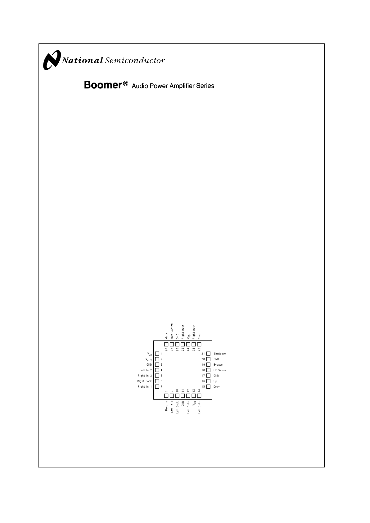
Connection Diagram
Boomer®is a registered trademark of NationalSemiconductor Corporation.
LLP Package
DS200104-35
Top View
Order Number LM4840LQ
See NS Package Number LQA028A for Exposed-DAP LLP
December 2001
LM4840 Stereo 2W Audio Power Amplifiers with Digital Volume Control and Input Mux
© 2001 National Semiconductor Corporation DS200104 www.national.com
Page 2
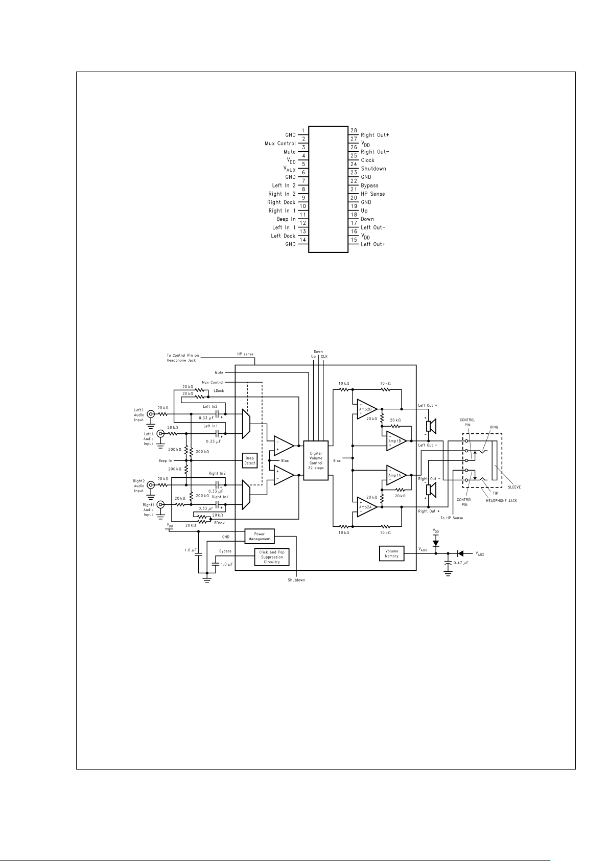
Connection Diagram (Continued)
Block Diagram
TSSOP Package
DS200104-2
Top View
Order Number LM4840MT
See NS Package Number MTC28 for TSSOP
Order Number LM4840MH
See NS Package Number MXA28A for Exposed-DAP TSSOP
DS200104-1
FIGURE 1. LM4840 Block Diagram
LM4840
www.national.com 2
Page 3
Absolute Maximum Ratings (Note 10)
If Military/Aerospace specified devices are required,
please contact the National Semiconductor Sales Office/
Distributors for availability and specifications.
Supply Voltage 6.0V
Storage Temperature -65˚C to +150˚C
Input Voltage −0.3V to V
DD
+0.3V
Power Dissipation Internally limited
ESD Susceptibility (Note 12) 2000V
ESD Susceptibility (Note 13) 200V
Junction Temperature 150˚C
Soldering Information
Small Outline Package
Vapor Phase (60 sec.) 215˚C
Infrared (15 sec.) 220˚C
See AN-450 “Surface Mounting and their Effects on
Product Reliability” for other methods of soldering
surface mount devices.
See AN-1187 “Leadless Leadframe Package” for
detailed information on usage of LLP devices.
θ
JC
(typ)—LQA028A (Note
16)
3˚C/W
θ
JA
(typ)—LQA028A (Note
16)
42˚C/W
θ
JC
(typ)—MTC28 20˚C/W
θ
JA
(typ)—MTC28 80˚C/W
θ
JC
(typ)—MXA28A 2˚C/W
θ
JA
(typ)—MXA28A (Note 4) 41˚C/W
θ
JA
(typ)—MXA28A (Note 3) 54˚C/W
θ
JA
(typ)—MXA28A (Note 5) 59˚C/W
θ
JA
(typ)—MXA28A (Note 6) 93˚C/W
Operating Ratings
Temperature Range
T
MIN
≤ TA≤T
MAX
−40˚C ≤TA ≤ 85˚C
Supply Voltage 2.7V≤ V
DD
≤ 5.5V
Electrical Characteristics for Entire IC
(Notes 7, 10)
The following specifications apply for V
DD
= 5V unless otherwise noted. Limits apply for TA= 25˚C.
Symbol Parameter Conditions
LM4840
Units
(Limits)
Typical
(Note 14)
Limit
(Note 15)
V
DD
Supply Voltage 2.7 V (min)
5.5 V (max)
I
DD
Quiescent Power Supply Current VIN= 0V, IO= 0A 12 30 mA (max)
I
SD
Shutdown Current V
SHUTDOWN
=V
DD
0.7 2.0 µA (max)
V
IH
Headphone Sense High Input Voltage 4 V (min)
V
IL
Headphone Sense Low Input Voltage 0.8 V (max)
Electrical Characteristics for Volume Attenuators
(Notes 7, 10)
The following specifications apply for V
DD
= 5V. Limits apply for TA= 25˚C.
Symbol Parameter Conditions
LM4840
Units
(Limits)
Typical
(Note 14)
Limit
(Note 15)
C
RANGE
Attenuator Range Gain with Digital Volume Max 0
±
0.5 dB (max)
Attenuation with Digital Volume Min -81 -75 dB (min)
A
M
Mute Attenuation V
MUTE=VDD
, Bridged Mode -88 -78 dB (min)
V
MUTE=VDD
, Single-Ended Mode -88 -78 dB (min)
Electrical Characteristics for Single-Ended Mode Operation
(Notes 7, 10)
The following specifications apply for V
DD
= 5V. Limits apply for TA= 25˚C.
Symbol Parameter Conditions
LM4840
Units
(Limits)
Typical
(Note 14)
Limit
(Note 15)
P
O
Output Power THD = 1.0%; f = 1kHz; RL=32Ω 85 mW
THD=10%;f=1kHz; R
L
=32Ω 95 mW
LM4840
www.national.com3
Page 4
Electrical Characteristics for Single-Ended Mode Operation (Continued)
(Notes 7, 10)
The following specifications apply for V
DD
= 5V. Limits apply for TA= 25˚C.
Symbol Parameter Conditions
LM4840
Units
(Limits)
Typical
(Note 14)
Limit
(Note 15)
THD+N Total Harmonic Distortion+Noise V
OUT
=1V
RMS
, f=1kHz, RL= 10kΩ,
A
VD
=1
0.065 %
PSRR Power Supply Rejection Ratio C
B
= 1.0 µF, f =120 Hz,
V
RIPPLE
= 200 mVrms
58 dB
SNR Signal to Noise Ratio P
OUT
=75 mW, RL=32Ω, A-Wtd
Filter
102 dB
X
talk
Channel Separation f=1kHz, CB= 1.0 µF 65 dB
Electrical Characteristics for Bridged Mode Operation
(Notes 7, 10)
The following specifications apply for V
DD
= 5V, unless otherwise noted. Limits apply for TA= 25˚C.
Symbol Parameter Conditions
LM4840
Units
(Limits)
Typical
(Note 14)
Limit
(Note 15)
V
OS
Output Offset Voltage VIN= 0V, No Load 5 50 mV (max)
P
O
Output Power THD+N=1.0%; f=1kHz; RL=3Ω
(Note 8)
2.2 W
THD+N=1.0%; f=1kHz; R
L
=4Ω
(Note 9)
2W
THD = 1.5% (max);f = 1 kHz;
R
L
=8Ω
1.1 1.0 W (min)
THD+N = 10%;f = 1 kHz; R
L
=8Ω 1.5 W
THD+N Total Harmonic Distortion+Noise P
O
= 1W, 20 Hz<f<20 kHz,
R
L
=8Ω,AVD=2
0.3 %
P
O
= 340 mW, RL=32Ω 1.0 %
PSRR Power Supply Rejection Ratio C
B
= 1.0 µF, f = 120 Hz,
V
RIPPLE
= 200 mVrms; RL=8Ω
74 dB
SNR Signal to Noise Ratio V
DD
= 5V, P
OUT
= 1.1W, RL=8Ω,
A-Wtd Filter
93 dB
X
talk
Channel Separation f=1kHz, CB= 1.0 µF 70 dB
Note 3: The θJAgiven is for an MXA28A package whose exposed-DAP is soldered to an exposed 2in2piece of 1 ounce printed circuit board copper.
Note 4: The θ
JA
given is for an MXA28A package whose exposed-DAP is soldered to a 2in2piece of 1 ounce printed circuit board copper on a bottom side layer
through 21 8mil vias.
Note 5: The θ
JA
given is for an MXA28A package whose exposed-DAP is soldered to an exposed 1in2piece of 1 ounce printed circuit board copper.
Note 6: The θ
JA
given is for an MXA28A package whose exposed-DAP is not soldered to any copper.
Note 7: All voltages are measured with respect to the ground pins, unless otherwise specified. All specifications are tested using the typical application as shown
in
Figure 1
.
Note 8: When driving 3Ω loads from a 5V supply the LM4840LQ and LM4840MH must be mounted to the circuit board and forced-air cooled.
Note 9: When driving 4Ω loads from a 5V supply the LM4840LQ and LM4840MH must be mounted to the circuit board.
Note 10:
Absolute Maximum Ratings
indicate limits beyond which damage to the device may occur.
Operating Ratings
indicate conditions for which the device is
functional, but do not guarantee specific performance limits.
Electrical Characteristics
state DC and AC electrical specifications under particular test conditions which
guarantee specific performance limits. This assumes that the device is within the Operating Ratings. Marshall Chiu feels there are better ways to obtain ’More
Wattage in the Cottage.’ Specifications are not guaranteed for parameters where no limit is given, however, the typical value is a good indication of device
performance.
Note 11: The maximum power dissipation must be derated at elevated temperatures and is dictated by T
JMAX
, θJA, and the ambient temperature TA. The maximum
allowable power dissipation is P
DMAX
=(T
JMAX−TA
)/θJA. For the LM4840LQ and LM4840MT, T
JMAX
= 150˚C, and the typical junction-to-ambient thermal
resistance, when board mounted, is 80˚C/W for the MTC28 package and 42˚C/W for the LM4840LQ package.
Note 12: Human body model, 100 pF discharged through a 1.5 kΩ resistor.
Note 13: Machine Model, 220 pF–240 pF discharged through all pins.
Note 14: Typicals are specified at 25˚C and represent the parametric norm.
Note 15: Datasheet min/max specification limits are guaranteed by design, test, or statistical analysis.
Note 16: Number given is for an LQA028A package whose exposed-DAP is soldered to an exposed 2.5in
2
piece of 1 ounce PCB copper.
LM4840
www.national.com 4
Page 5
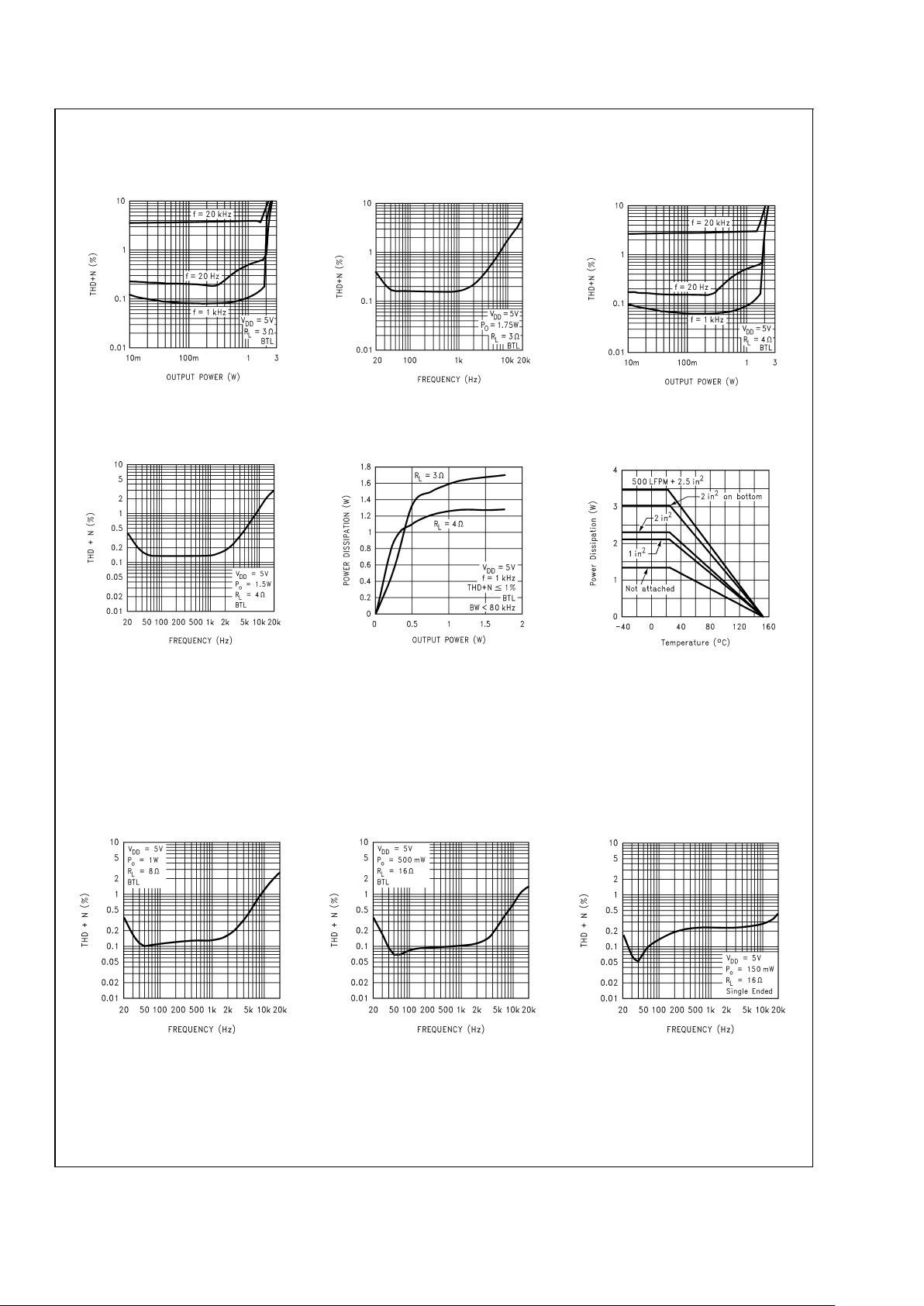
MH and LQ Specific Characteristics
Note 17: These curves show the thermal dissipation ability of the LM4840MH at different ambient temperatures given these conditions:
500LFPM + 2in
2
: The part is soldered to a 2in2, 1 oz. copper plane with 500 linear feet per minute of forced-air flow across it.
2in
2
on bottom: The part is soldered to a 2in2, 1oz. copper plane that is on the bottom side of the PC board through 21 8 mil vias.
2in
2
: The part is soldered to a 2in2, 1oz. copper plane.
1in
2
: The part is soldered to a 1in2, 1oz. copper plane.
Not Attached: The part is not soldered down and is not forced-air cooled.
Typical Performance Characteristics
LM4840MH, LM4840LQ
THD+N vs Output Power
DS200104-70
LM4840MH, LM4840LQ
THD+N vs Frequency
DS200104-71
LM4840MH, LM4840LQ
THD+N vs Output Power
DS200104-72
LM4840MH, LM4840LQ
THD+N vs Frequency
DS200104-73
LM4840MH, LM4840LQ
Power Dissipation vs Output Power
DS200104-65
LM4840MH(Note 17)
Power Derating Curve
DS200104-64
THD+N vs Frequency
DS200104-57
THD+N vs Frequency
DS200104-58
THD+N vs Frequency
DS200104-14
LM4840
www.national.com5
Page 6
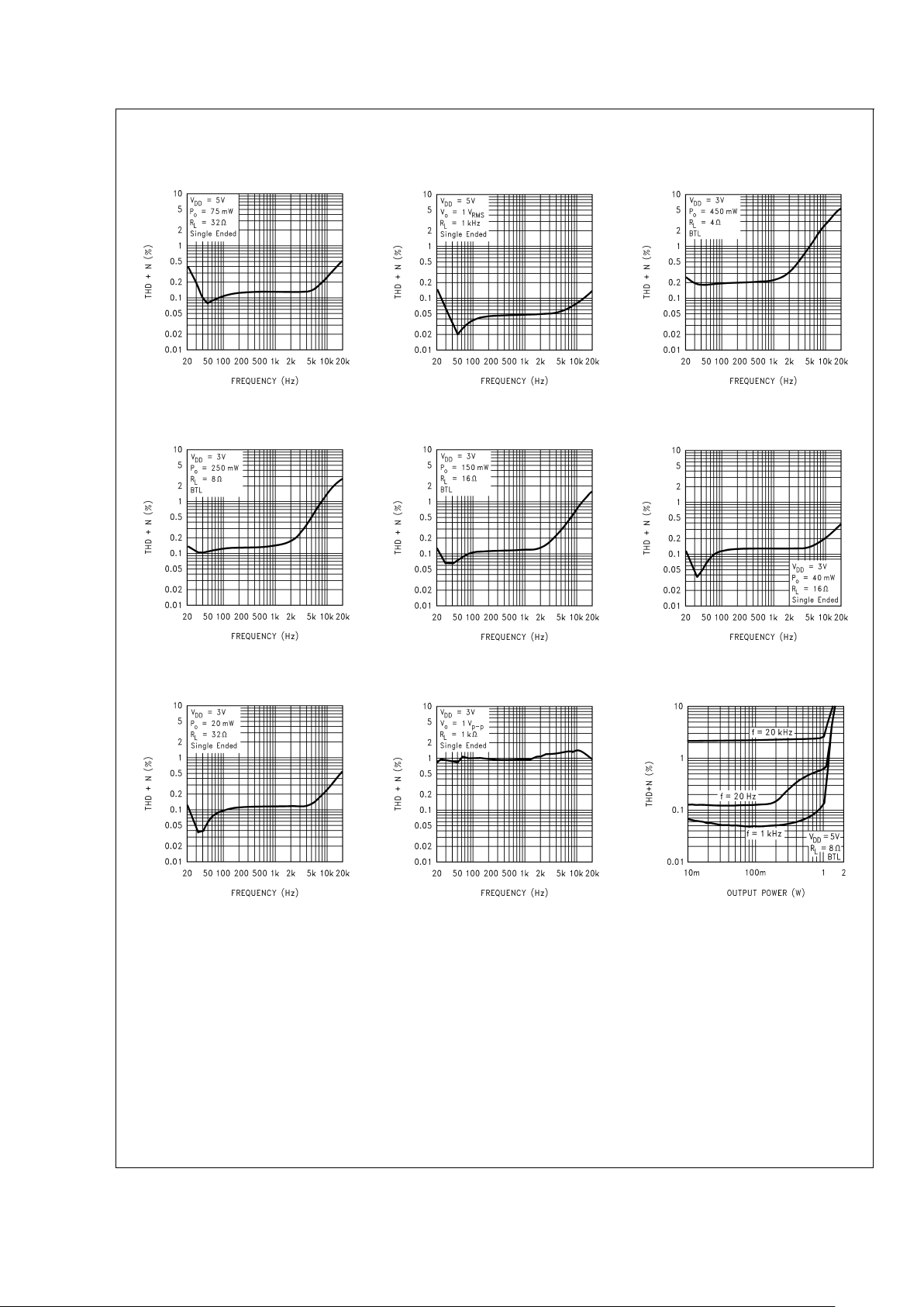
Typical Performance Characteristics (Continued)
THD+N vs Frequency
DS200104-15
THD+N vs Frequency
DS200104-16
THD+N vs Frequency
DS200104-17
THD+N vs Frequency
DS200104-18
THD+N vs Frequency
DS200104-19
THD+N vs Frequency
DS200104-20
THD+N vs Frequency
DS200104-21
THD+N vs Frequency
DS200104-22
THD+N vs Output Power
DS200104-24
LM4840
www.national.com 6
Page 7

Typical Performance Characteristics (Continued)
THD+N vs Output Power
DS200104-25
THD+N vs Output Power
DS200104-26
THD+N vs Output Power
DS200104-27
THD+N vs Output Power
DS200104-28
THD+N vs Output Power
DS200104-29
THD+N vs Output Power
DS200104-30
THD+N vs Output Power
DS200104-31
THD+N vs Output Power
DS200104-32
THD+N vs Output Power
DS200104-33
LM4840
www.national.com7
Page 8

Typical Performance Characteristics (Continued)
THD+N vs Output Power
DS200104-34
Output Power vs
Load Resistance
DS200104-62
Output Power vs
Load Resistance
DS200104-6
Output Power vs
Load Resistance
DS200104-7
Power Supply
Rejection Ratio
DS200104-38
Dropout Voltage
DS200104-53
Output Power vs
Load Resistance
DS200104-8
Noise Floor
DS200104-41
Noise Floor
DS200104-42
LM4840
www.national.com 8
Page 9

Typical Performance Characteristics (Continued)
Power Dissipation vs
Output Power
DS200104-51
Power Dissipation vs
Output Power
DS200104-52
Power Derating Curve
DS200104-63
Crosstalk
DS200104-49
Crosstalk
DS200104-50
Output Power
vs Supply voltage
DS200104-54
Output Power
vs Supply Voltage
DS200104-56
LM4840
www.national.com9
Page 10

Application Information
DIGITAL VOLUME CONTROL
The LM4840 features a digital volume control which consists
of the CLOCK, UP, and DOWN pins. An external clock may
be fed to the CLOCK pin, or, by connecting a capacitor from
the CLOCK pin to ground, the internal clock may be used.
The internal clock frequency with respect to this capacitor
value is determined from the following formula:
f
CLK
= (7.338 x 10⁻⁷)/C
When using an external clock, the clock is buffered and the
internal clock frequency is that of the external clock divided
by 2. Also, the maximum frequency should be kept below
100kHz.
Volume changes are then effected by toggling either the UP
or DOWN pins with a logic high. After a period of 4 clock
pulses with either the UP or DOWN pins held high, the
volume will change to the next specified step, either up or
down. Volume levels for each step vary and are specified in
Table 2. If either the UP or DOWN pin remains high after the
first volume transition the volume will change again, but this
time after 40 clock pulses. The next transition occurs at 20
clock pulses, then 12, then 8, and from then on 4 clock
pulses for each volume transtition. This cycle is shown in the
timing diagram shown in Figure 3. Releasing the held UP or
DOWN pin to ground at any time re-starts the cycle. This is
intended to provide the user with a volume control that
pauses briefly after initial application, then slowly increases
the rate of volume change as it is continuously applied.
If both the UP and DOWN pins are held high, no volume
change will occur. Trigger points for the UP and DOWN pins
are at 60% of V
DD
minimum for a logic high, and 20% of V
DD
maximum for a logic low. It is recommended, however, to
toggle UP and DOWN between V
DD
and GND for best
performance. When using an external clock, clock pulses
should be a minimum 0f 3V for a high and maximum of 0.9V
for a low when using a 5V supply. Again, pulsing an external
clock from V
DD
to GND ensures reliable performance. Following these guidelines the volume may then be changed
with a microcontroller or manually using switches.
MEMORY FUNCTION
The LM4840 features a volume memory that saves the last
volume setting when power is turned off. This requires that
an auxiliary power source be connected to V
AUX
through a
diode as shown in Figure 1. Connecting the circuit as shown
also provides that power to the V
AUX
pin is being drawn from
V
DD
when VDDis on and is greater than V
AUX.VAUX
must be
at a voltage of 2.3V or greater to maintain volume memory
when V
DD
is absent. This feature is intended for such appli-
cations as laptop computers, where V
DD
is the system power
and V
AUX
is connected to the real time clock battery. The
default volume setting for the LM4840 is -10dB in BTL mode,
and -16dB in single-ended mode. This default setting is only
achieved on power up when both V
DD
and V
AUX
had both
been turned off, and the circuit had sufficient time to discharge (
<
500ms depending on capacitor value at V
AUX
).
ELIMINATING OUTPUT COUPLING CAPACITORS
Typical single-supply audio amplifiers that can switch between driving bridge-tied-load (BTL) speakers and
single-ended (SE) headphones use a coupling capacitor on
each SE output. This capacitor blocks the half-supply voltage to which the output amplifiers are typically biased and
couples the audio signal to the headphones. The signal
return to circuit ground is through the headphone jack’s
sleeve.
The LM4840 eliminates these coupling capacitors. Amp2A is
internally configured to apply V
DD
/2 to a stereo headphone
jack’s sleeve. This voltage matches the quiescent voltage
present on the Amp1A and Amp1B outputs that drive the
headphones. The headphones operate in a manner very
similar to a bridge-tied-load (BTL). The same DC voltage is
applied to both headphone speaker terminals. This results in
no net DC current flow through the speaker.AC current flows
through a headphone speaker as an audio signal’s output
amplitude increases on the speaker’s terminal.
When operating as a headphone amplifier, the headphone
jack sleeve is not connected to circuit ground. Using the
headphone output jack as a line-level output will place the
LM4840’s one-half supply voltage on a plug’s sleeve connection. Driving a portable notebook computer or
audio-visual display equipment is possible. This presents no
difficulty when the external equipment uses capacitively
coupled inputs. For the very small minority of equipment that
is DC-coupled, the LM4840 monitors the current supplied by
the amplifier that drives the headphone jack’s sleeve. If this
current exceeds 500mA
PK
, the amplifier is shutdown, protecting the LM4840 and the external equipment. For more
information, see the section titled ’Single-Ended Output
Power Performance and Measurement Considerations’.
EXPOSED-DAP MOUNTING CONSIDERATIONS
The LM4840’s exposed-DAP (die attach paddle) packages
(MH, LQ) provide a low thermal resistance between the die
and the PCB to which the part is mounted and soldered. This
allows rapid heat transfer from the die to the surrounding
PCB copper traces, ground plane and, finally, surrounding
air. The result is a low voltage audio power amplifier that
produces 2W at ≤ 1% THD with a 4Ω load. This high power
is achieved through careful consideration of necessary thermal design. Failing to optimize thermal design may compromise the LM4840’s high power performance and activate
unwanted, though necessary, thermal shutdown protection.
The MH and LQ packages must have their exposed DAPs
soldered to a grounded copper pad on the PCB. The DAP’s
PCB copper pad is connected to a large plane of continuous
unbroken copper. This plane forms a thermal mass and heat
sink and radiation area. Place the heat sink area on either
outside plane in the case of a two-sided PCB, or on an inner
layer of a board with more than two layers. Connect the DAP
copper pad to the inner layer or backside copper heat sink
area with 32(4x8) (MH ) or 6(3x2) (LQ) vias. The via diameter should be 0.012in–0.013inwith a 1.27mm pitch. Ensure
efficient thermal conductivity by plating-through and solderfilling the vias.
Best thermal performance is achieved with the largest practical copper heat sink area. If the heatsink and amplifier
share the same PCB layer, a nominal 2.5in
2
(min) area is
necessary for 5V operation with a 4Ω load. Heatsink areas
not placed on the same PCB layer as the should be 5in
2
(min) for the same supply voltage and load resistance. The
last two area recommendations apply for 25˚C ambient temperature. Increase the area to compensate for ambient temperatures above 25˚C. In systems using cooling fans, the
LM4840MH can take advantage of forced air cooling. With
an air flow rate of 450 linear-feet per minute and a 2.5in
2
exposed copper or 5.0in2inner layer copper plane heatsink,
the LM4840MH can continuously drive a 3Ω load to full
power. The LM4840LQ achieves the same output power
LM4840
www.national.com 10
Page 11

Application Information (Continued)
level without forced air cooling. In all circumstances and
conditions, the junction temperature must be held below
150˚C to prevent activating the LM4840’s thermal shutdown
protection. The LM4840’s power derating curve in the Typi-
cal Performance Characteristics shows the maximum
power dissipation versus temperature. Further detailed and
specific information concerning PCB layout, fabrication, and
mounting an LQ (LLP) package is available in National
Semiconductor’s AN1187.
POWER DISSIPATION
Power dissipation is a major concern when using any power
amplifier and must be thoroughly understood to ensure a
successful design. Equation 1 states the maximum power
dissipation point for a single-ended amplifier operating at a
given supply voltage and driving a specified load.
P
DMAX
=(VDD)2/(2π2RL) (1)
However, a direct consequence of the increased power delivered to the load by a bridged amplifier is an increase in
internal power dissipation. Equation 2 states the maximum
power dissipation point for a bridged amplifier operating at a
given supply voltage and driving a specified load.
P
DMAX
= 4(VDD)2/(2π2RL) (2)
Since theLM4840 is a stereo power amplifier, the maximum
internal power dissipation is two times that of Equation 1 or
Equation 2 depending on the mode of operation. Even with
the power dissipation of the stereo amplifiers, the LM4840
does not require heatsinking. The power dissipation from the
amplifiers, must not be greater than the package power
dissipation that results from Equation 3:
P
DMAX
=(T
JMAX−TA
)/ θJA(3)
For the LM4840 TSSOP package, θ
JA
= 80˚C/W and T
JMAX
= 150˚C. Depending on the ambient temperature, TA,ofthe
system surroundings, Equation 3 can be used to find the
maximum internal power dissipation supported by the IC
packaging. If the result of Equation 1 and 2 is greater than
that of Equation 3, then either the supply voltage must be
decreased, the load impedance increased, or the ambient
temperature reduced. For the typical application of a 5V
power supply, with an 8Ω bridged loads, the maximum ambient temperature possible without violating the maximum
junction temperature is approximately 48˚C provided that
device operation is around the maximum power dissipation
points. Power dissipation is a function of output power and
thus, if typical operation is not around the maximum power
dissipation point, the ambient temperature can be increased.
Refer to the Typical Performance Characteristics curves
for power dissipation information for different output powers.
LAYOUT
As stated in the Grounding section, placement of ground
return lines is imperative in maintaining the highest level of
system performance. It is not only important to route the
correct ground return lines together, but also to be aware of
where the ground return lines are routed with respect to each
other. The output load ground returns should be physically
located as far as possible from low signal level lines and their
ground return lines.
3Ω and 4Ω Layout Considerations
With low impedance loads, the output power at the loads is
heavily dependent on trace resistance from the output pins
of the LM4840. Traces from the output of the LM4840MH to
the load or load connectors should be as wide as practical.
Any resistance in the output traces will reduce the power
delivered to the load. For example, with a 4Ω load and 0.1Ω
of trace resistance in each output, output power at the load
drops from 2W to 1.8W.
Output power is also dependent on supply regulation. To
keep the supply voltage from sagging under full output conditions, the supply traces should be as wide as practical.
Grounding
In order to achieve the best possible performance, there are
certain grounding techniques to be followed. All input reference grounds should be tied with their respective source
grounds and brought back to the power supply ground separately from the output load ground returns. Bringing the
ground returns for the output loads back to the supply separately will keep large signal currents from interfering with the
stable AC input ground references. The exposed-DAP of the
LM4840MH package must be tied to ground.
POWER SUPPLY BYPASSING
As with any power amplifier, proper supply bypassing is
critical for low noise performance and high power supply
rejection. The capacitor location on both the bypass and
power supply pins should be as close to the device as
possible. The effect of a larger half supply bypass capacitor
is improved PSRR due to increased half-supply stability.
Typicalapplications employ a 5 volt regulator with 10 µF and
a 0.1 µF bypass capacitors which aid in supply stability, but
do not eliminate the need for bypassing the supply nodes of
the LM4840. The selection of bypass capacitors, especially
C
B
, is thus dependant upon desired PSRR requirements,
click and pop performance as explained in the section,
Proper Selection of External Components, system cost,
and size constraints. It is also recommended to decouple
each of the V
DD
pins with a 0.1µF capacitor to ground.
PROPER SELECTION OF EXTERNAL COMPONENTS
Proper selection of external components in applications using integrated power amplifiers is critical to optimize device
and system performance. While the LM4840 is tolerant of
external component combinations, consideration to component values must be used to maximize overall system quality.
The LM4840’s bridged amplifier should be used in low gain
configurations to minimize THD+N values, and maximize the
signal to noise ratio. Low gain configurations require large
input signals to obtain a given output power. Input signals
equal to or greater than 1Vrms are available from sources
such as audio codecs.
Besides gain, one of the major considerations is the closedloop bandwidth of the amplifier. To a large extent, the bandwidth is dictated by the choice of external components. Both
the input coupling capacitor, C
I
, and the output coupling
capacitor form first order high pass filters which limit low
frequency response given in Equations 4 and 5.
f
IC
= 1/(2πRiCi) (4)
f
OC
= 1/(2πRLCO) (5)
These values should be chosen based on required frequency response.
Selection of Input and Output Capacitor Size
Large input and output capacitors are both expensive and
space hungry for portable designs. Clearly, a certain sized
capacitor is needed to couple in low frequencies without
LM4840
www.national.com11
Page 12

Application Information (Continued)
severe attenuation. In many cases the speakers used in
portable systems, whether internal or external, have little
ability to reproduce signals below 100 Hz–150 Hz. In this
case, usinga large input or output capacitor may not increase system performance.
In addition to system cost and size, click and pop performance is effected by the size of the input coupling capacitor,
C
i
. A larger input coupling capacitor requires more charge to
reach its quiescent DC voltage (nominally 1/2 V
DD
.) This
charge comes from the output through the feedback and is
apt to create pops once the device is enabled. By minimizing
the capacitor size based on necessary low frequency response, turn-on pops can be minimized.
CLICK AND POP CIRCUITRY
The LM4840 contains circuitry to minimize turn-on transients
or “click and pops”. In this case, turn-on refers to either
power supply turn-on or the device coming out of shutdown
mode. When the device is turning on, the amplifiers are
internally muted. An internal current source ramps up the
voltage of the bypass pin. Both the inputs and outputs ideally
track the voltage at the bypass pin. The device will remain in
mute mode until the bypass pin has reached its half supply
voltage, 1/2 V
DD
. As soon as the bypass node is stable, the
device will become fully operational.
Although the bypass pin current source cannot be modified,
the size of the bypass capacitor, C
B
, can be changed to alter
the device turn-on time and the amount of “click and pop”. By
increasing C
B
, the amount of turn-on pop can be reduced.
However, the trade-off for using a larger bypass capacitor is
an increase in the turn-on time for the device. Reducing C
B
will decrease turn-on time and increase “click and pop”.
There is a linear relationship between the size of C
B
and the
turn-on time. Here are some typical turn-on times for different values of C
B
:
C
B
T
ON
0.01 µF 2 ms
0.1 µF 20 ms
0.22 µF 42 ms
0.47 µF 84 ms
1.0 µF 200 ms
4.7 µF 1sec
In order to eliminate “click and pop”, all capacitors must be
discharged before turn-on. Rapid on/off switching of the
device or shutdown function may cause the “click and pop”
circuitry to not operate fully, resulting in increased “click and
pop” noise.
DOCKING STATION
In an application such as a notebook computer, docking
station or line level outputs may be required. Pin 9 and Pin
13 can drive loads greater than 1kΩ rail to rail. These pins
are tied to the output of the input op-amp to drive powered
speakers and other high impedance loads. Output coupling
capacitors need to be placed in series with the load. The
recommended values of the capacitors are between 0.33µF
to 1.0µF with the positive side of the capacitors toward the
IC. The outputs of the docking station pins cannot be attenuated with the DC volume control. However the gain of the
outputs can be configured by adjusting the feedback and
input resistors for the input op-amp. The input op-amp is in
an inverting configuration where the gain is:
R
F/Ri
=-A
v
Note that by adjusting the gain of the input op-amp the
overall gain of the output amplifiers are also affected. Although the single ended outputs of the output amplifiers can
be used to drive line level outputs, it is recommended to use
Pins 9 and 13 to achieve better performance.
BEEP DETECT FUNCTION
The Beep Detect pin (Beep In) is a mono input that detects
the presence of a beep signal. When a signal greater than
2.5V
P-P
(or 1/2 VDD) is present at Beep In, the Beep Detect
circuitry will enable the bridged amplifiers. Beep In signals
less than 2.5V
P-P
(or 1/2 VDD) will not trigger the Beep
Detect circuitry. When triggered, the Beep Detect circuitry
will enable the bridged amplifiers regardless of the state of
the mute, mode, or HP sense pins. As shown in the Fig. 1, a
200kΩ resistor is placed in series with the input capacitor.
This 200kΩ resistor can be changed to vary the amplitude of
the beep in signal. Higher values of the resistor will reduce
the amplifier gain and attenuate the beep in signal. These
resistors are required in order for the beep signal to pass to
the output. The Beep Detect pin will not pass the beep signal
to the output. In cases where system beeps are required
when the system is in a suspended mode, the LM4840 must
be brought out of shutdown before the beep in signal is input.
SHUTDOWN FUNCTION
In order to reduce power consumption while not in use, the
LM4840 contains a shutdown pin to externally turn off the
bias circuitry. The LM4840 will shutdown when a logic high is
placed on the shutdown pin. The trigger point between a
logic low and logic high level is typically half supply. It is best
to switch between ground and the supply V
DD
to provide
maximum device performance. By switching the shutdown
pin to V
DD
, the LM4840 supply current draw will be minimized. While the device will be disabled with shutdown pin
voltages less than V
DD
, the idle current may be greater than
the typical value of 0.7 µA.The shutdown pin should not be
floated, since this may result in an unwanted shutdown
condition.
In many applications, a microcontroller or microprocessor
output is used to control the shutdown circuitry which provides a quick, smooth transition into shutdown. Another solution is to use a single-pole, single-throw switch in conjuction with an external pull-up resistor. When the switch is
closed,the shutdown pin is connected to ground and enables
the amplifier. If the switch is open, then the external pull-up
resistor will shutdown the LM4840. This scheme prevents
the shutdown pin from floating.
HP-IN FUNCTION
An internal pull−up circuit is connected to the HP−Sense
headphone amplifier control pin. When this pin is left unconnected, V
DD
is applied to the HP−Sense. This turns off
Amp2B and switches Amp2A’s input signal from an audio
signal to the V
DD
/2 voltage present on Bypass. The result is
muted bridge-connected loads. Quiescent current consumption is reduced when the IC is in this single−ended mode.
Figure 2
shows the implementation of the LM4840’s headphone control function. An internal comparator with a nominal 400mV offset monitors the signal present at the −OUTB
output. It compares this signal against the signal applied to
the HP−Sense pin. When these signals are equal, as is the
LM4840
www.national.com 12
Page 13

Application Information (Continued)
case when a BTL is connected to the amplifier, the comparator forces the LM4840 to maintain bridged−amplifier operation. When the HP−Sense pin is externally floated, such as
when headphones are connected to the jack shown in
Figure
2
, and internal pull−up forces VDDon the internal comparator’s HP−Sense inputs. This changes the comparator’s output state and enables the headphone function: it turns off
Amp2B, switches Amp2A’s input signal from an audio signal
to the V
DD
/2 voltage present on pin 14, and mutes the
bridge-connected loads. Amp1A and Amp1B drive the headphones.
Figure 2
also shows the suggested headphone jack electri-
cal connections. The jack is designed to mate with a
three−wire plug. The plug’s tip and ring should each carry
one of the two stereo output signals, whereas the sleeve
provides the return to Amp2A. A headphone jack with one
control pin contact is sufficient to drive the HP−Sense pin
when connecting headphones.
A switch can replace the headphone jack contact pin. When
a switch shorts the HP−Sense pin to V
DD
, bridge−connected
speakers are muted and Amp1A and Amp2A drive a pair of
headphones. When a switch shorts the HP−Sense pin to
GND, the LM4840 operates in bridge mode. If headphone
drive is not needed, short the HP−Sense pin to the −OUTB
pin.
DS200104-74
FIGURE 2. The ESDAxxxL provides additional ESD protection beyond the 8000V shown in the Absolute Maximum
Ratings for the AMP2A output
DS200104-75
FIGURE 3. Volume Control Timing Diagram
LM4840
www.national.com13
Page 14

Application Information (Continued)
Table 1: Logic Level Truth Table
SD BEEP
DETECT
MUTE HP
SENSE
MODE R- R+ L- L+
L L L L BTL SPK ON ON ON ON
L L L H HP ON ON (buffer) ON OFF
L L H L BTLSPK ON ON ON ON *Amps are muted
L L H H HP ON ON (buffer) ON OFF *Amps are muted
*Next four conditions, beep is detected; beep signal added to audio signal and bypasses volume control (unity)
L H L L BTL SPK ON ON ON ON
L H L H HP ON ON (buffer) ON ON
L H H L BTL SPK ON ON ON ON *Dual Mode
L H H H HP ON ON (buffer) ON ON *Dual Mode
*Next eight conditions turns off all amps
H L L L BTL SPK OFF OFF OFF OFF
H L L H HP OFF OFF OFF OFF
H L H L BTL SPK OFF OFF OFF OFF
H L H H HP OFF OFF OFF OFF
H H L L BTL SPK OFF OFF OFF OFF
H H L H HP OFF OFF OFF OFF
H H H L BTL SPK OFF OFF OFF OFF
H H H H HP OFF OFF OFF OFF
*Beepdetect signal overrides any mute. For example, if amp is muted and bpdetect is HIGH, then amp is no longer muted.
**Dual mode: When HP jack is inserted, load A (speaker corresponding to outputs A- and A+) is physically disconnected. Load
B remains connected; however, amp B+ is off and differentially there is no voltage across it. If a beep is detected (i.e. beepdetect
= HIGH), then summed signal (audio + beep signals) is heard in the headphones and on speaker B.
LM4840
www.national.com 14
Page 15

Application Information (Continued)
Table 2: LM4840 Volume Control Steps
Volume Step BTL (dB) SE (dB)
1 6.00 0.00
2 5.00 -1.00
3 4.00 -2.00
4 3.00 -3.00
5 2.00 -4.00
6 1.00 -5.00
7 0.00 -6.00
8 -2.00 -8.00
9 -4.00 -10.00
10 -6.00 -12.00
11 -8.00 -14.00
12 -10.00 -16.00
13 -12.00 -18.00
14 -14.00 -20.00
15 -16.00 -22.00
16 -18.00 -24.00
17 -20.00 -26.00
18 -21.90 -27.90
19 -24.00 -30.00
20 -26.10 -32.10
21 -28.10 -34.10
22 -29.90 -35.90
23 -32.70 -38.70
24 -36.00 -42.00
25 -38.80 -44.80
26 -41.30 -47.30
27 -44.90 -50.90
28 -50.90 -56.90
29 -56.90 -62.90
30 -62.90 -68.90
31 -70.90 -76.90
32 -70.90 -76.90
LM4840
www.national.com15
Page 16

Physical Dimensions inches (millimeters) unless otherwise noted
LLP Package
Order Number LM4840LQ
NS Package Number LQA028A for Exposed-DAP LLP
LM4840
www.national.com 16
Page 17

Physical Dimensions inches (millimeters) unless otherwise noted (Continued)
TSSOP Package
Order Number LM4840MT
NS Package Number MTC28 for TSSOP
LM4840
www.national.com17
Page 18

Physical Dimensions inches (millimeters) unless otherwise noted (Continued)
Exposed-DAP TSSOP Package
Order Number LM4840MH
NS Package Number MXA28A for Exposed-DAP TSSOP
LM4840
www.national.com 18
Page 19

Notes
LIFE SUPPORT POLICY
NATIONAL’S PRODUCTS ARE NOT AUTHORIZED FOR USE AS CRITICAL COMPONENTS IN LIFE SUPPORT
DEVICES OR SYSTEMS WITHOUT THE EXPRESS WRITTEN APPROVAL OF THE PRESIDENT AND GENERAL
COUNSEL OF NATIONAL SEMICONDUCTOR CORPORATION. As used herein:
1. Life support devices or systems are devices or
systems which, (a) are intended for surgical implant
into the body, or (b) support or sustain life, and
whose failure to perform when properly used in
accordance with instructions for use provided in the
labeling, can be reasonably expected to result in a
significant injury to the user.
2. A critical component is any component of a life
support device or system whose failure to perform
can be reasonably expected to cause the failure of
the life support device or system, or to affect its
safety or effectiveness.
National Semiconductor
Corporation
Americas
Email: support@nsc.com
National Semiconductor
Europe
Fax: +49 (0) 180-530 85 86
Email: europe.support@nsc.com
Deutsch Tel: +49 (0) 69 9508 6208
English Tel: +44 (0) 870 24 0 2171
Français Tel: +33 (0) 1 41 91 8790
National Semiconductor
Asia Pacific Customer
Response Group
Tel: 65-2544466
Fax: 65-2504466
Email: ap.support@nsc.com
National Semiconductor
Japan Ltd.
Tel: 81-3-5639-7560
Fax: 81-3-5639-7507
www.national.com
LM4840 Stereo 2W Audio Power Amplifiers with Digital Volume Control and Input Mux
National does not assume any responsibility for use of any circuitry described, no circuit patent licenses are implied and National reserves the right at any time without notice to change said circuitry and specifications.
 Loading...