

Page 1
LM4838
Stereo 2W Audio Power Amplifiers
with DC Volume Control and Selectable Gain
General Description
The LM4838 is a monolithic integrated circuit that provides
DC volume control, and stereo bridged audio power amplifiers capable of producing 2W into 4Ω (Note 1) with less than
1.0% THD or 2.2W into 3Ω (Note 2) with less than 1.0%
THD.
Boomer
®
audio integrated circuits were designed specifically
to provide high quality audio while requiring a minimum
amount of external components. The LM4838 incorporates a
DC volume control, stereo bridged audio power amplifiers
and a selectable gain or bass boost, making it optimally
suited for multimedia monitors, portable radios, desktop, and
portable computer applications.
The LM4838 features an externally controlled, low-power
consumption shutdown mode, and both a power amplifier
and headphone mute for maximum system flexibility and
performance.
Note 1: When properly mounted to the circuit board, the LM4838LQ and
LM4838MTE will deliver 2W into 4Ω. The LM4838MT and LM4838ITL will
deliver 1.1W into 8Ω. See Application Information section Exposed-DAP
package PCB Mounting Considerations for more information.
Note 2: An LM4838LQ and LM4838MTE that have been properly mounted
to the circuit board and forced-air cooled will deliver 2.2W into 3Ω.
Key Specifications
n POat 1% THD+N
n into 3Ω (LQ & MTE) 2.2W (typ)
n into 4Ω (LQ & MTE) 2.0W (typ)
n into 8Ω (MT, MTE, ITL, & LQ) 1.1W (typ)
n Single-ended mode - THD+N at 85mW into
32Ω 1.0%(typ)
n Shutdown current 0.7µA (typ)
Features
n DC Volume Control Interface
n System Beep Detect
n Stereo switchable bridged/single-ended power amplifiers
n Selectable internal/external gain and bass boost
n “Click and pop” suppression circuitry
n Thermal shutdown protection circuitry
Applications
n Portable and Desktop Computers
n Multimedia Monitors
n Portable Radios, PDAs, and Portable TVs
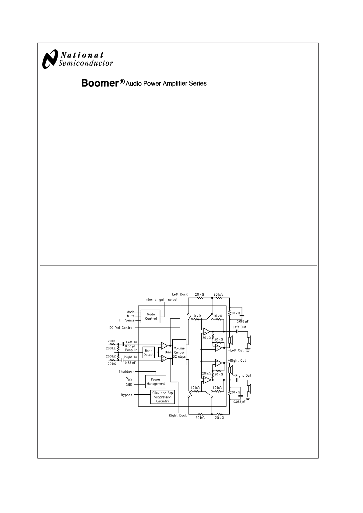
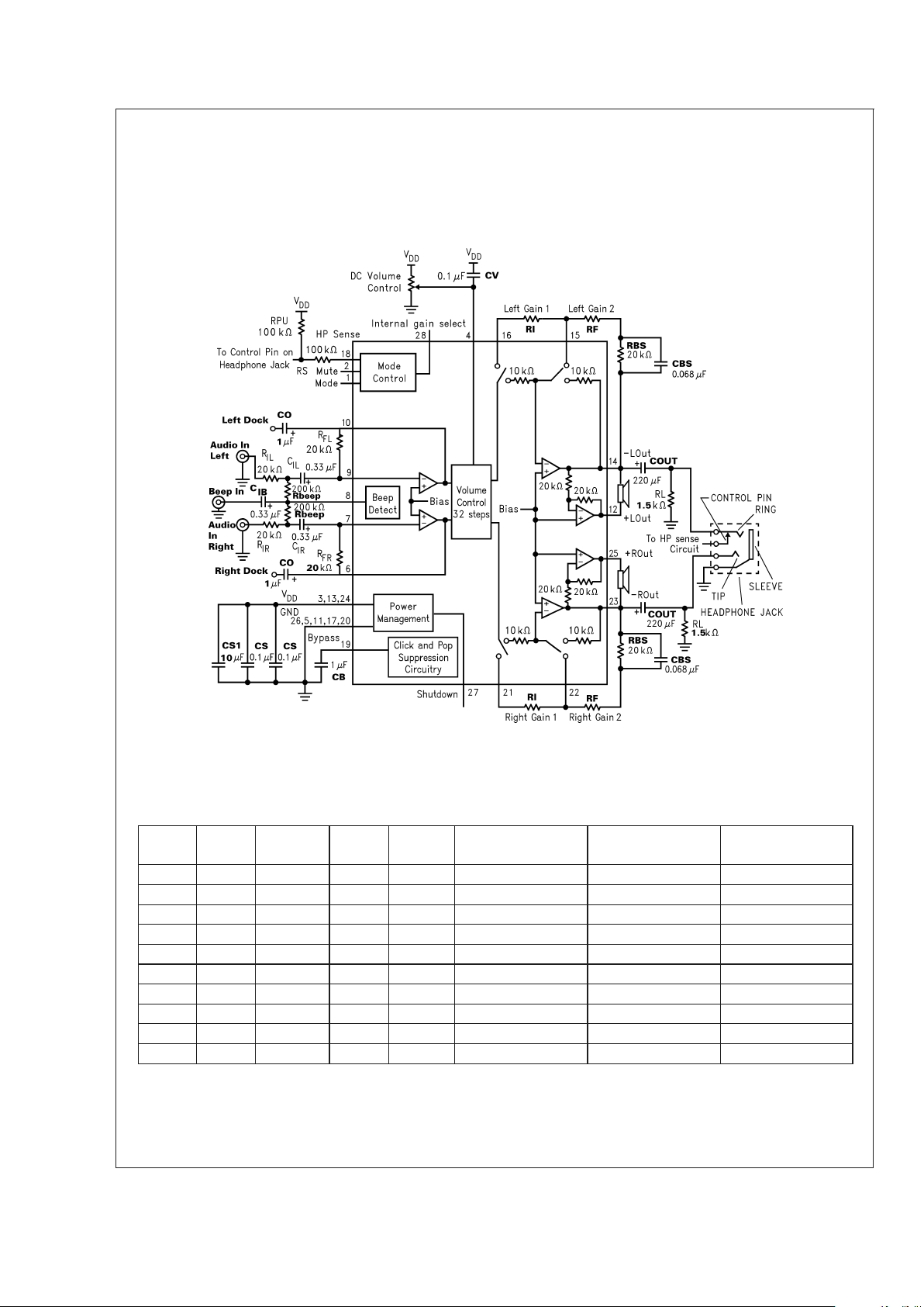
Block Diagram
Boomer®is a registered trademark of NationalSemiconductor Corporation.
20013301
FIGURE 1. LM4838 Block Diagram
January 2003
LM4838 Stereo 2W Audio Power Amplifiers with DC Volume Control and Selectable Gain
© 2003 National Semiconductor Corporation DS200133 www.national.com
Page 2
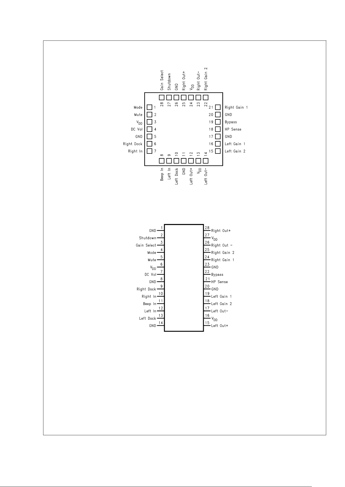
Connection Diagrams
LLP Package
20013335
Top View
Order Number LM4838LQ
See NS Package Number LQA028AA for Exposed-DAP LLP
TSSOP Package
20013302
Top View
Order Number LM4838MT
See NS Package Number MTC28 for TSSOP
Order Number LM4838MTE
See NS Package Number MXA28A for Exposed-DAP TSSOP
LM4838
www.national.com 2
Page 3
Connection Diagrams (Continued)
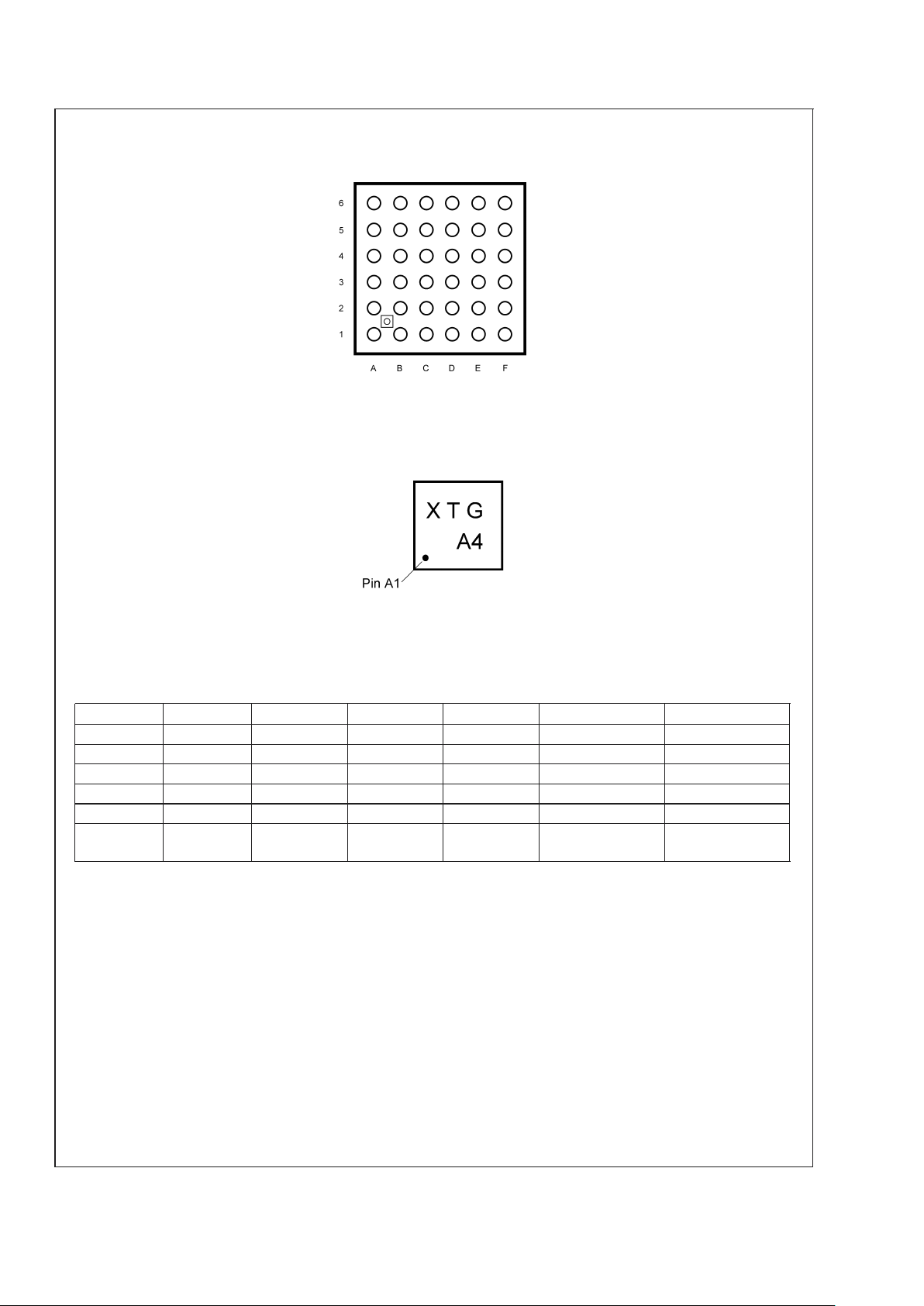
36 Bump micro SMD
20013388
Top View
Order Number LM4838ITL, LM4838ITLX
See NS Package Number TLA36AAA
micro SMD Marking
20013387
Top View
X - Date Code
T - Die Traceability
G - Boomer Family
A4 - LM4838ITL
6 NC Right Out - V
DD
Right Out + GND NC
5 GND Right Gain 2 Right Gain 1 Gain Select Shutdown Mode
4 Bypass NC NC DC Vol Mute V
DD
3 HP Sense NC NC Beep In Right Dock GND
2 GND Left Gain 2 Left Gain 1 Left In Left Dock Right In
1 NC Left Out - V
DD
Left Out + GND NC
Pin
Designator
AB C D E F
LM4838
www.national.com3
Page 4
Absolute Maximum Ratings (Note 10)
If Military/Aerospace specified devices are required,
please contact the National Semiconductor Sales Office/
Distributors for availability and specifications.
Supply Voltage 6.0V
Storage Temperature -65˚C to +150˚C
Input Voltage −0.3V to V
DD
+0.3V
Power Dissipation (Note 11) Internally limited
ESD Susceptibility (Note 12) 2000V
ESD Susceptibility (Note 13) 200V
Junction Temperature 150˚C
Soldering Information
Small Outline Package
Vapor Phase (60 sec.) 215˚C
Infrared (15 sec.) 220˚C
See AN-450 “Surface Mounting and their Effects on
Product Reliability” for other methods of soldering surface
mount devices.
θ
JC
(typ) —LQA028AA 3˚C/W
θ
JA
(typ) —LQA028AA 42˚C/W
θ
JC
(typ) —MTC28 20˚C/W
θ
JA
(typ) —MTC28 80˚C/W
θ
JC
(typ) —MXA28A 2˚C/W
θ
JA
(typ) —MXA28A (exposed
DAP) (Note 4)
41˚C/W
θ
JA
(typ) —MXA28A (exposed
DAP) (Note 3)
54˚C/W
θ
JA
(typ) —MXA28A (exposed
DAP) (Note 5)
59˚C/W
θ
JA
(typ) —MXA28A (exposed
DAP) (Note 6)
93˚C/W
θJA(typ) —ITL36AAA 100˚C/W
θ
JC
(typ) —ITL36AAA (Note 16) 65˚C/W
Operating Ratings
Temperature Range
T
MIN
≤ TA≤T
MAX
−40˚C ≤TA ≤ 85˚C
Supply Voltage 2.7V≤ V
DD
≤ 5.5V
Electrical Characteristics for Entire IC (Notes 7, 10)
The following specifications apply for VDD= 5V unless otherwise noted. Limits apply for TA= 25˚C.
Symbol Parameter Conditions
LM4838
Units
(Limits)
Typical
(Note 14)
Limit
(Note 15)
V
DD
Supply Voltage 2.7 V (min)
5.5 V (max)
I
DD
Quiescent Power Supply Current VIN= 0V, IO= 0A 15 30 mA (max)
I
SD
Shutdown Current V
shutdown
=V
DD
0.7 2.0 µA (max)
V
IH
Headphone Sense High Input Voltage 4 V (min)
V
IL
Headphone Sense Low Input Voltage 0.8 V (max)
Electrical Characteristics for Volume Attenuators (Notes 7, 10)
The following specifications apply for VDD= 5V. Limits apply for TA= 25˚C.
Symbol Parameter Conditions
LM4838
Units
(Limits)
Typical
(Note 14)
Limit
(Note 15)
C
RANGE
Attenuator Range Gain with V
DCVol
= 5V, No Load
±
0.75 dB (max)
Attenuation with V
DCVol
= 0V (BM &
SE)
-75 dB (min)
A
M
Mute Attenuation V
mute
= 5V, Bridged Mode (BM) -78 dB (min)
V
mute
= 5V, Single-Ended Mode (SE) -78 dB (min)
Electrical Characteristics for Single-Ended Mode Operation (Notes 7, 10)
The following specifications apply for VDD= 5V. Limits apply for TA= 25˚C.
Symbol Parameter Conditions
LM4838
Units
(Limits)
Typical
(Note 14)
Limit
(Note 15)
P
O
Output Power THD = 1.0%; f = 1kHz; RL=32Ω 85 mW
THD=10%;f=1kHz; R
L
=32Ω 95 mW
LM4838
www.national.com 4
Page 5
Electrical Characteristics for Single-Ended Mode Operation (Notes 7,
10) (Continued)
The following specifications apply for VDD= 5V. Limits apply for TA= 25˚C.
Symbol Parameter Conditions
LM4838
Units
(Limits)
Typical
(Note 14)
Limit
(Note 15)
THD+N Total Harmonic Distortion+Noise V
OUT
=1V
RMS
, f=1kHz, RL= 10kΩ,
A
VD
=1
0.065 %
PSRR Power Supply Rejection Ratio C
B
= 1.0 µF, f =120 Hz,
V
RIPPLE
= 200 mVrms
58 dB
SNR Signal to Noise Ratio P
OUT
=75 mW, RL=32Ω, A-Wtd
Filter
102 dB
X
talk
Channel Separation f=1kHz, CB= 1.0 µF 65 dB
Electrical Characteristics for Bridged Mode Operation (Notes 7, 10)
The following specifications apply for VDD= 5V, unless otherwise noted. Limits apply for TA= 25˚C.
Symbol Parameter Conditions
LM4838
Units
(Limits)
Typical
(Note 14)
Limit
(Note 15)
V
OS
Output Offset Voltage VIN= 0V, No Load 5
±
50 mV (max)
P
O
Output Power THD+N=1.0%; f=1kHz; RL=3Ω
(Note 8)
2.2 W
THD+N=1.0%; f=1kHz; RL=4Ω
(Note 9)
2W
THD = 1% (max);f = 1 kHz;
R
L
=8Ω
1.1 1.0 W (min)
THD+N = 10%;f = 1 kHz; R
L
=8Ω 1.5 W
THD+N Total Harmonic Distortion+Noise P
O
= 1W, 20 Hz<f<20 kHz,
R
L
=8Ω,AVD=2
0.3 %
P
O
= 340 mW, RL=32Ω 1.0 %
PSRR Power Supply Rejection Ratio C
B
= 1.0 µF, f = 120 Hz,
V
RIPPLE
= 200 mVrms; RL=8Ω
74 dB
SNR Signal to Noise Ratio V
DD
= 5V, P
OUT
= 1.1W, RL=8Ω,
A-Wtd Filter
93 dB
X
talk
Channel Separation f=1kHz, CB= 1.0 µF 70 dB
Note 3: The θJAgiven is for an MXA28A package whose exposed-DAP is soldered to an exposed 2in2piece of 1 ounce printed circuit board copper.
Note 4: The θ
JA
given is for an MXA28A package whose exposed-DAP is soldered to a 2in2piece of 1 ounce printed circuit board copper on a bottom side layer
through 21 8mil vias.
Note 5: The θ
JA
given is for an MXA28A package whose exposed-DAP is soldered to an exposed 1in2piece of 1 ounce printed circuit board copper.
Note 6: The θ
JA
given is for an MXA28A package whose exposed-DAP is not soldered to any copper.
Note 7: All voltages are measured with respect to the ground pins, unless otherwise specified. All specifications are tested using the typical application as shown
in Figure 1.
Note 8: When driving 3Ω loads from a 5V supply the LM4838LQ, LM4838ITL and LM4838MTE must be mounted to the circuit board and forced-air cooled.
Note 9: When driving 4Ω loads from a 5V supply the LM4838LQ, LM4838ITL and LM4838MTE must be mounted to the circuit board.
Note 10: Absolute Maximum Ratings indicate limits beyond which damage to the device may occur. Operating Ratings indicate conditions for which the device is
functional, but do not guarantee specific performance limits. Electrical Characteristics state DC and AC electrical specifications under particular test conditions which
guarantee specific performance limits. This assumes that the device is within the Operating Ratings. Specifications are not guaranteed for parameters where no limit
is given, however, the typical value is a good indication of device performance.
Note 11: The maximum power dissipation must be derated at elevated temperatures and is dictated by T
JMAX
, θJA, and the ambient temperature TA. The maximum
allowable power dissipation is P
DMAX
=(T
JMAX−TA
)/θJA. For the LM4838, T
JMAX
= 150˚C, and the typical junction-to-ambient thermal resistance for each package
can be found in the Absolute Maximum Ratings section above.
Note 12: Human body model, 100 pF discharged through a 1.5 kΩ resistor.
Note 13: Machine Model, 220 pF– 240 pF discharged through all pins.
Note 14: Typicals are measured at 25˚C and represent the parametric norm.
Note 15: Limits are guaranteed to National’s AOQL ( Average Outgoing Quality Level). Datasheet min/max specification limits are guaranteed by design, test, or
statistical analysis.
LM4838
www.national.com5
Page 6
Electrical Characteristics for Bridged Mode Operation (Notes 7, 10) (Continued)
Note 16: All bumps have the same thermal resistance and contribute equally when used to lower thermal resistance. The LM4838ITL demo board (views featured
in the Application Information section) is a four layer board with two inner layers. The second inner layer is a V
DD
plane with the bottom outside layer a GND plane.
The planes measure 1,900mils x 1,750mils (48.26mm x 44.45mm) and aid in spreading heat due to power dissipation within the IC.
Typical Application
Truth Table for Logic Inputs
(Note 17)
Gain
Sel
Mode Headphone
Sense
Mute Shutdown Output Stage Set To DC Volume Output Stage
Configuration
0 0 0 0 0 Internal Gain Fixed BTL
0 0 1 0 0 Internal Gain Fixed SE
0 1 0 0 0 Internal Gain Adjustable BTL
0 1 1 0 0 Internal Gain Adjustable SE
1 0 0 0 0 External Gain Fixed BTL
1 0 1 0 0 External Gain Fixed SE
1 1 0 0 0 External Gain Adjustable BTL
1 1 1 0 0 External Gain Adjustable SE
X X X 1 0 Muted X Muted
X X X X 1 Shutdown X X
Note 17: If system beep is detected on the Beep In pin, the system beep will be passed through the bridged amplifier regardless of the logic of the Mute and HP
sense pins.
20013303
FIGURE 2. Typical Application Circuit ( LQ Package Pinout )
LM4838
www.national.com 6
Page 7
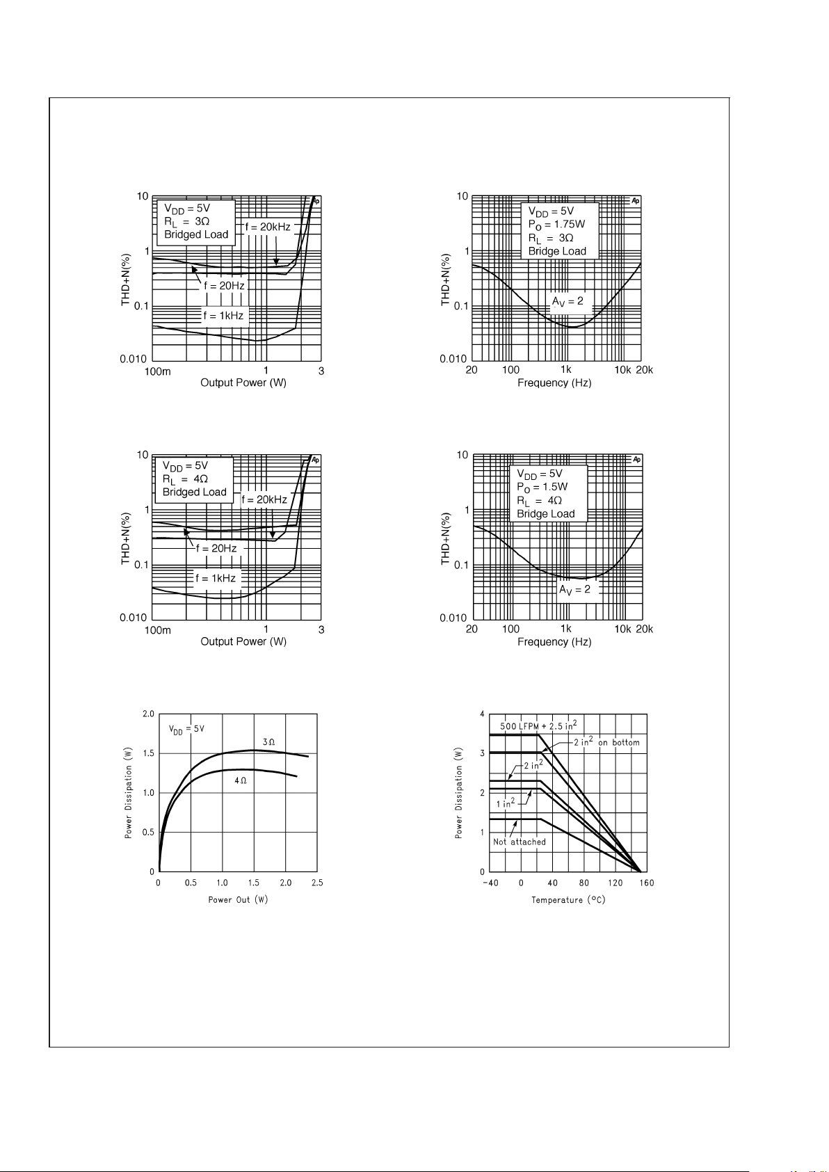
Typical Performance Characteristics
MTE Specific Characteristics
LM4838MTE
THD+N vs Output Power
LM4838MTE
THD+N vs Frequency
20013370
20013371
LM4838MTE
THD+N vs Output Power
LM4838MTE
THD+N vs Frequency
20013372
20013373
LM4838MTE
Power Dissipation vs Output Power
LM4838MTE (Note 18)
Power Derating Curve
20013365
20013364
Note 18: These curves show the thermal dissipation ability of the LM4838MTE at different ambient temperatures given these conditions:
500LFPM + 2in
2
: The part is soldered to a 2in2, 1 oz. copper plane with 500 linear feet per minute of forced-air flow across it.
2in
2
on bottom: The part is soldered to a 2in2, 1oz. copper plane that is on the bottom side of the PC board through 21 8 mil vias.
2in
2
: The part is soldered to a 2in2, 1oz. copper plane.
1in
2
: The part is soldered to a 1in2, 1oz. copper plane.
Not Attached: The part is not soldered down and is not forced-air cooled.
LM4838
www.national.com7
Page 8
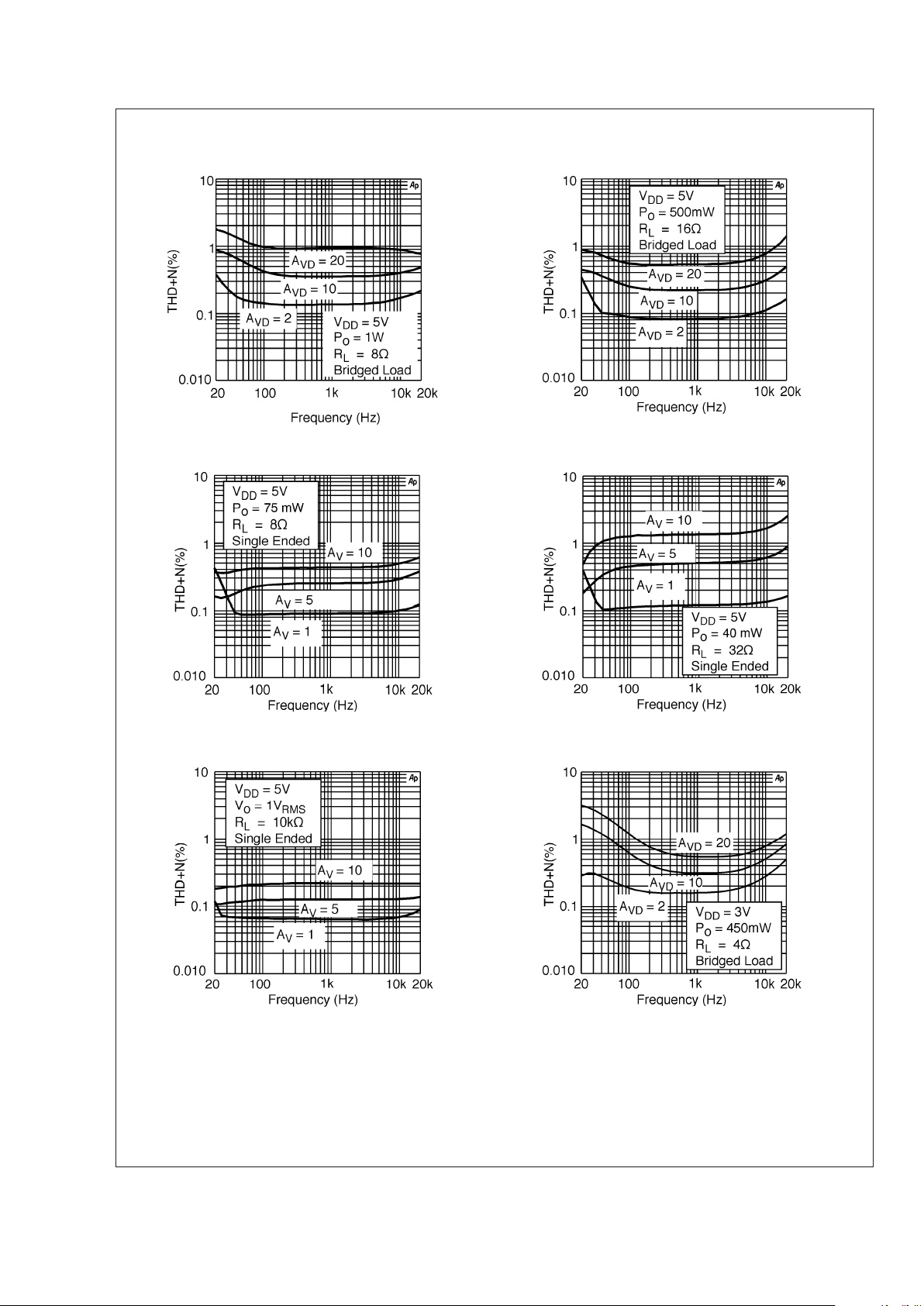
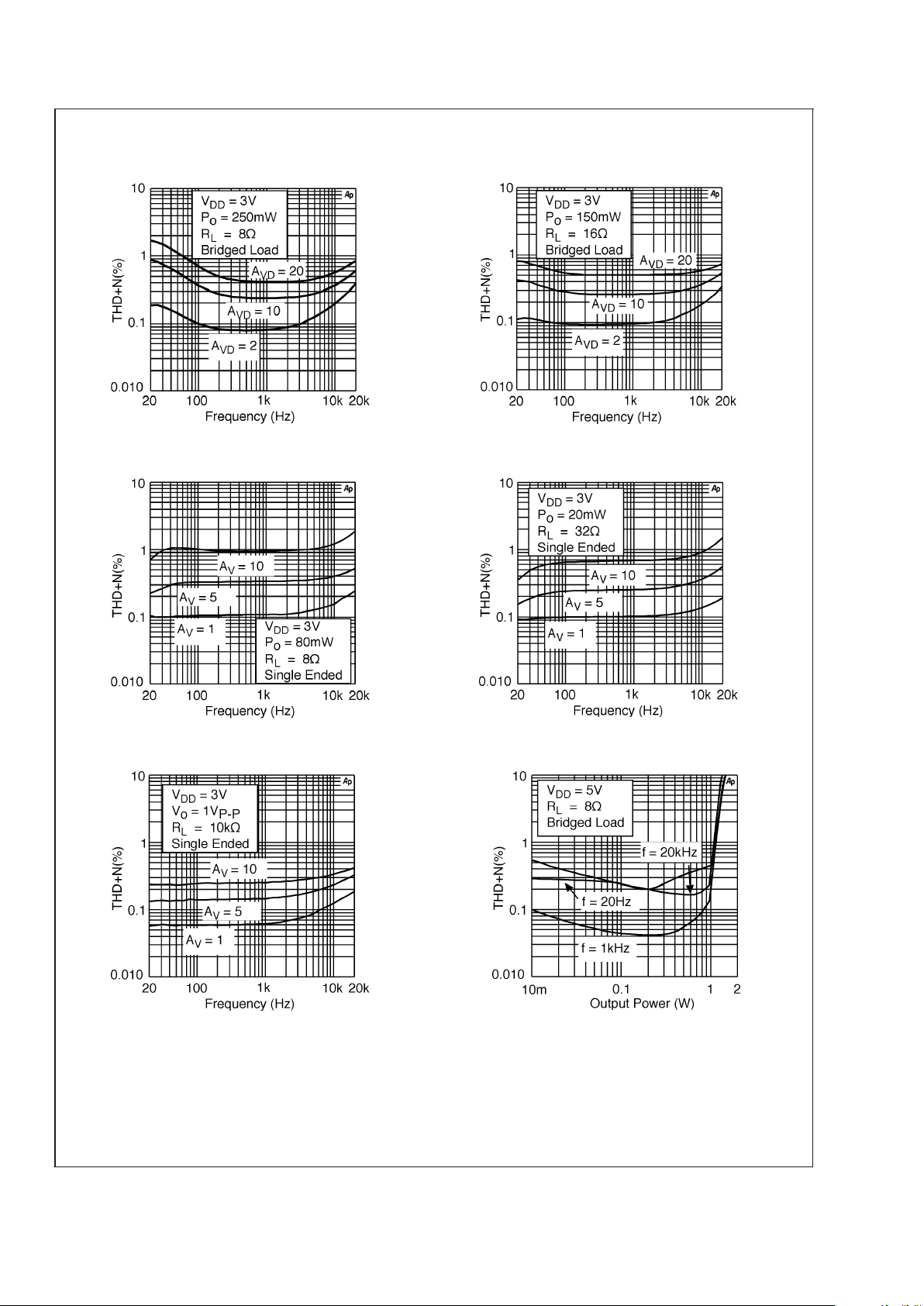
Non-MTE Specific Characteristics
THD+N vs Frequency THD+N vs Frequency
20013357
20013358
THD+N vs Frequency THD+N vs Frequency
20013314
20013315
THD+N vs Frequency THD+N vs Frequency
20013316
20013317
LM4838
www.national.com 8
Page 9
Non-MTE Specific Characteristics (Continued)
THD+N vs Frequency THD+N vs Frequency
20013318 20013319
THD+N vs Frequency THD+N vs Frequency
20013320
20013321
THD+N vs Frequency THD+N vs Output Power
20013322
20013324
LM4838
www.national.com9
Page 10
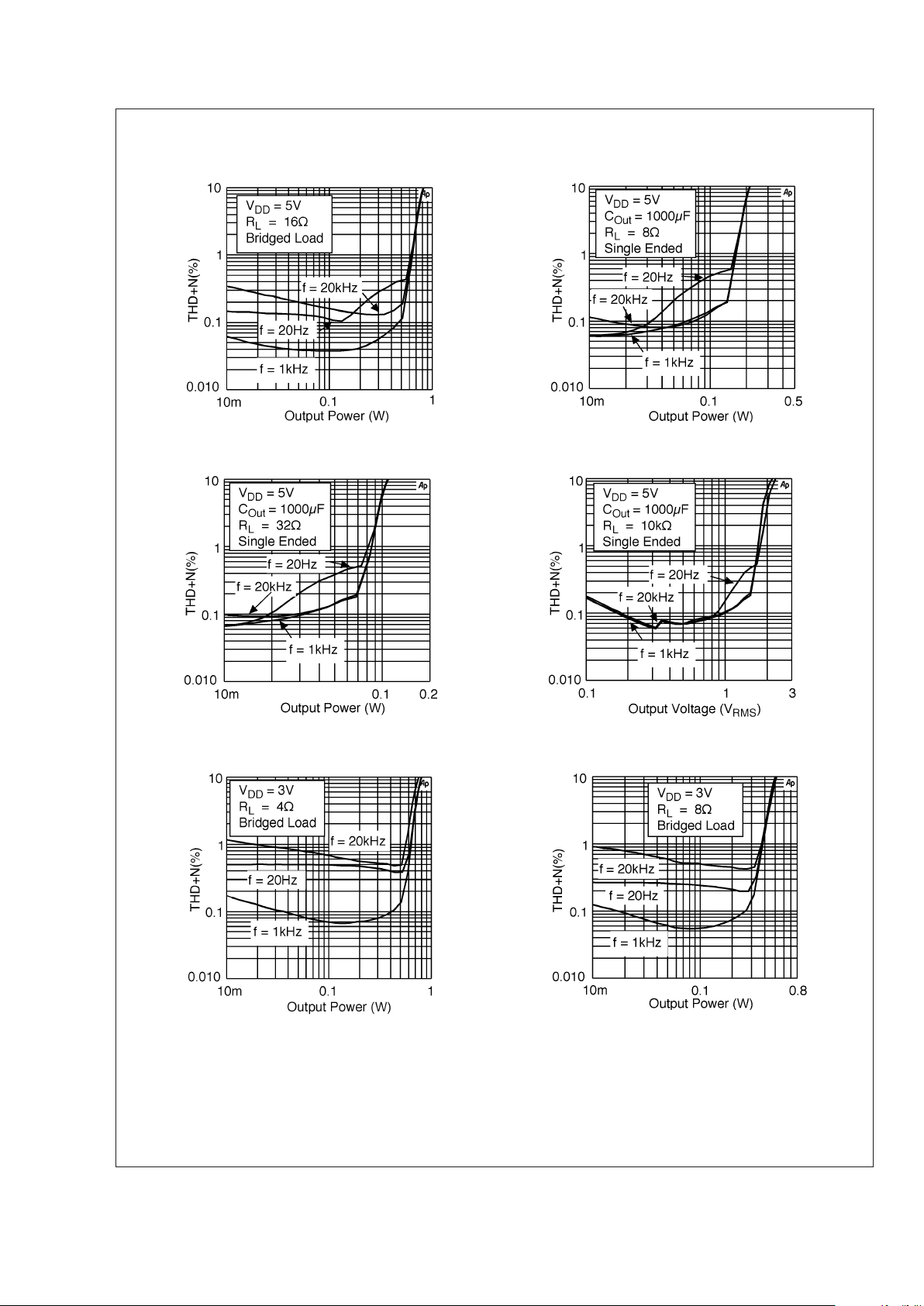
Non-MTE Specific Characteristics (Continued)
THD+N vs Output Power THD+N vs Output Power
20013325
20013326
THD+N vs Output Power THD+N vs Output Power
20013327
20013328
THD+N vs Output Power THD+N vs Output Power
20013329
20013330
LM4838
www.national.com 10
Page 11
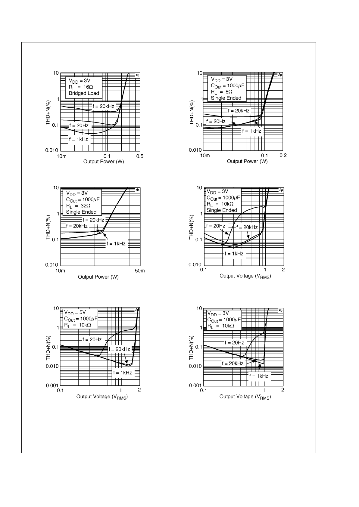
Non-MTE Specific Characteristics (Continued)
THD+N vs Output Power THD+N vs Output Power
20013331
20013332
THD+N vs Output Power THD+N vs Output Power
20013333
20013334
THD+N vs Output Voltage
Docking Station Pins
THD+N vs Output Voltage
Docking Station Pins
20013359
20013360
LM4838
www.national.com11
Page 12

Typical Performance Characteristics
Output Power vs
Load Resistance Dropout Voltage
20013362
20013353
Output Power vs
Load Resistance
Output Power vs
Load Resistance
20013306
20013307
Power Supply
Rejection Ratio
Output Power vs
Load Resistance
20013339
20013308
LM4838
www.national.com 12
Page 13

Typical Performance Characteristics (Continued)
Noise Floor Noise Floor
20013341
20013342
Volume Control
Characteristics
External Gain/
Bass Boost Characteristics
20013340
20013361
Power Dissipation vs
Output Power
Power Dissipation vs
Output Power
20013351 20013352
LM4838
www.national.com13
Page 14

Typical Performance Characteristics (Continued)
Power Derating Curve Crosstalk
20013363
20013349
Output Power
vs Supply voltage
Output Power
vs Supply Voltage
20013354 20013356
Supply Current
vs Supply Voltage
LM4838ITL (Note 19)
Power Derating Curve
20013309
20013394
Note 19: These curves show the thermal dissipation of the LM4838ITL at different ambient temperatures with a thermal plane of size shown on an outside PCB layer
using 1oz. copper.
LM4838
www.national.com 14
Page 15

Application Information
EXPOSED-DAP PACKAGE PCB MOUNTING
CONSIDERATIONS
The LM4838’s exposed-DAP (die attach paddle) packages
(MTE, LQ) provide a low thermal resistance between the die
and the PCB to which the part is mounted and soldered. This
allows rapid heat transfer from the die to the surrounding
PCB copper traces, ground plane and, finally, surrounding
air. The result is a low voltage audio power amplifier that
produces 2.1W at ≤ 1% THD with a 4Ω load. This high power
is achieved through careful consideration of necessary thermal design. Failing to optimize thermal design may compromise the LM4838’s high power performance and activate
unwanted, though necessary, thermal shutdown protection.
The MTE and LQ packages must have their exposed DAPs
soldered to a grounded copper pad on the PCB. The DAP’s
PCB copper pad is connected to a large grounded plane of
continuous unbroken copper. This plane forms a thermal
mass heat sink and radiation area. Place the heat sink area
on either outside plane in the case of a two-sided PCB, or on
an inner layer of a board with more than two layers. Connect
the DAP copper pad to the inner layer or backside copper
heat sink area with 32(4x8) (MTE) or 6(3x2) (LQ) vias. The
via diameter should be 0.012in–0.013in with a 1.27mm
pitch. Ensure efficient thermal conductivity by platingthrough and solder-filling the vias.
Best thermal performance is achieved with the largest practical copper heat sink area. If the heatsink and amplifier
share the same PCB layer, a nominal 2.5in
2
(min) area is
necessary for 5V operation with a 4Ω load. Heatsink areas
not placed on the same PCB layer as the LM4838 MTE and
LQ packages should be 5in
2
(min) for the same supply
voltage and load resistance. The last two area recommendations apply for 25˚C ambient temperature. Increase the
area to compensate for ambient temperatures above 25˚C.
In systems using cooling fans, the LM4838MTE can take
advantage of forced air cooling. With an air flow rate of 450
linear-feet per minute and a 2.5in
2
exposed copper or 5.0in
2
inner layer copper plane heatsink, the LM4838MTE can
continuously drive a 3Ω load to full power. The LM4838LQ
achieves the same output power level without forced air
cooling. In all circumstances and conditions, the junction
temperature must be held below 150˚C to prevent activating
the LM4838’s thermal shutdown protection. The LM4838’s
power de-rating curve in the Typical Performance Charac-
teristics shows the maximum power dissipation versus temperature. Example PCB layouts for the exposed-DAP
TSSOP and LQ packages are shown in the Demonstration
Board Layout section. Further detailed and specific information concerning PCB layout, fabrication, and mounting an
LQ (LLP) package is available in National Semiconductor’s
AN1187.
The micro SMD package (LM4838ITL) thermals work in a
similar way to the LQ and MTE packages in that a thermal
plane increases the heat transfer from the die. The thermal
plane can be any electrical potential but needs to be below
the package to aid in the spreading the heat from the die out
to surrounding PCB areas to reduce the thermal resistance
of the micro SMD package. The thermal plane is most effective when placed on the top or first internal PCB layers. The
traces connecting the bumps also contribute to spreading
heat away from the die. The same recommendations for the
size of the thermal plane as given above apply for the ITL
package, namely 2.5in
2
minimum for top layer thermal plane
and 5in
2
minimum for internal or bottom layers.
PCB LAYOUT AND SUPPLY REGULATION
CONSIDERATIONS FOR DRIVING 3Ω AND 4Ω LOADS
Power dissipated by a load is a function of the voltage swing
across the load and the load’s impedance. As load impedance decreases, load dissipation becomes increasingly dependent on the interconnect (PCB trace and wire) resistance
between the amplifier output pins and the load’s connections. Residual trace resistance causes a voltage drop,
which results in power dissipated in the trace and not in the
load as desired. For example, 0.1Ω trace resistance reduces
the output power dissipated by a 4Ω load from 2.1W to 2.0W.
This problem of decreased load dissipation is exacerbated
as load impedance decreases. Therefore, to maintain the
highest load dissipation and widest output voltage swing,
PCB traces that connect the output pins to a load must be as
wide as possible.
Poor power supply regulation adversely affects maximum
output power. A poorly regulated supply’s output voltage
decreases with increasing load current. Reduced supply
voltage causes decreased headroom, output signal clipping,
and reduced output power. Even with tightly regulated supplies, trace resistance creates the same effects as poor
supply regulation. Therefore, making the power supply
traces as wide as possible helps maintain full output voltage
swing.
BRIDGE CONFIGURATION EXPLANATION
As shown in Figure 2, the LM4838 output stage consists of
two pairs of operational amplifiers, forming a two-channel
(channel A and channel B) stereo amplifier. (Though the
following discusses channel A, it applies equally to channel
B.)
Figure 2 shows that the first amplifier’s negative (-) output
serves as the second amplifier’s input. This results in both
amplifiers producing signals identical in magnitude, but 180˚
out of phase. Taking advantage of this phase difference, a
load is placed between −OUTA and +OUTA and driven differentially (commonly referred to as “bridge mode”). This
results in a differential gain of
A
VD
=2*(Rf/Ri) (1)
Bridge mode amplifiers are different from single-ended amplifiers that drive loads connected between a single amplifier’s output and ground. For a given supply voltage, bridge
mode has a distinct advantage over the single-ended configuration: its differential output doubles the voltage
swing across the load. This produces four times the output
power when compared to a single-ended amplifier under the
same conditions. This increase in attainable output power
assumes that the amplifier is not current limited or that the
output signal is not clipped. To ensure minimum output signal clipping when choosing an amplifier’s closed-loop gain,
refer to the Audio Power Amplifier Design section.
Another advantage of the differential bridge output is no net
DC voltage across the load. This is accomplished by biasing
channel A’s and channel B’s outputs at half-supply. This
eliminates the coupling capacitor that single supply, singleended amplifiers require. Eliminating an output coupling capacitor in a single-ended configuration forces a single-supply
amplifier’s half-supply bias voltage across the load. This
increases internal IC power dissipation and may permanently damage loads such as speakers.
LM4838
www.national.com15
Page 16

Application Information (Continued)
POWER DISSIPATION
Power dissipation is a major concern when designing a
successful single-ended or bridged amplifier. Equation (2)
states the maximum power dissipation point for a singleended amplifier operating at a given supply voltage and
driving a specified output load.
P
DMAX
=(VDD)
2
/(2π2RL) Single-Ended (2)
However, a direct consequence of the increased power delivered to the load by a bridge amplifier is higher internal
power dissipation for the same conditions.
The LM4838 has two operational amplifiers per channel. The
maximum internal power dissipation per channel operating in
the bridge mode is four times that of a single-ended amplifier. From Equation (3), assuming a 5V power supply and a
4Ω load, the maximum single channel power dissipation is
1.27W or 2.54W for stereo operation.
P
DMAX
=4*(VDD)2/(2π2RL) Bridge Mode (3)
The LM4838’s power dissipation is twice that given by Equation (2) or Equation (3) when operating in the single-ended
mode or bridge mode, respectively. Twice the maximum
power dissipation point given by Equation (3) must not exceed the power dissipation given by Equation (4):
P
DMAX
'=(T
JMAX−TA
)/θ
JA
(4)
The LM4838’s T
JMAX
= 150˚C. In the LQ package soldered
to a DAP pad that expands to a copper area of 5in
2
on a
PCB, the LM4838’s θ
JA
is 20˚C/W. In the MTE package
soldered to a DAP pad that expands to a copper area of 2in
2
on a PCB, the LM4838MTE’s θJAis 41˚C/W. For the
LM4838MT package, θ
JA
= 80˚C/W. At any given ambient
temperature T
A
, use Equation (4) to find the maximum internal power dissipation supported by the IC packaging. Rearranging Equation (4) and substituting P
DMAX
for P
DMAX
' results in Equation (5). This equation gives the maximum
ambient temperature that still allows maximum stereo power
dissipation without violating the LM4838’s maximum junction
temperature.
T
A=TJMAX
– 2*P
DMAXθJA
(5)
For a typical application with a 5V power supply and an 4Ω
load, the maximum ambient temperature that allows maximum stereo power dissipation without exceeding the maximum junction temperature is approximately 99˚C for the LQ
package and 45˚C for the MTE package.
T
JMAX=PDMAXθJA+TA
(6)
Equation (6) gives the maximum junction temperature
T
JMAX
. If the result violates the LM4838’s 150˚C T
JMAX
,
reduce the maximum junction temperature by reducing the
power supply voltage or increasing the load resistance. Further allowance should be made for increased ambient temperatures.
The above examples assume that a device is a surface
mount part operating around the maximum power dissipation
point. Since internal power dissipation is a function of output
power, higher ambient temperatures are allowed as output
power or duty cycle decreases.
If the result of Equation (2) is greater than that of Equation
(3), then decrease the supply voltage, increase the load
impedance, or reduce the ambient temperature. If these
measures are insufficient, a heat sink can be added to
reduce θ
JA
. The heat sink can be created using additional
copper area around the package, with connections to the
ground pin(s), supply pin and amplifier output pins. External,
solder attached SMT heatsinks such as the Thermalloy
7106D can also improve power dissipation. When adding a
heat sink, the θ
JA
is the sum of θJC, θCS, and θSA.(θJCis the
junction-to-case thermal impedance, θ
CS
is the case-to-sink
thermal impedance, and θ
SA
is the sink-to-ambient thermal
impedance.) Refer to the Typical Performance Character-
istics curves for power dissipation information at lower output power levels.
POWER SUPPLY BYPASSING
As with any power amplifier, proper supply bypassing is
critical for low noise performance and high power supply
rejection. Applications that employ a 5V regulator typically
use a 10 µF in parallel with a 0.1 µF filter capacitor to
stabilize the regulator’s output, reduce noise on the supply
line, and improve the supply’s transient response. However,
their presence does not eliminate the need for a local 1.0µF
tantalum bypass capacitance connected between the
LM4838’s supply pins and ground. Do not substitute a ceramic capacitor for the tantalum. Doing so may cause oscillation. Keep the length of leads and traces that connect
capacitors between the LM4838’s power supply pin and
ground as short as possible. Connecting a 1µF capacitor,
C
B
, between the BYPASS pin and ground improves the
internal bias voltage’s stability and the amplifier’s PSRR. The
PSRR improvements increase as the BYPASS pin capacitor
value increases. Too large a capacitor, however, increases
turn-on time and can compromise the amplifier’s click and
pop performance. The selection of bypass capacitor values,
especially C
B
, depends on desired PSRR requirements,
click and pop performance (as explained in the following
section, Selecting Proper External Components), system
cost, and size constraints.
SELECTING PROPER EXTERNAL COMPONENTS
Optimizing the LM4838’s performance requires properly selecting external components. Though the LM4838 operates
well when using external components with wide tolerances,
best performance is achieved by optimizing component values.
The LM4838 is unity-gain stable, giving a designer maximum
design flexibility. The gain should be set to no more than a
given application requires. This allows the amplifier to
achieve minimum THD+N and maximum signal-to-noise ratio. These parameters are compromised as the closed-loop
gain increases. However, low gain circuits demand input
signals with greater voltage swings to achieve maximum
output power. Fortunately, many signal sources such as
audio CODECs have outputs of 1V
RMS
(2.83V
P-P
). Please
refer to the Audio Power Amplifier Design section for more
information on selecting the proper gain.
LM4838
www.national.com 16
Page 17

Application Information (Continued)
INPUT CAPACITOR VALUE SELECTION
Amplifying the lowest audio frequencies requires a high
value input coupling capacitor (0.33µF in Figure 2), but high
value capacitors can be expensive and may compromise
space efficiency in portable designs. In many cases, however, the speakers used in portable systems, whether internal or external, have little ability to reproduce signals below
150 Hz. Applications using speakers with this limited frequency response reap little improvement by using a large
input capacitor.
Besides effecting system cost and size, the input coupling
capacitor has an affect on the LM4838’s click and pop performance. When the supply voltage is first applied, a transient (pop) is created as the charge on the input capacitor
changes from zero to a quiescent state. The magnitude of
the pop is directly proportional to the input capacitor’s size.
Higher value capacitors need more time to reach a quiescent
DC voltage (usually V
DD
/2) when charged with a fixed current. The amplifier’s output charges the input capacitor
through the feedback resistor, R
f
. Thus, pops can be minimized by selecting an input capacitor value that is no higher
than necessary to meet the desired −6dB frequency.
As shown in Figure 2, the input resistor (R
IR,RIL
= 20k) ( and
the input capacitor (C
IR,CIL
= 0.33µF) produce a −6dB high
pass filter cutoff frequency that is found using Equation (7).
(7)
As an example when using a speaker with a low frequency
limit of 150Hz, the input coupling capacitor, using Equation
(7), is 0.053µF. The 0.33µF input coupling capacitor shown
in Figure 2 allows the LM4838 to drive a high efficiency, full
range speaker whose response extends below 30Hz.
OPTIMIZING CLICK AND POP REDUCTION
PERFORMANCE
The LM4838 contains circuitry that minimizes turn-on and
shutdown transients or “clicks and pops”. For this discussion, turn-on refers to either applying the power supply voltage or when the shutdown mode is deactivated. While the
power supply is ramping to its final value, the LM4838’s
internal amplifiers are configured as unity gain buffers. An
internal current source changes the voltage of the BYPASS
pin in a controlled, linear manner. Ideally, the input and
outputs track the voltage applied to the BYPASS pin. The
gain of the internal amplifiers remains unity until the voltage
on the BYPASS pin reaches 1/2 V
DD
. As soon as the voltage
on the BYPASS pin is stable, the device becomes fully
operational. Although the BYPASS pin current cannot be
modified, changing the size of C
B
alters the device’s turn-on
time and the magnitude of “clicks and pops”. Increasing the
value of C
B
reduces the magnitude of turn-on pops. How-
ever, this presents a tradeoff: as the size of C
B
increases, the
turn-on time increases. There is a linear relationship between the size of C
B
and the turn-on time. Here are some
typical turn-on times for various values of C
B
:
C
B
T
ON
0.01µF 2ms
C
B
T
ON
0.1µF 20ms
0.22µF 44ms
0.47µF 94ms
1.0µF 200ms
DOCKING STATION INTERFACE
Applications such as notebook computers can take advantage of a docking station to connect to external devices such
as monitors or audio/visual equipment that sends or receives
line level signals. The LM4838 has two outputs, Right Dock
and Left Dock, which connect to outputs of the internal input
amplifiers that drive the volume control inputs. These input
amplifiers can drive loads of
>
1kΩ (such as powered speakers) with a rail-to-rail signal. Since the output signal present
on the RIGHT DOCK and LEFT DOCK pins is biased to
V
DD
/2, coupling capacitors should be connected in series
with the load when using these outputs. Typical values for
the output coupling capacitors are 0.33µF to 1.0µF. If polarized coupling capacitors are used, connect their "+" terminals to the respective output pin, see Figure 2.
Since the DOCK outputs precede the internal volume control, the signal amplitude will be equal to the input signal’s
magnitude and cannot be adjusted. However, the input amplifier’s closed-loop gain can be adjusted using external
resistors. These 20k resistors (R
FR,RFL
) are shown in Fig-
ure 2 and they set each input amplifier’s gain to -1. Use
Equation 7 to determine the input and feedback resistor
values for a desired gain.
-A
VR=RFR/RIR
and - AVL=RFL/R
IL
(8)
Adjusting the input amplifier’s gain sets the minimum gain for
that channel. Although the single ended output of the Bridge
Output Amplifiers can be used to drive line level outputs, it is
recommended that theR&LDock Outputs simpler signal
path be used for better performance.
BEEP DETECT FUNCTION
Computers and notebooks produce a system “beep“ signal
that drives a small speaker. The speaker’s auditory output
signifies that the system requires user attention or input. To
accommodate this system alert signal, the LM4838’s beep
input pin is a mono input that accepts the beep signal.
Internal level detection circuitry at this input monitors the
beep signal’s magnitude. When a signal level greater than
V
DD
/2 is detected on the BEEP IN pin, the bridge output
amplifiers are enabled. The beep signal is amplified and
applied to the load connected to the output amplifiers. A valid
beep signal will be applied to the load even when MUTE is
active. Use the input resistors connected between the BEEP
IN pin and the stereo input pins to accommodate different
beep signal amplitudes. These resistors (R
BEEP
) are shown
as 200kΩ devices in Figure 2. Use higher value resistors to
reduce the gain applied to the beep signal. The resistors
must be used to pass the beep signal to the stereo inputs.
The BEEP IN pin is used only to detect the beep signal’s
magnitude: it does not pass the signal to the output amplifiers. The LM4838’s shutdown mode must be deactivated
before a system alert signal is applied to BEEP IN pin.
LM4838
www.national.com17
Page 18

Application Information (Continued)
MICRO-POWER SHUTDOWN
The voltage applied to the SHUTDOWN pin controls the
LM4838’s shutdown function. Activate micro-power shutdown by applying V
DD
to the SHUTDOWN pin. When active,
the LM4838’s micro-power shutdown feature turns off the
amplifier’s bias circuitry, reducing the supply current. The
logic threshold is typically V
DD
/2. The low 0.7 µA typical
shutdown current is achieved by applying a voltage that is as
near as V
DD
as possible to the SHUTDOWN pin. A voltage
that is less than V
DD
may increase the shutdown current.
There are a few ways to control the micro-power shutdown.
These include using a single-pole, single-throw switch, a
microprocessor, or a microcontroller. When using a switch,
connect an external 10kΩ pull-up resistor between the
SHUTDOWN pin and V
DD
. Connect the switch between the
SHUTDOWN pin and ground. Select normal amplifier operation by closing the switch. Opening the switch connects the
SHUTDOWN pin to V
DD
through the pull-up resistor, activating micro-power shutdown. The switch and resistor guarantee that the SHUTDOWN pin will not float. This prevents
unwanted state changes. In a system with a microprocessor
or a microcontroller, use a digital output to apply the control
voltage to the SHUTDOWN pin. Driving the SHUTDOWN pin
with active circuitry eliminates the need for a pull up resistor.
MODE FUNCTION
The LM4838’s MODE function has 2 states controlled by the
voltage applied to the MODE pin. Mode 0, selected by
applying 0V to the MODE pin, forces the LM4838 to effectively function as a "line-out," unity-gain amplifier. Mode 1,
which uses the internal DC controlled volume control is
selected by applying V
DD
to the MODE pin. This mode sets
the amplifier’s gain according to the DC voltage applied to
the DC VOL CONTROL pin. Unanticipated gain behavior can
be prevented by connecting the MODE pin to V
DD
or ground.
Note: Do not let the mode pin float.
MUTE FUNCTION
The LM4838 mutes the amplifier and DOCK outputs when
V
DD
is applied to the MUTE pin. Even while muted, the
LM4838 will amplify a system alert (beep) signal whose
magnitude satisfies the BEEP DETECT circuitry. Applying
0V to the MUTE pin returns the LM4838 to normal, unmuted
operation. Prevent unanticipated mute behavior by connecting the MUTE pin to V
DD
or ground. Do not let the mute pain
float.
HP SENSE FUNCTION ( Head Phone In )
Applying a voltage between 4V and V
DD
to the LM4838’s
HP-IN headphone control pin turns off the amps that drive
the Left out "+" and Right out "+" pins. This action mutes a
bridged-connected load. Quiescent current consumption is
reduced when the IC is in this single-ended mode.
Figure 3 shows the implementation of the LM4838’s headphone control function. With no headphones connected to
the headphone jack, the R1-R2 voltage divider sets the
voltage applied to the HP SENSE pin at approximately
50mV. This 50mV puts the LM4838 into bridged mode operation. The output coupling capacitor blocks the amplifier’s
half supply DC voltage, protecting the headphones.
The HP-IN threshold is set at 4V. While the LM4838 operates
in bridged mode, the DC potential across the load is essentially 0V. Therefore, even in an ideal situation, the output
swing cannot cause a false single-ended trigger. Connecting
headphones to the headphone jack disconnects the headphone jack contact pin from R2 and allows R1 to pull the HP
Sense pin up to V
DD
through R4. This enables the headphone function, turns off both of the "+" output amplifiers,
and mutes the bridged speaker. The remaining single-ended
amplifiers then drive the headphones, whose impedance is
in parallel with resistors R2 and R3. These resistors have
negligible effect on the LM4838’s output drive capability
since the typical impedance of headphones is 32Ω.
Figure 3 also shows the suggested headphone jack electrical connections. The jack is designed to mate with a threewire plug. The plug’s tip and ring should each carry one of
the two stereo output signals, whereas the sleeve should
carry the ground return. A headphone jack with one control
pin contact is sufficient to drive the HP-IN pin when connecting headphones.
A microprocessor or a switch can replace the headphone
jack contact pin. When a microprocessor or switch applies a
voltage greater than 4V to the HP-IN pin, a bridge-connected
speaker is muted and the single ended output amplifiers 1A
and 2A will drive a pair of headphones.
20013304
FIGURE 3. Headphone Sensing Circuit
LM4838
www.national.com 18
Page 19

Application Information (Continued)
GAIN SELECT FUNCTION (Bass Boost)
The LM4838 features selectable gain, using either internal or
external feedback resistors. Either set of feedback resistors
set the gain of the output amplifiers. The voltage applied to
the GAIN SELECT pin controls which gain is selected. Applying V
DD
to the GAIN SELECT pin selects the external gain
mode. Applying 0V to the GAIN SELECT pin selects the
internally set unity gain.
In some cases a designer may want to improve the low
frequency response of the bridged amplifier or incorporate a
bass boost feature. This bass boost can be useful in systems
where speakers are housed in small enclosures. A resistor,
R
LFE
, and a capacitor, C
LFE
, in parallel, can be placed in
series with the feedback resistor of the bridged amplifier as
seen in Figure 4.
At low, frequencies C
LFE
is a virtual open circuit and at high
frequencies, its nearly zero ohm impedance shorts R
LFE
.
The result is increased bridge-amplifier gain at low frequencies. The combination of R
LFE
and C
LFE
form a -6dB corner
frequency at
f
C
= 1/(2πR
LFECLFE
) (9)
The bridged-amplifier low frequency differential gain is:
A
VD
= 2(RF+R
LFE
)/R
i
(10)
Using the component values shown in Figure 1 (R
F
= 20kΩ,
R
LFE
= 20kΩ, and C
LFE
= 0.068µF), a first-order, -6dB pole is
created at 120Hz. Assuming R
i
= 20kΩ, the low frequency
differential gain is 4. The input (C
i
) and output (CO) capacitor
values must be selected for a low frequency response that
covers the range of frequencies affected by the desired
bass-boost operation.
DC VOLUME CONTROL
The LM4838 has an internal stereo volume control whose
setting is a function of the DC voltage applied to the DC VOL
CONTROL pin.
The LM4838 volume control consists of 31 steps that are
individually selected by a variable DC voltage level on the
volume control pin. The range of the steps, controlled by the
DC voltage, are from 0dB - 78dB. Each gain step corresponds to a specific input voltage range, as shown in table 2.
To minimize the effect of noise on the volume control pin,
which can affect the selected gain level, hysteresis has been
implemented. The amount of hysteresis corresponds to half
of the step width, as shown in Volume Control Characterization Graph (DS200133-40).
For highest accuracy, the voltage shown in the ’recommended voltage’ column of the table is used to select a
desired gain. This recommended voltage is exactly halfway
between the two nearest transitions to the next highest or
next lowest gain levels.
The gain levels are 1dB/step from 0dB to -6dB, 2dB/step
from -6dB to -36dB, 3dB/step from -36dB to -47dB, 4dB/step
from -47db to -51dB, 5dB/step from -51dB to -66dB, and
12dB to the last step at -78dB.
20013311
FIGURE 4. Low Frequency Enhancement
LM4838
www.national.com19
Page 20

Application Information (Continued)
VOLUME CONTROL TABLE ( Table 2 )
Gain
(dB)
Voltage Range (% of Vdd) Voltage Range (Vdd = 5) Voltage Range (Vdd = 3)
Low High Recommended Low High Recommended Low High Recommended
0 77.5% 100.00% 100.000% 3.875 5.000 5.000 2.325 3.000 3.000
-1 75.0% 78.5% 76.875% 3.750 3.938 3.844 2.250 2.363 2.306
-2 72.5% 76.25% 74.375% 3.625 3.813 3.719 2.175 2.288 2.231
-3 70.0% 73.75% 71.875% 3.500 3.688 3.594 2.100 2.213 2.156
-4 67.5% 71.25% 69.375% 3.375 3.563 3.469 2.025 2.138 2.081
-5 65.0% 68.75% 66.875% 3.250 3.438 3.344 1.950 2.063 2.006
-6 62.5% 66.25% 64.375% 3.125 3.313 3.219 1.875 1.988 1.931
-8 60.0% 63.75% 61.875% 3.000 3.188 3.094 1.800 1.913 1.856
-10 57.5% 61.25% 59.375% 2.875 3.063 2.969 1.725 1.838 1.781
-12 55.0% 58.75% 56.875% 2.750 2.938 2.844 1.650 1.763 1.706
-14 52.5% 56.25% 54.375% 2.625 2.813 2.719 1.575 1.688 1.631
-16 50.0% 53.75% 51.875% 2.500 2.688 2.594 1.500 1.613 1.556
-18 47.5% 51.25% 49.375% 2.375 2.563 2.469 1.425 1.538 1.481
-20 45.0% 48.75% 46.875% 2.250 2.438 2.344 1.350 1.463 1.406
-22 42.5% 46.25% 44.375% 2.125 2.313 2.219 1.275 1.388 1.331
-24 40.0% 43.75% 41.875% 2.000 2.188 2.094 1.200 1.313 1.256
-26 37.5% 41.25% 39.375% 1.875 2.063 1.969 1.125 1.238 1.181
-28 35.0% 38.75% 36.875% 1.750 1.938 1.844 1.050 1.163 1.106
-30 32.5% 36.25% 34.375% 1.625 1.813 1.719 0.975 1.088 1.031
-32 30.0% 33.75% 31.875% 1.500 1.688 1.594 0.900 1.013 0.956
-34 27.5% 31.25% 29.375% 1.375 1.563 1.469 0.825 0.937 0.881
-36 25.0% 28.75% 26.875% 1.250 1.438 1.344 0.750 0.862 0.806
-39 22.5% 26.25% 24.375% 1.125 1.313 1.219 0.675 0.787 0.731
-42 20.0% 23.75% 21.875% 1.000 1.188 1.094 0.600 0.712 0.656
-45 17.5% 21.25% 19.375% 0.875 1.063 0.969 0.525 0.637 0.581
-47 15.0% 18.75% 16.875% 0.750 0.937 0.844 0.450 0.562 0.506
-51 12.5% 16.25% 14.375% 0.625 0.812 0.719 0.375 0.487 0.431
-56 10.0% 13.75% 11.875% 0.500 0.687 0.594 0.300 0.412 0.356
-61 7.5% 11.25% 9.375% 0.375 0.562 0.469 0.225 0.337 0.281
-66 5.0% 8.75% 6.875% 0.250 0.437 0.344 0.150 0.262 0.206
-78 0.0% 6.25% 0.000% 0.000 0.312 0.000 0.000 0.187 0.000
LM4838
www.national.com 20
Page 21

Application Information (Continued)
AUDIO POWER AMPLIFIER DESIGN
Audio Amplifier Design: Driving 1W into an 8Ω Load
The following are the desired operational parameters:
Power Output: 1 W
RMS
Load Impedance: 8Ω
Input Level: 1 V
RMS
Input Impedance: 20 kΩ
Bandwidth: 100 Hz−20 kHz
±
0.25 dB
The design begins by specifying the minimum supply voltage
necessary to obtain the specified output power. One way to
find the minimum supply voltage is to use the Output Power
vs Supply Voltage curve in the Typical Performance Char-
acteristics section. Another way, using Equation (10), is to
calculate the peak output voltage necessary to achieve the
desired output power for a given load impedance. To account for the amplifier’s dropout voltage, two additional voltages, based on the Dropout Voltage vs Supply Voltage in the
Typical Performance Characteristics curves, must be
added to the result obtained by Equation (10). The result is
Equation (11).
(11)
VDD≥ (V
OUTPEAK
+(V
OD
TOP
+V
OD
BOT
)) (12)
The Output Power vs Supply Voltage graph for an 8Ω load
indicates a minimum supply voltage of 4.6V. This is easily
met by the commonly used 5V supply voltage. The additional
voltage creates the benefit of headroom, allowing the
LM4838 to produce peak output power in excess of 1W
without clipping or other audible distortion. The choice of
supply voltage must also not create a situation that violates
of maximum power dissipation as explained above in the
Power Dissipation section.
After satisfying the LM4838’s power dissipation requirements, the minimum differential gain needed to achieve 1W
dissipation in an 8Ω load is found using Equation (12).
(13)
Thus, a minimum overall gain of 2.83 allows the LM4838’s to
reach full output swing and maintain low noise and THD+N
performance.
The last step in this design example is setting the amplifier’s
−6dB frequency bandwidth. To achieve the desired
±
0.25dB
pass band magnitude variation limit, the low frequency response must extend to at least one-fifth the lower bandwidth
limit and the high frequency response must extend to at least
five times the upper bandwidth limit. The gain variation for
both response limits is 0.17dB, well within the
±
0.25dB
desired limit. The results are an
f
L
= 100Hz/5 = 20Hz (14)
and an
f
H
= 20kHz x 5 = 100kHz (15)
As mentioned in the Selecting Proper External Compo-
nents section, R
i
(Right & Left) and Ci(Right & Left) create
a highpass filter that sets the amplifier’s lower bandpass
frequency limit. Find the input coupling capacitor’s value
using Equation (14).
C
i
≥ 1/(2πRifL) (16)
The result is
1/(2π
*
20kΩ*20Hz) = 0.397µF (17)
Use a 0.39µF capacitor, the closest standard value.
The product of the desired high frequency cutoff (100kHz in
this example) and the differential gain A
VD
, determines the
upper passband response limit. With A
VD
= 3 and fH=
100kHz, the closed-loop gain bandwidth product (GBWP) is
300kHz. This is less than the LM4838’s 3.5MHz GBWP. With
this margin, the amplifier can be used in designs that require
more differential gain while avoiding performance,restricting
bandwidth limitations.
Recommended Printed Circuit
Board Layout
The following figures show the recommended PC board
layouts that are optimized for the different package options
of the LM4838 and associated external components. This
circuit is designed for use with an external 5V supply and 4Ω
speakers.
This circuit board is easy to use. Apply 5V and ground to the
board’s V
DD
and GND pads, respectively. Connect 4Ω
speakers between the board’s −OUTA and +OUTA and
OUTB and +OUTB pads.
LM4838
www.national.com21
Page 22

Recommended Printed Circuit Board Layout (Continued)
20013377
FIGURE 5. Recommended LQ PC Board Layout:
Component-Side Silkscreen
20013378
FIGURE 6. Recommended LQ PC Board Layout:
Component-Side Layout
LM4838
www.national.com 22
Page 23

Recommended Printed Circuit Board Layout (Continued)
20013379
FIGURE 7. Recommended LQ PC Board Layout:
Upper Inner-Layer Layout
20013380
FIGURE 8. Recommended LQ PC Board Layout:
Lower Inner-Layer Layout
LM4838
www.national.com23
Page 24

Recommended Printed Circuit Board Layout (Continued)
20013381
FIGURE 9. Recommended LQ PC Board Layout:
Bottom-Side Layout
LM4838
www.national.com 24
Page 25

Analog Audio LM4838 LLP28 Eval Board
Assembly Part Number: 980011368-100
Revision: A1
Bill of Material
Item Part Number Part Description Qty Ref Designator Remark
1 551011368-001 LM4838 Eval Board PCB etch 001 1
10 482911368-001 LM4838 28L LLP 1 U4
20 151911368-001 Cer Cap 0.068µF 50V 10% 1206 2 CBS1, CBS2
25 152911368-001 Tant Cap 0.1µF 10V 10% Size = A 3216 3 CS1, CS2, CV
26 152911368-002 Tant Cap 0.33µF 10V 10% Size = A 3216 3 Cin1, Cin2, Cin3
27 152911368-003 Tant Cap 1µF 16V 10% Size = A 3216 3 CB, C01, C02
28 152911368-004 Tant Cap 10µF 10V 10% Size = C 6032 1 CS3
29 152911368-005 Tant Cap 220µF 16V 10% Size = D 7343 2 Cout1, Cout2
30 472911368-001 Res 1.5K Ohm 1/8W 1% 1206 2 RL1, RL2
31 472911368-002 Res 20k Ohm 1/8W 1% 1206 10 Rin1, Rin2, RF1, RF2
Rl1, Rl2, RBS1, RBS2
Rdock1, Rdock2
32 472911368-003 Res 100k Ohm 1/8W 1% 1206 2 RS, RPU
33 472911368-004 Res 200k Ohm 1/16W 1% 0603 2 Rbeep1, Rbeep2
40 131911368-001 Stereo Headphone Jack W/ Switch 1 U2 Mouser # 161-3500
41 131911368-002 Slide Switch 4 Mode, Mute, Gain, SD Mouser # 10SP003
42 131911368-003 Potentiometer 1 U1 Mouser # 317-290-100K
43 131911368-004 RCA Jack 3 RightIn, BeepIn, LeftIn Mouser # 16PJ097
44 131911368-005 Banana Jack, Black 3 GND, Right Out-, Left Out- Mouser # ME164-6219
45 131911368-006 Banana Jack, Red 3 Vdd, Right Out+, Left Out+ Mouser # ME164-6218
LM4838
www.national.com25
Page 26

LM4838 MT & MTE Demo Board Artwork
20013382
Top Layer SilkScreen
20013383
Top Layer TSSOP
LM4838
www.national.com 26
Page 27

LM4838 MT & MTE Demo Board Artwork (Continued)
20013385
Inner Layer (2) LM4838MT/MTE
20013386
Inner Layer (3) LM4838MT/MTE
LM4838
www.national.com27
Page 28

LM4838 MT & MTE Demo Board Artwork (Continued)
20013384
Bottom Layer TSSOP
Analog Audio LM4838 TSSOP Eval Board
Assembly Part Number: 980011373-100
Revision: A
Bill of Material
Item Part Number Part Description Qty Ref Designator Remark
1 551011373-001 LM4838 Eval Board PCB
etch 001
1
10 482911373-001 LM4838 TSSOP 1
20 151911368-001 Cer Cap 0.068µF 50V
10% 1206
2 CBS
25 152911368-001 Tant Cap 0.1µF 10V 10%
Size = A 3216
3 CS, CS, CV
26 152911368-002 Tant Cap 0.33µF 10V
10% Size = A 3216
3 CIN
27 152911368-003 Tant Cap 1µF 16V 10%
Size = A 3216
3 CB, CO1, CO2
28 152911368-004 Tant Cap 10µF 10V 10%
Size = C 6032
1 CS1
29 152911368-005 Tant Cap 220µF 16V 10%
Size = D 7343
2 CoutL, R
30 472911368-001 Res 1.5K Ohm 1/8W 1%
1206
2RL
31 472911368-002 Res 20K Ohm 1/8W 1%
1206
10 RIN(4), RF(2),
RDOCK(2),
RBS(2)
32 472911368-003 Res 100K Ohm 1/8W 1%
1206
2 RPU, RS
33 472911368-004 Res 200K Ohm 1/16W
1% 0603
2 RBEEP
LM4838
www.national.com 28
Page 29

Analog Audio LM4838 TSSOP Eval Board
Assembly Part Number: 980011373-100
Revision: A
Bill of Material (Continued)
Item Part Number Part Description Qty Ref Designator Remark
40 131911368-001 Stereo Headphone Jack
W/ Switch
1 Mouser #
161-3500
41 131911368-002 Slide Switch 4 mute, mode, Gain,SDMouser #
10SP003
42 131911368-003 Potentiometer 1 Volume Control Mouser #
317-2090-100K
43 131911368-004 RCA Jack 3 Right-In, Beep-In,
Left-In
Mouser #
16PJ097
44 131911368-005 Banana Jack, Black 3 Mouser #
ME164-6219
45 131911368-006 Banana Jack, Red 3 Mouser #
ME164-6218
LM4838
www.national.com29
Page 30

LM4838 ITL Demo Board Artworks
20013392
FIGURE 10. LM4838 micro SMD Silk Screen
20013389
FIGURE 11. LM4838 micro SMD Top Layer
LM4838
www.national.com 30
Page 31

LM4838 ITL Demo Board Artworks (Continued)
20013390
FIGURE 12. LM4838 micro SMD Upper Inner Layer
20013391
FIGURE 13. LM4838 micro SMD Lower Inner Layer
LM4838
www.national.com31
Page 32

LM4838 ITL Demo Board Artworks (Continued)
20013393
FIGURE 14. LM4838 micro SMD Bottom Layer
LM4838
www.national.com 32
Page 33

Analog Audio LM4838 TLA36 Board
Bill of Material
Part Description µΩ Qty Reference Designator
LM4838 TLA36 Evaluation Board PCB 1 P/N: 551011755 - 002 rev A
LM4838ITL 1 U1
Ceramic Capacitor 0.068µF 50V 10%
Size = 1206
2 CBS1, CBS2
Tantalum Capacitor 0.1µF 10V 10%
Size = 1206
3 CS1, CS2, CV
Tantalum Capacitor 0.33µF 10V 10%
Size = 1206
3 CIN1, CIN2, CIN3
Tantalum Capacitor 1.0µF 16V 10%
Size = 1210
4 CS3, CB, CO1, CO2
Tantalum Capacitor 220µF 16V 10%
Size = 7343
2 COUT1, COUT2
Resistor 1.5kΩ 1/10W 1%
Size = 0805
2 RL1, RL2
Resistor 20kΩ 1/10W 1%
Size = 0805
10 RIN1, RIN2, RF1, RF2, Rl1, Rl2, RBS1,
RBS2, RDOCK1, RDOCK2
Resistor 100kΩ 1/10W 1%
Size = 0805
2 RS, RPU
Resistor 120kΩ 1/10W 1%
Size = 0805
2 RBEEP1, RBEEP2
Resistor 1MΩ 1/10W 1%
Size = 0805
1RV
Jumper Header Vertical Mount
0.100” spacing
1 J1 (Docking RT LF)
RCA Jack PCB mount 3 J2 (LeftIn), J3 (Beep In), J4 (Right In)
Banana Jack, Black 3 J5B (GND), J6A (Right Out -), J7A (Left Out
-)
Banana Jack, Red 3 J5A (V
DD
), J6B (Right Out +), J7B (Left Out
+)
Stereo Headphone Jack W/Switch 1 J8
Single Turn Potentiometer 100kΩ 20% 1 J9
Jumper Header Vertical Mount
0.100” spacing 3x4
1 Mute, SD, Gain, Mode
Jumper Header Vertical Mount
0.100” spacing 1x3
1DCIN
LM4838
www.national.com33
Page 34

Physical Dimensions inches (millimeters) unless otherwise noted
LLP Package
Order Number LM4838LQ
NS Package Number LQA028AA For Exposed-DAP LLP
LM4838
www.national.com 34
Page 35

Physical Dimensions inches (millimeters) unless otherwise noted (Continued)
TSSOP Package
Order Number LM4838MT
NS Package Number MTC28 for TSSOP
Exposed-DAP TSSOP Package
Order Number LM4838MTE
NS Package Number MXA28A for Exposed-DAP TSSOP
LM4838
www.national.com35
Page 36

Physical Dimensions inches (millimeters) unless otherwise noted (Continued)
36-Bump micro SMD
Order Number LM4838ITL, LM4838ITLX
NS Package Number TLA36AAA
X
1
= 3.000±0.03 X2= 3.000±0.03 X3= 0.600±0.075
LIFE SUPPORT POLICY
NATIONAL’S PRODUCTS ARE NOT AUTHORIZED FOR USE AS CRITICAL COMPONENTS IN LIFE SUPPORT
DEVICES OR SYSTEMS WITHOUT THE EXPRESS WRITTEN APPROVAL OF THE PRESIDENT AND GENERAL
COUNSEL OF NATIONAL SEMICONDUCTOR CORPORATION. As used herein:
1. Life support devices or systems are devices or
systems which, (a) are intended for surgical implant
into the body, or (b) support or sustain life, and
whose failure to perform when properly used in
accordance with instructions for use provided in the
labeling, can be reasonably expected to result in a
significant injury to the user.
2. A critical component is any component of a life
support device or system whose failure to perform
can be reasonably expected to cause the failure of
the life support device or system, or to affect its
safety or effectiveness.
National Semiconductor
Americas Customer
Support Center
Email: new.feedback@nsc.com
Tel: 1-800-272-9959
National Semiconductor
Europe Customer Support Center
Fax: +49 (0) 180-530 85 86
Email: europe.support@nsc.com
Deutsch Tel: +49 (0) 69 9508 6208
English Tel: +44 (0) 870 24 0 2171
Français Tel: +33 (0) 1 41 91 8790
National Semiconductor
Asia Pacific Customer
Support Center
Fax: 65-6250 4466
Email: ap.support@nsc.com
Tel: 65-6254 4466
National Semiconductor
Japan Customer Support Center
Fax: 81-3-5639-7507
Email: nsj.crc@jksmtp.nsc.com
Tel: 81-3-5639-7560
www.national.com
LM4838 Stereo 2W Audio Power Amplifiers with DC Volume Control and Selectable Gain
National does not assume any responsibility for use of any circuitry described, no circuit patent licenses are implied and National reserves the right at any time without notice to change said circuitry and specifications.
 Loading...