

Page 1
LM4831
Multimedia Computer Audio Chip
General Description
The LM4831 is a monolithic integrated circuit that provides a
stereo three input mixer,twostereoinputanalogmultiplexer,
a stereo line out and a dual 1W bridged audio power amplifier. In addition, a low noise microphone preamp is included
on-chip.
The LM4831 is ideal for multimedia computers since it incorporates an input mixer, analog multiplexer, and configurable
stereo audio power amplifier, as well as a microphone
preamp stage. This combination allows for all of the analog
audio processing to be enclosed in a 44-pin TQFP package.
The LM4831 features an externally controlled, low-power
consumption shutdown mode, as well as both headphone
and docking station modes.Totemporarilyoverridetheshutdown mode and allow audio signals to be amplified, the
LM4831 provides four “beep” pins.
Key Specifications
n THD+N at 1W into 8Ω 0.6%(typ)
n Microphone Input Referred Noise 10µV (typ)
n Supply Current - Bridged Mode 16mA (typ)
n Shutdown Current 2µA (typ)
Features
n Stereo 1W audio power amplifier
n “Click and pop” suppression circuitry
n Stereo three input mixer
n Shutdown mode
n Multiple operating modes— bridged, single-ended and
docking station modes
n Internal mux for switching in/out external filter
n Beep circuitry for “wake-up” while in shutdown
n 44 Pin TQFP Packaging
Applications
n Portable and Desktop Computers
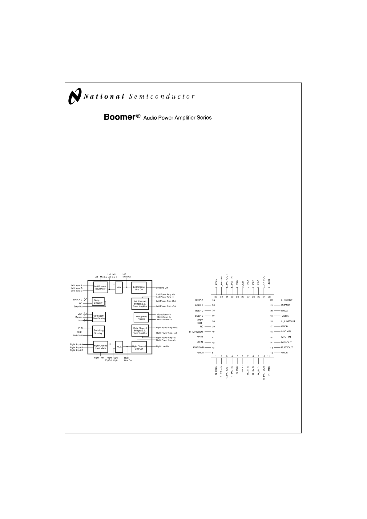
Block Diagram Connection Diagram
Boomer®is a registered trademark of National Semiconductor Corporation.
TRI-STATE
®
is a registered trademark of National Semiconductor Corporation.
DS100057-1
FIGURE 1. LM4831 Block Diagram
DS100057-3
Top View
Order Number LM4831VF
See NS Package Number VEJ44A
November 1998
LM4831 Multimedia Computer Audio Chip
© 1998 National Semiconductor Corporation DS100057 www.national.com
Page 2
Absolute Maximum Ratings (Note 2)
If Military/Aerospace specified devices are required,
please contact the National Semiconductor Sales Office/
Distributors for availability and specifications.
Supply Voltage 6.0V
Storage Temperature −65˚C to 150˚C
Input Voltage −0.3V to V
DD
+0.3V
Power Dissipation (Note 3) Internally limited
ESD Susceptibility (Note 4) 2500V
ESD Susceptibility (Note 5) 200V
Junction Temperature 150˚C
Soldering Information
Small Outline Package
Vapor Phase (60 sec.) 215˚C
Infrared (15 sec.) 220˚C
See AN-450 “Surface Mounting and their Effects on
Product Reliability” for other methods of soldering
surface mount devices.
Thermal Resistance
θ
JC
(typ) 15˚C/W
θ
JA
(typ) 62˚C/W
Operating Ratings
Temperature Range −40˚C to 85˚C
Supply Voltage 2.7 ≤ V
DD
≤ 5.5V
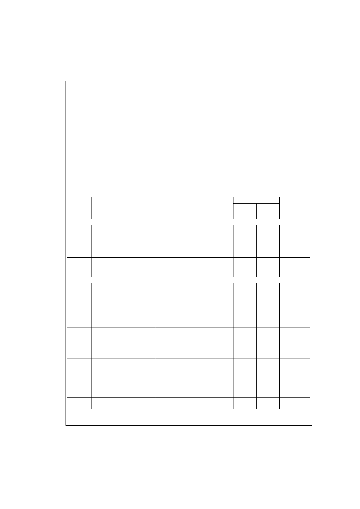
Electrical Characteristics
(Notes 1, 2) The following specifications apply for VDD= 5V, RL=8Ωandf=1kHz, unless otherwise specified. Distortion
measurements represent the full audio chain from Input A of each channel to their respective output. Limits apply for
T
A
= 25˚C.
Symbol Parameter Conditions
LM4831
Units
(Limits)
Typical
(Note
6)
Limit
(Note
7)
General Characteristics For Entire IC
V
DD
Supply Voltage 2.7 V (min)
5.5 V (max)
I
DD
Quiescent Power Supply
Current
Bridged Mode, IO= 0 mA 16 50 mA (max)
Single-Ended Mode, I
O
= 0 mA 10.5 mA
Docking Station Mode, I
O
=0mA 7 mA
I
SD
Shutdown Current V
PIN-43
= 5V, V
PIN-41=VPIN-42
= 0V 2 50 µA (max)
V
DD/2
Half Supply Bypass Voltage VIN= 0V, V
Pin-43
= 0V 2.45 2.4 V (min)
2.6 V (max)
Power Amplifiers
P
O
Output Power - Bridged
Mode
RL=8Ω,THD = 1
%
1.1 1 W (min)
R
L
=4Ω,THD=1
%
1.5 W
Output Power Single-Ended Mode
R
L
=8Ω,THD=1
%
300 mW
R
L
=4Ω,THD=1
%
550 mW
THD Total Harmonic Distortion Bridged Mode, P
O
= 1W, RL=8Ω 0.5 2.0
%
(Max)
Single-Ended Mode, P
O
= 225mW,
R
L
=8Ω
0.15
%
V
OS
Output Offset Voltage VIN= 0V 5 50 mV (Max)
E
Noise
Input Referred Noise A-Weighted Filter, VIN= 0V,
R
L
=8Ω
Bridged Output 45 100 µV (max)
Single-Ended Output 35 100 µV (max)
PSRR Power Supply Rejection
Ratio
f = 1kHz, C
B
= 0.5µF, RL=8Ω
Bridged Output 47 dB
Single-Ended Output 45 dB
X
TALK
Channel to Channel
Crosstalk
f = 1kHz, PO= 1W, RL=8Ω
Right to Left −82 dB
Left to Right −73 dB
I
TS
TRI-STATE®Current-Single
Ended Mode
V
PIN-41
= 4.0V, L_PA+OUT =
R_PA+OUT = V
DD
or GND
80 100 µA (max)
www.national.com 2
Page 3
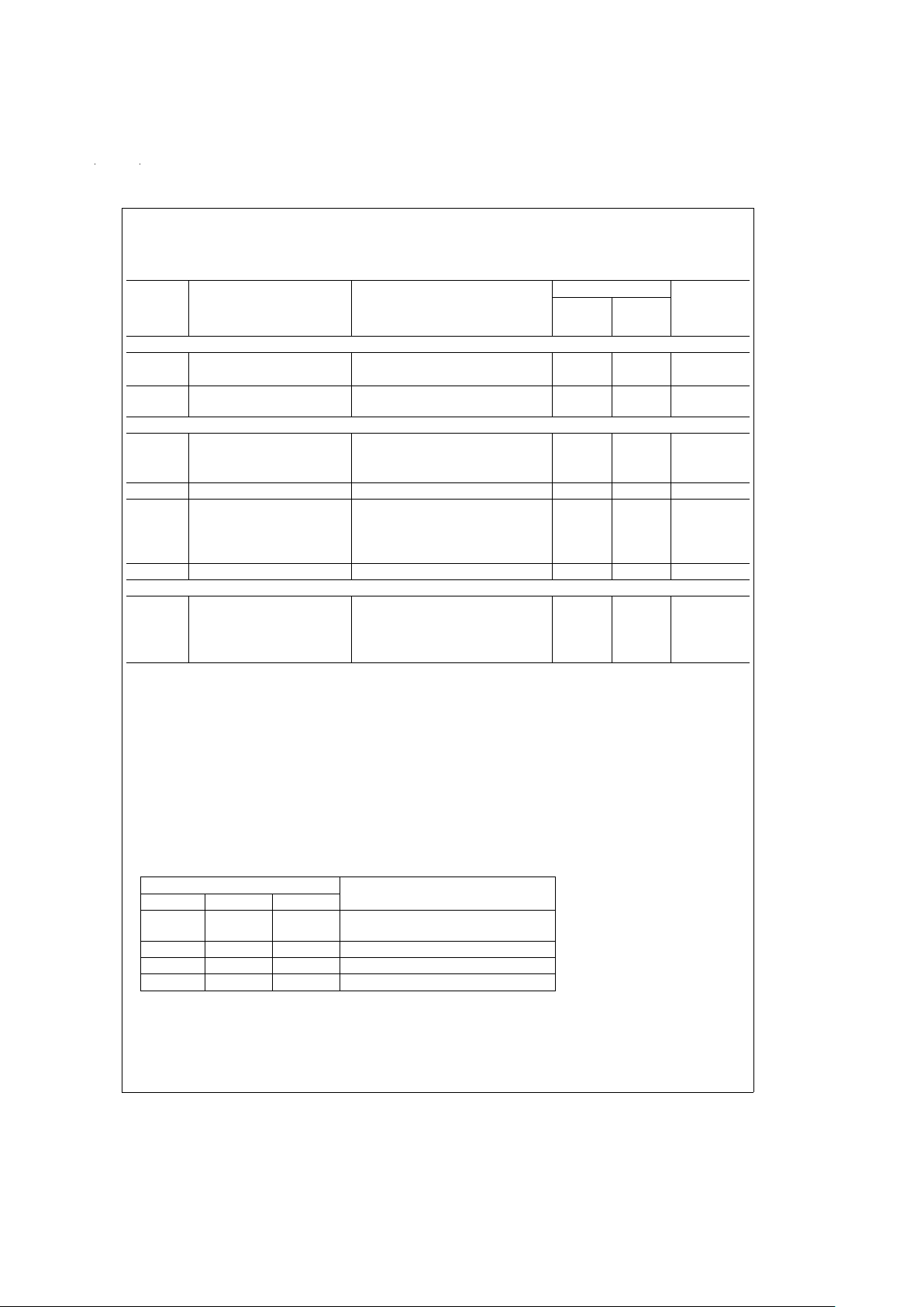
Electrical Characteristics (Continued)
(Notes 1, 2) The following specifications apply for VDD= 5V, RL=8Ωandf=1kHz, unless otherwise specified. Distortion
measurements represent the full audio chain from Input A of each channel to their respective output. Limits apply for
T
A
= 25˚C.
Symbol Parameter Conditions
LM4831
Units
(Limits)
Typical
(Note
6)
Limit
(Note
7)
Microphone Amplifier
THD Total Harmonic Distortion R
L
=10kΩ,VIN=1V
RMS
0.15
%
E
Noise
Input Referred Noise A-−weighted Filter 10 18 µV (max)
X
TALK
Crosstalk Amplifier Bridged Output, f = 1kHz,
P
O
= 1W, R
L-mic
= 20kΩ
95 dB
Other Audio Characteristics
THD Total Harmonic Distortion R
L
=20kΩ,VIN=1V
RMS
Line Out 0.15 0.5
%
(max)
Equalizer Out 0.01
%
E
Noise
Input Referred Noise A-weighted filter, Line Out 20 100 µV (max)
A
V
Channel Path Gain Line Out
±
0.1
±
0.7 dB (max)
Equalizer Out
±
0.1
±
0.6 dB (max)
MUX Out −0.25 −0.85,
+0.3
dB
E
T
Stereo Tracking Error Line Out
±
0.1
±
0.5 dB (max)
Digital Inputs and Outputs
V
IL
Input Low Voltage 1.0 V (max)
V
IH
Input High Voltage 4.0 V (min)
V
OL
Output Low Voltage 0.5 V (max)
V
OH
Output High Voltage 3.5 V (min)
Note 1: All voltages are measured with respect to the ground pins, 12, 17, 20, and 44, unless otherwise specified.
Note 2:
Absolute Maximum Ratings
indicate limits beyond which damage to the device may occur.
Operating Ratings
indicate conditions for which the device is func-
tional, but do not guarantee specific performance limits.
Electrical Characteristics
state DC and AC electrical specifications under particular test conditions which guarantee specific performance limits. This assumes that the device is within the Operating Ratings. Specifications are not guaranteed for parameters where no limit is
given, however, the typical value is a good indication of device performance.
Note 3: The maximum power dissipation must be derated at elevated temperatures and is dictated by T
JMAX
, θJA, and the ambient temperature TA. The maximum
allowable power dissipation is P
DMAX
=(T
JMAX−TA
)/θJA. For the LM4831, T
JMAX
= 150˚C, and the typical junction-to-ambient thermal resistance, when board
mounted, is 62˚C/W assuming the VEF44A package.
Note 4: Human body model, 100 pF discharged through a 1.5 kΩ resistor.
Note 5: Machine Model, 220 pF–240 pF discharged through all pins.
Note 6: Typicals are measured at 25˚C and represent the parametric norm.
Note 7: Limits are guaranteed to National’s AOQL (Average Outgoing Quality Level).
Digital Inputs Pin Truth Table
Pin Name LM4831 State
PWRDWN HPIN DSIN
0 0 0 Bridged Outputs Active
Equalizer In/Out Active
0 0 1 Line-Outs Active
0 1 X(Note 8) Single-Ended Outputs Active
1 X X Shutdown
Note 8: “X” means that the state of that pin does not matter in that particular input combination.
www.national.com3
Page 4
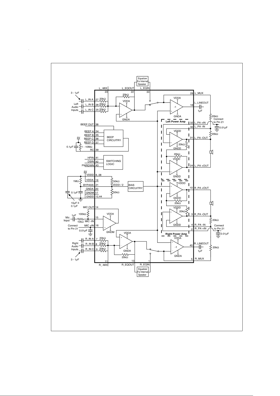
Typical Application
DS100057-2
FIGURE 3. Typical Application Circuit
www.national.com 4
Page 5

Pin Descriptions
VDDA This is the analog power supply pin
which powers all internal circuitry, with
the exceptions of the output amplifiers
and the digital logic in the Beep and
Switching circuit sections. This pin
should be connected to the same
supply voltage as the two VDDD pins
(typically 5V), but have a separate
ground return path to the supply
ground to minimize interaction with the
high current amplifier returns and
digital switching noise. In addition, this
pin should be bypassed with a 0.01
µF–0.1 µF capacitor.
VDDD These pins are the “digital” and high
current power supply pins which
power the stereo bridged output
amplifier and the digital logic in the
Beep and Switching circuit sections.
These pins should be connected to
the same supply voltage as the VDDA
pin (typically 5V), but have a separate
return path to the supply to avoid
interferring with low level signals. In
addition, this pin should be bypassed
with a 0.01 µF–0.1 µF capacitor. At
the power supply connection, a bulk
storage capacitor of at least 10 µF will
reduce the instantaneous current
demanded from the power supply.
GNDA,
GNDD,
GNDM
These are the power supply ground
pins. GNDA is the ground pin for the
low current analog circuitry. The two
GNDD pins are for the digital logic
and bridged output amplifiers. GNDM
is the ground for the microphone
amplifier. Make sure that the high
current GNDD paths are not returned
through the low current GNDM or
GNDA paths. These four ground pins
should be star-grounded at a stable,
low-impedance, noise-free system
ground.
BYPASS This voltage at this pin is nominally
1/2 VDDD and is created by an
internal 50 kΩ resistor divider. This
node should be bypassed with a
capacitor value from 0.1 µF-1.0 µF.
Increasing the capacitor value will
increase the ramp time of the
amplifiers, thereby improving turn-on
pop performance. 0.1µF is typical for
the bypass capacitor. In addition, a 1
MΩ resistor from the bypass pin to the
positive supply is shown in
Figure 3
.
This resistor guarantees that the
LM4831 will turn-on if the device is
powered up with both the PWRDWN
and DS-IN pins high. If the the
LM4831 will never enter that state,
then the 1MΩ resistor can be
removed.
HP-IN This pin places the output power
amplifier in “headphone” mode. If
HP-IN is low, the amplifier is in
bridged mode and the 2:1 mux passes
the input on the EQ_IN pin. If HP-IN is
high, the amplifier is in single-ended
mode and the 2:1 mux passes the
output of the mixing stage.
Single-ended mode places the
non-inverting amplifier in the output
amplifiers into a high impedance state.
HP-IN also has priority over the DS-IN
pin, so if HP-IN and DS-IN are both
high, the device is in single-ended
mode and the stereo line out amplifier
is in a high-impedance state.
DS-IN This pin is used to put the LM4831
into “docking-station” mode and
control the line out drivers and the
state of the internal 2:1 analog
multiplexer. If DS-IN is high, the
stereo line out amplifier is on and the
stereo bridged amplifier is in a high
impedance state. Asserting the DS-IN
pin also changes the 2:1 analog
multiplexer output from the stereo
signal on the L_EQIN and R_EQIN
pins to the internal path from the
stereo input mixer.
www.national.com5
Page 6

Pin Descriptions (Continued)
PWRDWN This pin is used to power down the
entire IC (except BEEP Circuitry).
Placing a logic high on the PWRDWN
pin will place the LM4831 in a low
supply current state. To minimize the
shutdown-mode supply current, the
PWRDWN pin should be pulled up to
the voltage on the LM4831 power
supply pins. The PWRDWN pin is
overridden if an edge change occurs
on any of the BEEP A–D inputs.
L_INA,
L_INB,
L_INC
These pins are the left channel inputs.
Typical input impedance on each input
is 20 kΩ.
R_INA,
R_INB,
R_INC
These pins are the right channel
inputs. Typical input impedance on
each input is 20 kΩ.
L_MIX,
R_MIX
These pins are the inverting input
nodes of the input mixer for the left
and right channel, respectively.
L_EQOUT,
R_EQOUT
These are the outputs of the input
mixer for the left and right channel,
respectively. This output is generally
fed to an external filter to equalize the
response of internal computer
speakers and then back into the EQIN
pins.
L_EQIN,
R_EQIN
These pins are one of the two inputs
to the 2:1 analog multiplexer and are
used to feed in externally filtered
versions of the EQOUT signals. The
2:1 multiplexer selects the signal on
L_EQIN and R_EQIN if the HP_IN
and DS_IN pins are both low.
L_MUX,
R_MUX
These are the stereo outputs of the
2:1 analog multiplexer. The output of
the 2:1 multiplexer is decided by the
state of the HP-IN and DS-IN pins. If
both HP-IN and DS-IN are low, the 2:1
mux selects the analog input on the
EQIN pins. If either HP-IN or DS-IN is
high, the 2:1 mux selects the internal
analog path. See .
L_LINEOUT,
R_LINEOUT
These are the line outputs for the left
and right channel, respectively.
Although these outputs are capable of
driving a wide range of resistive loads,
they are typically used to drive an
impedance of at least 10 kΩ. These
outputs are only enabled when the
DS-IN pin is high, otherwise, they are
in a high-impedance state.
L_PA+IN,
R_PA+IN
These pins are the positive inputs of
the output audio power amplifiers.
Since the power amplifier is typically
configured as an inverting amplifier,
these pins should be connected to the
BYPASS pin to properly bias the
output power amplifiers. Further, these
pins should be individually bypassed
with a capacitor of 0.01 µF–0.1 µF.
L_PA−IN,
R_PA−IN
These pins are the inverting inputs for
the output audio power amplifier for
the left and right channel, respectively.
L_PA−OUT,
R_PA−OUT
These pins are the inverted power
amp outputs for the left and right
channel, respectively. In bridged mode
(DS-IN = HP_IN = PWRDWN = low),
each output drives one terminal of a
direct coupled bridged speaker. In
single-ended (headphone) mode,
(HP_IN = high, PWRDWN = low,
DS-IN = N/A) these outputs drive a
capacitively coupled stereo
headphone. In docking station mode
(DS-IN = high, HP_IN = PWRDWN =
low), these outputs are disabled.
L_PA+OUT,
R_PA+OUT
These pins are the non-inverted power
amp outputs for the left and right
channel, respectively. In bridged mode
(DS-IN = HP_IN = PWRDWN = low),
each output drives one terminal of a
direct coupled bridged speaker. In
single-ended (headphone) mode
(HP_IN = high, PWRDWN = low,
DS-IN = N/A), these outputs are in a
high impedance state, effectively
muting the bridged loudspeaker. In
docking station mode (DS-IN = high,
HP_IN = PWRDWN = low), these
outputs are disabled.
www.national.com 6
Page 7

Pin Descriptions (Continued)
MIC+IN This pin is the positive input of the
microphone amplifier. The microphone
amplifier is typically configured as an
inverting amplifier, so this pin should
be connected to the BYPASS pin to
properly bias the amplifier. Further,
this pin should be individually
bypassed with a capacitor of
0.01µF–0.1 µF.
MIC−IN This pin is the inverting input for the
microphone amplifier. Because the
microphone amplifier is typically used
as an inverting amplifier, this pin
should be capacitor coupled to the
input signal.
MIC OUT This pin is the microphone amplifier
output. If this pin is to be connected to
any chips other than the LM4831, it
should be capacitor coupled to the
load.
BEEP A,
BEEP B,
BEEP C,
BEEP D
These four pins are used to “wake up”
the LM4831 for a specified amount of
time (dictated by the parallel resistor
and capacitor connected to the RC
pin). If the device is in shutdown and
an edge appears at any of the four
BEEP pins, then the device will
power-up, pass the sound, and then
power-down again.
BEEP OUT This pin outputs the result of an
exclusive-or of the four BEEP inputs.
BEEP OUT connects back to the
Audio Codec as a status pin.
RC This pin is connected to an external
resistor-capacitor network which sets
the on-time for a beep request.
Typically, a 0.1µF capacitor is
paralleled with a 1–10MΩ resistor.
Typical Performance Characteristic
Supply Current vs
Supply Voltage
DS100057-31
Power Derating Curve
DS100057-23
THD+N vs Frequency
DS100057-5
THD+N vs Frequency
DS100057-4
THD+N vs Frequency
DS100057-29
www.national.com7
Page 8

Typical Performance Characteristic (Continued)
THD+N vs Frequency
DS100057-17
THD+N vs Output Power
DS100057-11
THD+N vs Output Power
DS100057-6
THD+N vs Output Power
DS100057-14
THD+N vs Output Power
DS100057-15
THD+N vs Output Power
DS100057-16
Power Amplifier Noise Floor
DS100057-28
Power Amplifer
Crosstalk, Bridged
DS100057-13
Power Amplifer
Crosstalk, Bridged
DS100057-12
Power Amplifier
Crosstalk to Mic
DS100057-21
Power Amplifier PSRR
DS100057-30
www.national.com 8
Page 9

Typical Performance Characteristic (Continued)
Power Dissipation,
Bridged
DS100057-25
Power Dissipation,
Single-Ended
DS100057-26
Ouput Power vs Supply Voltage
Bridged
DS100057-24
Ouput Power vs Supply Voltage
Single-Ended
DS100057-27
Output Power vs Load
DS100057-22
Microphone
THD+N vs Frequency
DS100057-19
Microphone
THD+N vs Output Level
DS100057-18
Microphone
Noise Floor
DS100057-20
Line Out
THD+N vs Frequency
DS100057-9
Line Out
Noise Floor
DS100057-10
Equalizer Output
THD+N vs Frequency
DS100057-7
www.national.com9
Page 10

Typical Performance Characteristic (Continued)
Application Information
GROUNDING
Certain grounding techniques should be followed when laying out the LM4831 circuit.
Figure 4
shows how to setup the
grounds for the LM4831. The half-supply bypass ground
should be tied with the input source grounds and brought
back to the power supply ground separately from the output
load grounds. in with the input grounds. Bringing the output
load grounds back to the supply separately will keep large
signal currents from interfering with the stable input ground
references.
LAYOUT
As stated in the Grounding section, placement of ground return lines is critical for maintaining the highest level of system performance. It is not only important to route the correct
ground return lines together, but also important to be aware
of where those ground return lines are routed relative to
each other. The output load ground returns should be physically located as far as reasonably possible from low signal
level lines and their ground return lines. The layout of the microphone amplifier signal lines is critical, since these lines
generally work at very low signal levels.
SUPPLY BYPASSING
As with all op amps and power op amps, the LM4831 requires the power supplies to be bypassed to reduce distortion and avoid oscillation. To avoid high frequency instabilities, a 0.1µF metallized-film or ceramic capacitor should be
used to bypass each supply pin as near to the chip as possible. For low frequency considerations, a 10µF or greater
tantalum or electrolytic capacitor should be paralleled with
the high frequency bypass capacitor.
If power supply bypass capacitors are not sufficiently large,
the current in the power supply leads, which is a rectified version of the output current, may be fed back into internal circuitry. This internal feedback signal can cause high frequency distortion and oscillation.
If power supply lines to the chip are long, larger bypass capacitors could be required. Long power supply leads have inductance and resistance associated with them, which could
prevent peak low frequency current demands from being
met. The extra bypass capacitance will reduce the peak current requirements from the power supply lines.
Under certain conditions, the LM4831 may refuse to come
out of shutdown. A 1MΩ resistor connected from the power
supply to the bypass pin, as shown in the Typical Applica-
tion section circuit,
Figure 3
, will guarantee startup.
CLICK & POP CIRCUITRY AND THE BYPASS
CAPACITOR
The LM4831 contains circuitry to minimize turn-on transients. In this case, turn-on refers to either power supply
turn-on or the device coming out of shutdown mode. During
turn-on, an internal current source charges the bypass capacitor on the bypass pin. Both the inputs and outputs track
the voltage at the bypass pin. As soon as the bypass node is
stable at 1/2 V
DD
, the amplifier will become fully operational.
Although the bypass pin current source cannot be modified,
the size of the bypass capacitor, Cb, can be changed to alter
the device turn-on time and the amount of “click and pop”.
The relationship between the size of Cb and the turn-on time
is linear. By increasing Cb, the amount of turn-on pop can be
reduced. However, the trade-off for using a larger bypass capacitor is an increase in the turn-on time for the device. Re-
Equalizer Output
Noise Floor
DS100057-8
DS100057-99
FIGURE 4. Grounding Strategy for LM4831
www.national.com 10
Page 11

Application Information (Continued)
ducing Cb will decrease turn-on time and increase “click and
pop”. If Cb is too small, the LM4831 can develop a
low-frequency oscillation (“motorboat”) when used at high
gains.
In order to eliminate “click and pop”, all coupling capacitors
must be discharged before turn-on. Rapid on/off switching of
the device or shutdown function may cause the “click and
pop” circuitry to not operate fully, resulting in increased “click
and pop” noise. For single-ended (headphone) circuitry, the
output coupling cap, C
o
, is of particular concern. In shutdown, this capacitor is discharged through an internal 20kΩ
resistor. Depending on the size of C
o
, the discharging time
constant can be quite large. To reduce the time constant, an
external 1kΩ-5kΩ resistor can be placed in parallel with the
internal 20kΩ resistor. The tradeoff for using this resistor is
an increase in quiescent current and an increase in turn-off
“click and pop”.
Changing the bypass capacitor size also affects the amount
of time that the beep circuitry turns on the LM4831. Increasing the bypass capacitor size increases the turn-on time,
which reduces the amount of time that the LM4831 is fully on
for during the RC-timed beep period.
The bypass capacitor also helps determine the power supply
rejection ratio. The smaller the bypass capacitor, the more
the power supply ripples couple onto the half supply and
then to all circuitry which uses the half supply for biasing.
COUPLING CAPACITORS
Since the LM4831 is a single supply circuit, all audio signals
(excepting the bridged outputs) must be capacitor coupled to
the chip to remove the 2.5V
DC
bias. All audio inputs have a
20kΩ input impedance, so the AC-coupling capacitor will create a high-pass filter with f
-3dB
= 1/(2π*20kΩ*Cin). For a
−3dB point at 20Hz, C
in
should be 0.39µF
Single-ended and line-out loads need to be AC-coupled back
to the LM4831 amplifiers. This high-pass filter is comprised
of the output load and the coupling capacitor, where the filter
cutoff is at f
-3dB
= 1/(2π*R
load*Cout
). If R
L
=
8Ω, then for a
−3dB point at 20Hz, C
out
should be 1000µF.
EQUALIZER INPUT/OUTPUT
In some systems, the internal speakers require filtering to
improve their frequency response. The LM4831 provides the
system designer with external access to the signal using the
equalizer output and equalizer inputpins. When the DS_IN
and HP_IN pins are low (ie. the system is not in the docking
station and no headphone are plugged in), an internal mux
routes the audio signal to the equalizer output pin. After the
signal is filtered, it is returned to the LM4831 audio path
through the equalizer inputpin.
The input impedance to the equalizer input pin is 20kΩ.Ifthe
external filter’s bias voltage is not derived from the half supply pin on the LM4831,AC-coupling capacitors must be used
on the equalizer input and output pins. If no equalization is
required, the equalizer out pin can be connected directly to
the equalizer in pin without any coupling capacitors.
LINE OUT
The line out pins are designed for use with a docking station
system. When the computer is plugged into the docking station, the DS_IN pin should be forced high, thereby turning off
the power amplifier outputs and turning on the line out amplifiers. All audio amplification and filtering is then done by the
docking station. The line out pins must be AC-coupled to the
docking station audio inputs.
POWER AMPLIFIERS
The power amplifiers in the LM4831 are designed to drive
8Ω or 32Ω loads at 1W (continuous) or 250mW(continuous),
respectively, with 1%THD+N. If the power amplifiers are
used to drive single-ended loads, such as headphones, the
amplifier inverting outputs should be AC-coupled to the output load. When the LM4831 is in headphone (single-ended)
mode, the amplifier non-inverting inputs are in a highimpedance state.
In low gain applications (A
V
<
5), the LM4831 may require a
small feedback capacitance to prevent oscillation. Typically,
5-10pF will prevent oscillation.
MICROPHONE AMPLIFIER
The microphone amplifier is an uncommitted op-amp which
is intended to amplify low-level signals. The microphone inputs are very high impedance (R
in
>
1MΩ) and can be directly connected to microphone networks. The microphone
amplifier has enough output capability to drive a 1kΩ load.
All microphone inputs and outputs must be AC-coupled.
As shown in
Figure 1
, the microphone amplifier is typically
configured as an inverting amplifier. The positive terminal is
connected to the half-supply bypass pin to properly bias the
amplifier output to interface with the other inputs on the
LM4831. The microphone input pin is connected to the inverting node of a CMOS op amp, so the input impedance is
very high (
>
10MΩ)
BEEP CIRCUITRY
The beep circuitry is designed to allow a “sleeping” system to
temporarily power-up the LM4831 and output an audio alert
(“beep”). This feature might be used in a computer which is
“sleeping”, but needs to notify the user that the computer
batteries are low or that the user has new e-mail.
The beep circuitry is activated by any edge which occurs on
the BEEP A-D pins. With a resistor, R
beep
, and a capacitor,
C
beep
, in parallel at the RC pin of the LM4831, the LM4831
will be activated for R
beepCbeep
seconds. Typical values for
R
beep
and R
beep
are 1-10ΩM and 0.1µF.
The BEEP OUT pin is designed to signal other audio circuitry
that the LM4831 is powering up. Generally a CODEC will receive this signal and begin sending audio information to the
LM4831. Logically, the BEEP OUT signal is the result of an
XOR of the BEEP A-D pins.
www.national.com11
Page 12

Physical Dimensions inches (millimeters) unless otherwise noted
LIFE SUPPORT POLICY
NATIONAL’S PRODUCTS ARE NOT AUTHORIZED FOR USE AS CRITICAL COMPONENTS IN LIFE SUPPORT DEVICES OR SYSTEMS WITHOUT THE EXPRESS WRITTEN APPROVAL OF THE PRESIDENT OF NATIONAL SEMICONDUCTOR CORPORATION. As used herein:
1. Life support devices or systems are devices or systems which, (a) are intended for surgical implant into
the body, or (b) support or sustain life, and whose failure to perform when properly used in accordance
with instructions for use provided in the labeling, can
be reasonably expected to result in a significant injury
to the user.
2. A critical component in any component of a life support
device or system whose failure to perform can be reasonably expected to cause the failure of the life support
device or system, or to affect its safety or effectiveness.
National Semiconductor
Corporation
Americas
Tel: 1-800-272-9959
Fax: 1-800-737-7018
Email: support@nsc.com
www.national.com
National Semiconductor
Europe
Fax: +49 (0) 1 80-530 85 86
Email: europe.support@nsc.com
Deutsch Tel: +49 (0) 1 80-530 85 85
English Tel: +49 (0) 1 80-532 78 32
Français Tel: +49 (0) 1 80-532 93 58
Italiano Tel: +49 (0) 1 80-534 16 80
National Semiconductor
Asia Pacific Customer
Response Group
Tel: 65-2544466
Fax: 65-2504466
Email: sea.support@nsc.com
National Semiconductor
Japan Ltd.
Tel: 81-3-5620-6175
Fax: 81-3-5620-6179
44-Lead Thin Quad Flat Package
Order Number LM4831VF
NS Package Number VEJ44A
LM4831 Multimedia Computer Audio Chip
National does not assume any responsibility for use of any circuitry described, no circuit patent licenses are implied and National reserves the right at any time without notice to change said circuitry and specifications.
 Loading...