

Page 1
LM4830
Two-Way Audio Amplification System
with Volume Control
General Description
The LM4830 is an integrated solution for two-way audio amplification. Itcontainsa bridge-connected audio power amplifier capable of delivering 1W of continuous average power to
an 8Ω load with less than 1%THD from a 5V power supply.
It also has the capability of driving 100 mW into a
single-ended 32Ω impedance for headset operation. There
is a 30 dB attenuator in front of a bridged power amplifier
with 6 dB of gain. The attenuation is controlled through 4 bits
of parallel digital control; 15 steps of 2 dB each.
The device also contains a microphone preamp with two selectable inputs. Mic2 is selected when HS is high andA1 is in
single-ended mode. Mic1 is selected when HS is low and A1
is in bridged mode. This configuration is optimum for switching between an internal system speaker and external headset with microphone. The device also incorporates a buffer
used for driving capacitive loads.
The LM4830 also provides a low-current consumption shutdown mode making it optimally suited for low-power portable
systems. In addition, the device has an internal thermal shutdown protection mechanism.
Key Specifications
n THD at 1W cont. avg POinto 8Ω:1%(max)
n Instantaneous peak output power: 1.4W
n Shutdown current: 0.5 µA (typ)
n Supply voltage range: 2.7V ≤ V
DD
≤ 5.5V
Features
n 4-bit digital control for 30 dB of volume attenuation
n Two selectable microphone inputs
n High performance microphone preamp
n Extra buffer for driving long cables
n No bootstrap capacitors or snubber circuits are
necessary
n Small Outline (SO) packaging
n Thermal shutdown protection circuitry
Applications
n Hands-free phone systems
n Mobile phone accessories
n Desktop conference phones
n Portable computers
n Teleconference computer applications
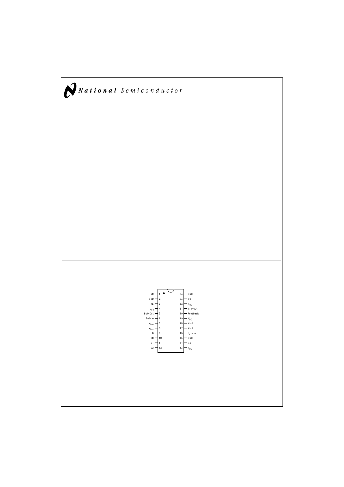
Connection Diagram
Dual-In-Line and
Small Outline Packages
DS012677-2
Top View
Order Number LM4830M
See NS Package Number M24B for SO
Order Number LM4830N
See NS Package Number N24A for DIP
January 1999
LM4830 Two-Way Audio Amplification System with Volume Control
© 1999 National Semiconductor Corporation DS012677 www.national.com
Page 2
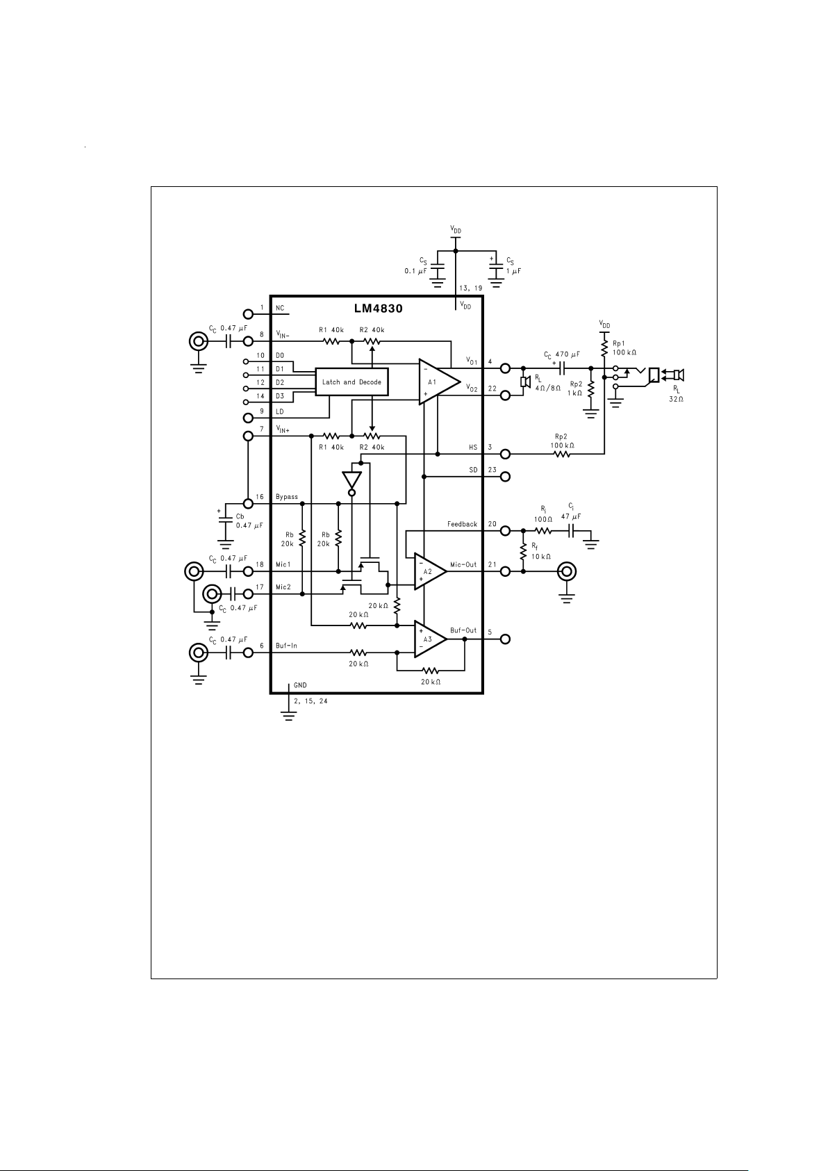
Typical Application
DS012677-1
FIGURE 1. Typical Application Circuit
www.national.com 2
Page 3
Absolute Maximum Ratings (Note 2)
If Military/Aerospace specified devices are required,
please contact the National Semiconductor Sales Office/
Distributors for availability and specifications.
Supply Voltage 6.0V
Storage Temperature −65˚C to +150˚C
Input Voltage −0.3V to V
DD
+ 0.3V
Power Dissipation (Note 3) Internally Limited
ESD Susceptibility (Note 4) 2000V
ESD Susceptibility (Note 5) 250V
Junction Temperature 150˚C
Soldering Information
Small Outline Package
Vapor Phase (60 sec.) 215˚C
Infrared (15 sec.) 220˚C
See AN-450
“Surface Mounting and their Effects on
Product Reliability”
for other methods of soldering surface
mount devices.
Operating Ratings
Temperature Range
T
MIN
≤ TA≤ T
MAX
−40˚C ≤ TA≤ 85˚C
Supply Voltage 2.7V ≤ V
DD
≤ 5.5V
θ
JC
(typ)—M24B 32˚C/W
θ
JA
(typ)—M24B 79˚C/W
θ
JC
(typ)—N24A 21˚C/W
θ
JA
(typ)—N24A 61˚C/W
Electrical Characteristics (Notes 1, 2)
The following specifications apply for V
DD
=
5V, unless otherwise specified. Limits apply for T
A
=
25˚C.
Symbol Parameter Conditions LM4830 Units
(Limits)
Typical Limit
(Note 6) (Note 7)
POWER AMPLIFIER, A1
I
DD
Quiescent Power Supply Current V
O
=
0V, I
O
=
0A, R
L
=
∞
5.8 mA (min)
11.0 20.0 mA (max)
Bridged R
L
=
8Ω 11.4 mA
HS=5V, SD=0V, V
O1
On Only 7.9 mA
I
SD
Shutdown Current HS=5V, SD=5V, IC Off 0.5 2.0 µA (max)
V
OS
Output Offset Voltage V
IN
=
0V 0.7 50.0 mV (max)
e
IN
Input Noise IHF-A Weighting Filter, R
S
=
25Ω
Bridged Output, V
O1–VO2,RL
=
8Ω 30 µV
Single-Ended Output, V
O1,RL
=
32Ω 16 µV
P
O
Output Power, Bridged THD=1%(max); f=1 kHz, R
L
=
8Ω 1.15 1.0 W (min)
THD+N=10%;f=1 kHz, R
L
=
8Ω 1.4 W
THD+N=10%;f=1 kHz, R
L
=
4Ω 2W
THD Total Harmonic Distortion f=1 kHz, Attenuation
@
0dB
P
O
=
1.5W, R
L
=
4Ω 0.2
%
P
O
=
1W, R
L
=
8Ω 0.2
%
V
O1
On Only, V
O
=
60 mV, R
L
=
32Ω 0.06
%
Attenuation Step Size Error 0 dB to −30 dB
±
0.5 dB
Absolute Attenuation Attenuation
@
0dB
±
0.5 dB
Attenuation
@
−30 dB
±
1.0 dB
R
IN
Power Amp Input Resistance 40 kΩ
DIGITAL INPUTS
V
IH
High Input Voltage CMOS Compatible Only 4.5 V
V
IL
Low Input Voltage CMOS Compatible Only 0.5 V
PREAMP, A2
R
IN
Mic1 and Mic2 Input Resistance 21.5 kΩ
V
OS
Output Offset Voltage V
IN
=
0V 2.0 mV
e
IN
Input Noise IHF-A Weighting Filter, R
S
=
25Ω 1.3 10.0 µV (max)
THD Total Harmonic Distortion A
VCL
=
100, V
IN
=
10 mVrms, f=1 kHz 0.06
%
A
VCL
=
−1, P
O
=
50 mW, f=1 kHz, R
L
=
32Ω
0.02
(Refer to
Figure 2
)
www.national.com3
Page 4
Electrical Characteristics (Notes 1, 2) (Continued)
The following specifications apply for V
DD
=
5V, unless otherwise specified. Limits apply for T
A
=
25˚C.
Symbol Parameter Conditions LM4830 Units
(Limits)
Typical Limit
(Note 6) (Note 7)
PREAMP, A2
Xtalk Crosstalk A
VCL
=
100, Power Amp: P
O
=
1W,
R
L
=
8Ω,f=1 kHz
−72 dB
PSRR Power Supply Rejection Ratio V
DDAC
=
0.5 V
PP
,f=1 kHz 60 dB
MICROPHONE BUFFER, A3
R
IN
Buffer Input Resistance 17 kΩ
V
OS
Output Offset Voltage V
IN
=
0V 2.0 mV
e
IN
Input Noise IHF-A Weighting Filter, R
S
=
25Ω 5.8 µV
THD Total Harmonic Distortion P
O
=
50 mW, f=1 kHz, R
L
=
32Ω 0.5
%
Xtalk Crosstalk Power Amp: P
O
=
1W, R
L
=
8Ω,f=1 kHz −76 dB
Note 1: All voltages are measured with respect to the ground pins (Pins 2, 15, and 24), unless otherwise specified.
Note 2: AbsoluteMaximum Ratings indicate limits beyond which damage to the device may occur. Operating Ratings indicate conditions for which the device is func-
tional, but do not guarantee specific performance limits. Electrical Characteristics state DC andAC electrical specifications under particular test conditions which guarantee specific performance limits. This assumes that the device is within the Operating Ratings. Specifications are not guaranteed for parameters where no limit is
given, however, the typical value is a good indication of device performance.
Note 3: The maximum power dissipation must be derated at elevated temperatures and is dictated by T
JMAX
, θJA, and the ambient temperature, TA. The maximum
allowable power dissipation is P
DMAX
=
(T
JMAX−TA
)/θJAor the number given in the Absolute Maximum Ratings, whichever is lower. For the LM4830M, T
JMAX
=
+150˚C, and the typical junction-to-ambient thermal resistance, when board mounted, is 79˚C/W.
Note 4: Human body model, 100 pF discharged through a 1.5 kΩ resistor.
Note 5: Machine model, 200 pF–240 pF discharged through all pins.
Note 6: Typicals are measured at 25˚C and represent the parametric norm.
Note 7: Limits are guarantees that all parts are tested in production to meet the stated values.
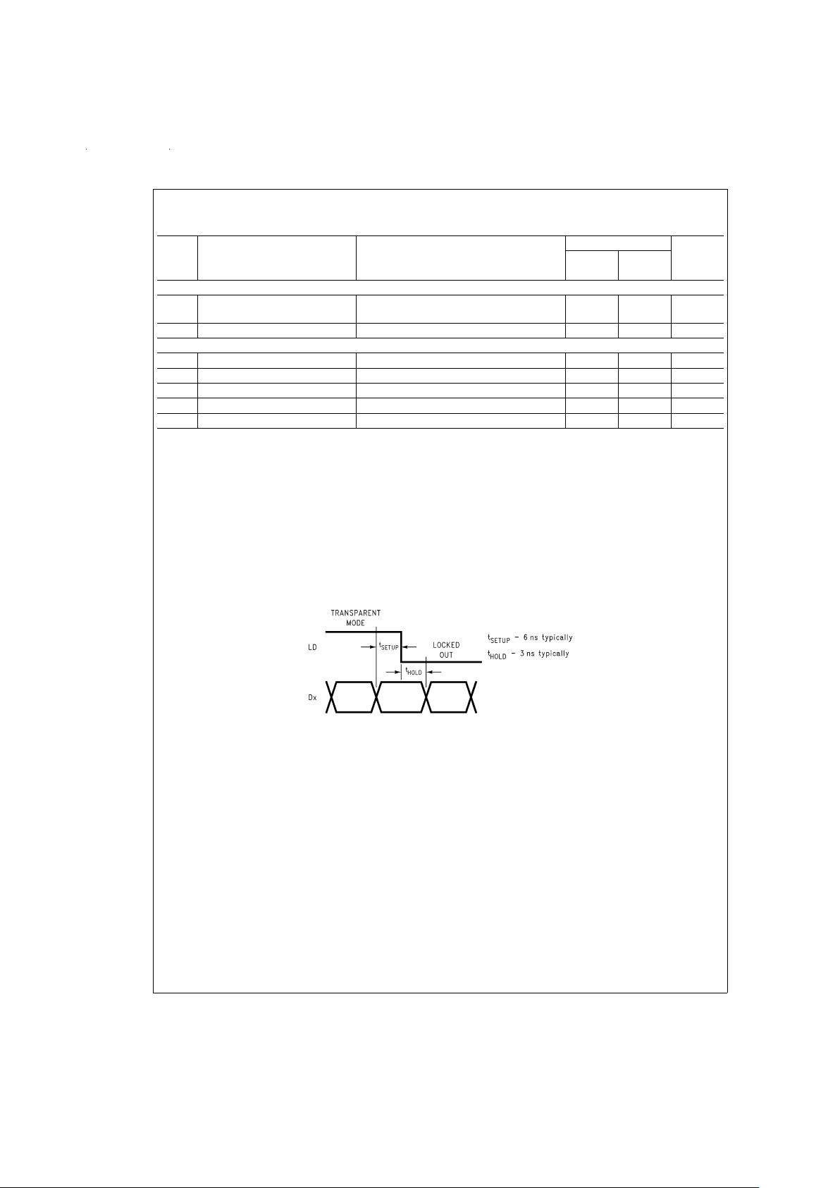
Timing Diagram
DS012677-3
www.national.com 4
Page 5
Computer Application Circuit
DS012677-4
FIGURE 2.
www.national.com5
Page 6

Typical Performance Characteristics (Power Amp-Bridged)
Output Power vs
Supply Voltage
DS012677-5
Wideband Noise Floor
DS012677-6
Frequency Response
vs Attenuation Level
DS012677-7
Output Power vs
Supply Voltage
DS012677-8
Output Power vs
Supply Voltage
DS012677-9
Output Power vs
Supply Voltage
DS012677-10
THD+NvsOutput Power
DS012677-11
THD+NvsOutput Power
DS012677-12
THD+NvsOutput Power
DS012677-13
THD+NvsOutput Power
DS012677-14
THD+NvsOutput Power
DS012677-15
THD+NvsOutput Power
DS012677-16
www.national.com 6
Page 7

Typical Performance Characteristics (Power Amp-Bridged) (Continued)
THD+NvsOutput Power
DS012677-17
THD+NvsOutput Power
DS012677-18
THD+NvsOutput Power
DS012677-19
THD+NvsOutput Power
DS012677-20
THD+NvsOutput Power
DS012677-21
THD+NvsOutput Power
DS012677-22
THD+NvsOutput Power
DS012677-23
THD+NvsFrequency
DS012677-24
THD+NvsFrequency
DS012677-25
THD+NvsOutput Power
DS012677-26
THD+NvsOutput Power
DS012677-27
THD+NvsOutput Power
DS012677-28
www.national.com7
Page 8

Typical Performance Characteristics (Power Amp-Bridged) (Continued)
THD+NvsOutput Power
DS012677-29
Power Amp Crosstalk
to Preamp and Buffer
DS012677-30
Power Amp Crosstalk
to Preamp
DS012677-31
Wideband Noise Floor
DS012677-32
Wideband Noise Floor
DS012677-33
Buffer
Frequency Response
DS012677-34
Output Attenuation
in Shutdown Mode
DS012677-35
Power Dissipation vs
Output Power
DS012677-36
Power Derating Curve
DS012677-37
Supply Current vs
Supply Voltage
DS012677-38
Supply Current vs
Temperature
DS012677-39
Power Supply
Rejection Ratio
DS012677-40
www.national.com 8
Page 9

Application Information
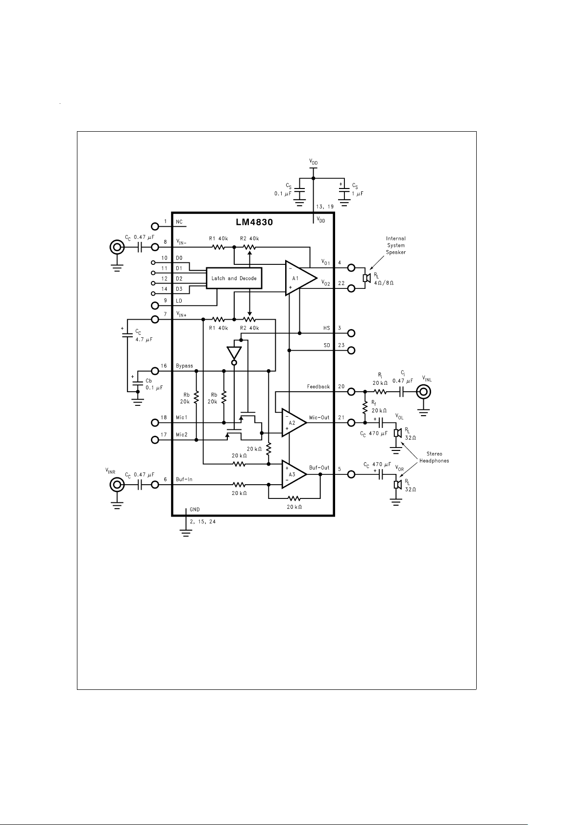
POWER AMPLIFIER HANDSFREE MODE
As shown in
Figure 1
, amplifierA1 can be used in one of two
modes, bridged output or single-ended output. This IC was
intended to be used in systems requiring both internal
speaker drive and external mono-headphone drive capability. Headphones generally have a much higher impedance
than that of speakers since headphones don’t require as
much output power. This also allows headphones to be
driven single-endedly. Shown in
Figure 1
, the output can be
automatically switched from bridged speaker drive to
single-ended headphone drive using a control pin in the
headphone jack that is tied to the Headset (HS) pin, pin 3.
When the voltage at the HS pin input changes from 0V to 5V,
V
O2
of the bridged amplifier output is put into high impedance. This allows the permanently connected internal
speaker of the system to be disabled when a headphone is
plugged into the headphone jack. Output V
O1
then drives the
headphone single-endedly through the output coupling cap,
C
C.CC
should be chosen to allow the full audio bandwidth to
be amplified. Since C
C
and RLcreate a high-pass filter, C
C
must be big enough to allow frequencies down to 20 Hz to be
amplified. The following equation should be used for proper
component selection.
C
C
=
1/(2π(20 Hz)(R
L
)) where 16Ω≤RL≤600Ω (1)
As usual, the output drive limitations are the maximum supply voltage swing, current drive capability, and power dissipation. In bridged-output drive mode, the power amplifier will
drive 4Ω or 8Ω with normal music signals over time. However, trying to put a sinewave through the amplifier at the
worst case power dissipation point could cause the amplifier
to go into thermal shutdown.
In single-ended drive mode, the amplifier is intended to drive
32Ω headphones. It will drive lower impedances with the
limitations of voltage swing and current drive capability. The
result of driving lower impedance loads single-endedly is
lower achievable output power.
Headset and Shutdown Pin Table
HS Pin SD Pin IC Operation Microphone
Low Low All Outputs On MIC1 On
High Low 1/2 A1 On MIC2 On
(V
O1
On Only)
X High Whole IC Off NA
X— “Don’t Care” NA — Not Applicable
POWER DISSIPATION
Power dissipation is a major concern when using any power
amplifier and must be thoroughly understood to ensure a
successful design. Equation 2 states the maximum power
dissipation point for a bridged amplifier operating at a given
supply voltage and driving a specified output load.
P
DMAX
=
4(V
DD
)2/(2π2RL) (2)
Although the LM4830 has three amplifiers in the package,
the bridged amplifier produces the majority of the power dissipation because it supplies the largest amount of output
power. If each of the amplifiers in the LM4830 were of the
same power level, each of their power dissipations would
need to be taken into account. However, this is not the case
and the bridged power amplifier is the only major power dissipation contributor.
Even with the large internal power dissipation created by the
bridged amplifier, the LM4830 does not require heatsinking
over a large range of ambient temperatures. Using Equation
2, assuming a 5V power supply and a 8Ω load, the maximum
power dissipation point is 633 mW.
P
DMAX
=
(T
JMAX−TA
)/θ
JA
(3)
For the LM4830 surface mount package, θ
JA
=
79˚C/W and
T
JMAX
=
150˚C. Depending on the ambient temperature, T
A
,
of the system surroundings, Equation 3 can be used to find
the maximum internal power dissipation supported by the IC
packaging. If the result of Equation 2 is greater than that of
Equation 3, then either the supply voltage must be decreased, the load impedance increased, or the ambient temperature reduced. For the typical application of a 5V power
supply, with a bridged 8Ω load, the maximum ambient temperature possible without violating the maximum junction
temperature is approximately 100˚C provided that device operation is around the maximum power dissipation point. The
average power dissipation caused by typical music material
played at a reasonable level is generally lower than the
maximum power dissipation point. Refer to the Typical Per-
formance Characteristics curves for power dissipation information for lower output powers.
POWER SUPPLY BYPASSING
As with any power amplifier, proper supply bypassing is critical for low noise performance and high power supply rejection. The capacitor location on both the half-supply bypass
and power supply pins should be as close to the device as
possible. The effect of a larger half-supply bypass capacitor
is improved low frequency PSRR due to increased
half-supply stability. Typical applications employ a 5V regulator with 10 µF and a 0.1 µF bypass capacitors which aid in
supply stability, but do not eliminate the need for bypassing
the supply nodes of the LM4830. The selection of bypass capacitors, especially C
b
, is thus dependent upon desired low
frequency PSRR, system cost, and size constraints.
GROUNDING
In order to achieve the best possible performance, there are
certain grounding techniques that should be followed. All input reference grounds should be tied with their respective
source grounds and brought back to the power supply
ground separately from the output load ground returns.
Those input grounds should also be tied in with the
half-supply bypass ground, pin 16. As an example, the AC input ground reference for the power amplifier, A1, is V
IN+
, pin
7. This ground should be tied as close as possible to the Bypass ground (pin 16), as shown in
Figure 1
. In order to tie in
the signal source ground, the audio jack ground on V
IN−
should also be tied to the Bypass ground.
As stated above, the ground returns for the output loads
should be brought back to the supply ground individually.
This will keep large signal currents on those ground lines
from interfering with the stable AC input ground references.
In addition, the signal ground reference for the preamp, A2,
(the ground end of capacitor C
I
) should be tied together with
the mic inputs’ signal ground reference from the microphone.
LAYOUT ISSUES
As stated in the Grounding section, placement of ground return lines is imperative in maintaining the highest level of
system performance. It is not only important to route the correct ground return lines together, but also equally important
to be aware of where those ground return lines are routed in
conjunction with each other. As an example, the output load
www.national.com9
Page 10

Application Information (Continued)
ground return lines should not be tied together with AC input
reference ground return lines. In addition, the layout of these
ground lines should be physically located as far as reasonably possible from each other so that large signal coupling
cannot occur.Tofurther exemplify this point, the outputs and
output load returns for the power amplifier, which have volts
of signal on them, should be physically isolated from the sensitive inputs and AC input ground returns associated with the
preamp. It is easy for large signals to couple into the sensitive low voltage microphone preamp inputs.
TABLE 1. 4-Bit Attenuation Control
LD Input Bits Attenuation Bridge
Pin msb: lsb Level (dB) Amplifier
D3–D0 Gain (dB)
1 0000 0 dB 6 dB
1 0001 −2 dB 4 dB
1 0010 −4 dB 2 dB
1 0011 −6 dB 0 dB
1 0100 −8 dB −2 dB
1 0101 −10 dB −4 dB
1 0110 −12 dB −6 dB
1 0111 −14 dB −8 dB
1 1000 −16 dB −10 dB
1 1001 −18 dB −12 dB
1 1010 −20 dB −14 dB
1 1011 −22 dB −16 dB
1 1100 −24 dB −18 dB
1 1101 −26 dB −20 dB
1 1110 −28 dB −22 dB
1 1111 −30 dB −24 dB
0 XXXX NC NC
0— Logic Low (0V)
1— Logic High (5V)
X— Don’t Care
NC— No Change
DIGITAL ATTENUATION CONTROL
The Load (LD) pin, pin 9, has two modes of operation. When
this input pin is a logic high, 5V,the power amp’s attenuation
control is in “transparent mode” where the voltages on bits
D0–D3 will cause the appropriate attenuation level to be
latched and decoded within the IC. For normal attenuation,
pin 9 should be at 5V. When the LD input pin is a logic low,
0V, the power amp’s attenuation control is “locked-out” so
that any change in the input bits will not cause a subsequent
change in the amp’s attenuation level.
The attenuation level is preset to −16 dB when the IC is first
powered up, assuming that LD is a logic low until the IC is
fully biased up.
To provide the best click and pop performance when changing attenuation levels, each step should be utilized. If a
mute-type function is desired, it is recommended that each
of the attenuation steps be “ramped through” quicker than
the normal attenuation ramp.
To ensure that attenuation steps are flawless when data is
transitioning with load, refer to the timing diagram for proper
setup and hold times.
SELECTION OF EXTERNAL CAPACITORS
The IC’s low frequency power supply rejection can be improved by using a larger bypass capacitor, C
b
. By increasing
this capacitor value, the THD performance at low frequencies will also be improved. For cost sensitive designs, 0.1 µF
is recommended, however, for best performance at least 1
µF should be used.
The selection of the microphone input coupling capacitors
should be based on desired low frequency coupling. Since
the input resistance for those inputs is around 20 kΩ, the
coupling cap should be 0.47 µF for 17 Hz coupling or 0.047
µF for 170 Hz coupling.
Similarly, the selection of the power amplifier input coupling
capacitors should be based on an input resistance of 40 kΩ,
so for flatband 20 Hz reproduction, 0.47 µF caps or larger
should be used.
VOICE-BAND DESIGN
The preamp on this IC is intended to be used for microphone
amplification. Depending upon the frequency response of
the microphone, the preamplifier’s response can be configured to fit the microphone. Simple capacitors can be used to
bandwidth limit the frequency response of the preamplifier
and improve the system’s performance. Once the gain of the
preamp is chosen, the values for the resistors and capacitors
can be selected based upon desired cutoff frequencies using
the equations below.
A
VCL
=
1+R
f/Ri
(4)
flp=1/(2π R
fCf
) (5)
fhp=1/(2π R
iCi
) (6)
As an example, lets assume that the desired closed-loop
gain is 40 dB and the desired voice-band is 300 Hz to 3 kHz.
Using Equation 4, we choose R
f
=
100 kΩ and R
i
=
1kΩ.
The desired value in dB is equal to 20 log (A
VCL
). Then, solv-
ing for C
f
and Ciusing flp=3 kHz, fhp=300 Hz, R
f
=
100
kΩ, and R
i
=
1kΩwe get the following: C
f
=
530 pF and C
i
=
0.53 µF.
COMPUTER APPLICATION CIRCUIT
The LM4830 can also be used to drive both an internal system speaker and stereo headphones simultaneously, as
shown in
Figure 2
. The internally configured unity-gain buffer
requires the preamp to also be set up in an inverting
unity-gain fashion to maintain proper signal phase between
channels for the stereo headphone amplifier. The unity-gain
configured circuit also requires that the AC input signal dynamic range be properly conditioned for the 2.5 V
PK
signal
swing.
Please refer to the Typical Performance Characteristics
curves for THD+N vs P
O
and frequency of the MIC preamp
and buffer.
SHUTDOWN FUNCTION
In order to reduce current consumption while not in use, the
LM4830 contains a shutdown pin to externally turn off the
IC’s bias circuitry. This shutdown feature turns the IC off
when a logic high is placed on the shutdown pin. The trigger
point between a logic low and logic high is typically
half-supply. Quiescent current consumption will depend
upon the value of this voltage. It is best for this voltage to be
forced to V
DD
to obtain the guaranteed shutdown current.
The shutdown feature reduces quiescent supply current consumption from a typical 11 mA to under 2 µA for the whole IC.
www.national.com 10
Page 11

Application Information (Continued)
This feature is especially useful when the IC is used in portable battery operated systems where energy conservation
is imperative.
In many applications, a microcontroller or microprocessor
output interfaces to the LM4830 shutdown pin, providing a
quick, smooth transition into shutdown.Another solution is to
use a single-pole, single-throw switch in conjunction with an
external pull-up resistor. When the switch is closed, the shutdown pin is connected to ground and enables the amplifier. If
the switch is open, the external pull-up resistor disables the
LM4830 by bringing the shutdown pin up to V
DD
. This
scheme guarantees that the shutdown pin will not float, preventing unwanted state changes.
Additionally, when the IC comes out of shutdown the IC’s
volume attenuation setting will remain unchanged.
www.national.com11
Page 12

12
Page 13

Physical Dimensions inches (millimeters) unless otherwise noted
24-Lead (0.300" Wide) Molded Small Outline Package, JEDEC
Order Number LM4830M
NS Package Number M24B
24-Lead (0.600" Wide) Molded Dual-In-Line Package
Order Number LM4830N
NS Package Number N24A
www.national.com13
Page 14

LIFE SUPPORT POLICY
NATIONAL’S PRODUCTS ARE NOT AUTHORIZED FOR USE AS CRITICAL COMPONENTS IN LIFE SUPPORT DEVICES OR SYSTEMS WITHOUT THE EXPRESS WRITTEN APPROVAL OF THE PRESIDENT OF NATIONAL SEMICONDUCTOR CORPORATION. As used herein:
1. Life support devices or systems are devices or systems which, (a) are intended for surgical implant into
the body, or (b) support or sustain life, and whose failure to perform when properly used in accordance
with instructions for use provided in the labeling, can
be reasonably expected to result in a significant injury
to the user.
2. A critical component in any component of a life support
device or system whose failure to perform can be reasonably expected to cause the failure of the life support
device or system, or to affect its safety or effectiveness.
National Semiconductor
Corporation
Americas
Tel: 1-800-272-9959
Fax: 1-800-737-7018
Email: support@nsc.com
www.national.com
National Semiconductor
Europe
Fax: +49 (0) 1 80-530 85 86
Email: europe.support@nsc.com
Deutsch Tel: +49 (0) 1 80-530 85 85
English Tel: +49 (0) 1 80-532 78 32
Français Tel: +49 (0) 1 80-532 93 58
Italiano Tel: +49 (0) 1 80-534 16 80
National Semiconductor
Asia Pacific Customer
Response Group
Tel: 65-2544466
Fax: 65-2504466
Email: sea.support@nsc.com
National Semiconductor
Japan Ltd.
Tel: 81-3-5639-7560
Fax: 81-3-5639-7507
LM4830 Two-Way Audio Amplification System with Volume Control
National does not assume any responsibility for use of any circuitry described, no circuit patent licenses are implied and National reserves the right at any time without notice to change said circuitry and specifications.
 Loading...