

Page 1
LM4819
350mW Audio Power Amplifier with Shutdown Mode
General Description
The LM4819 is a mono bridged power amplifier that is capable of delivering 350mW
RMS
output power into a 16Ω load
or 300mW
RMS
output power into an 8Ω load with 10%
THD+N from a 5V power supply.
The LM4819 Boomer audio power amplifier is designed
specifically to provide high quality output power and minimize PCB area with surface mount packaging and a minimal
amount of external components. Since the LM4819 doesnot
require output coupling capacitors, bootstrap capacitors or
snubber networks, it is optimally suited for low-power portable applications.
The closed loop response of the unity-gain stable LM4819
can be configured using external gain-setting resistors. The
device is available in LLP, MSOP, and SO package types to
suit various applications.
Key Specifications
n THD+N at 1kHz, 350mW continuous average output
power into 16Ω 10% (max)
n THD+N at 1kHz, 300mW continuous average output
power into 8Ω 10% (max)
n Shutdown Current 0.7µA (typ)
Features
n LLP, SOP, and MSOP surface mount packaging.
n Switch on/off click suppression.
n Unity-gain stable.
n Minimum external components.
Applications
n General purpose audio
n Portable electronic devices
n Information Appliances (IA)
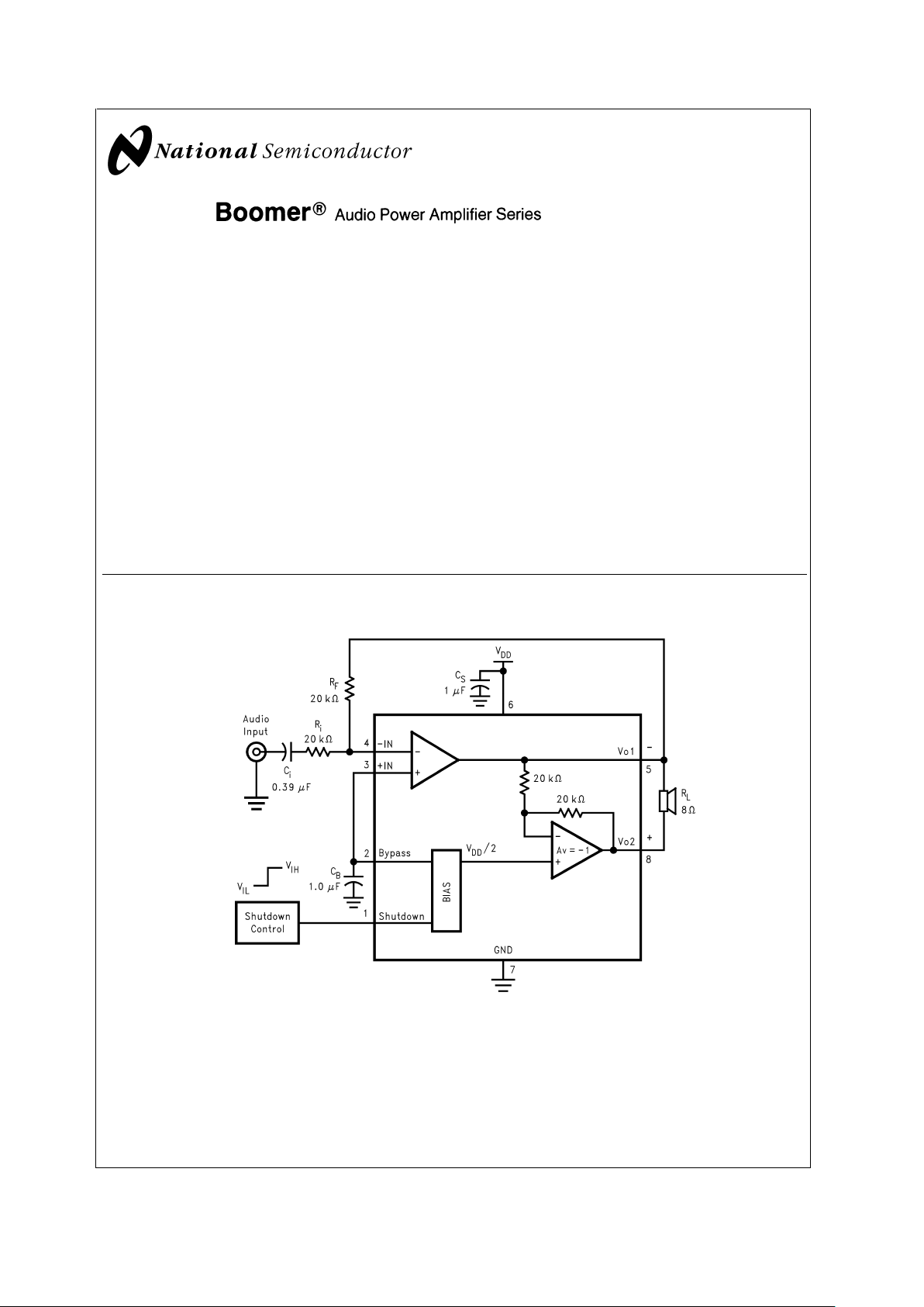
Typical Application
Boomer®is a registered trademark of National Semiconductor Corporation.
DS200136-1
FIGURE 1. Typical Audio Amplifier Application Circuit
April 2002
LM4819 350mW Audio Power Amplifier with Shutdown Mode
© 2002 National Semiconductor Corporation DS200136 www.national.com
Page 2
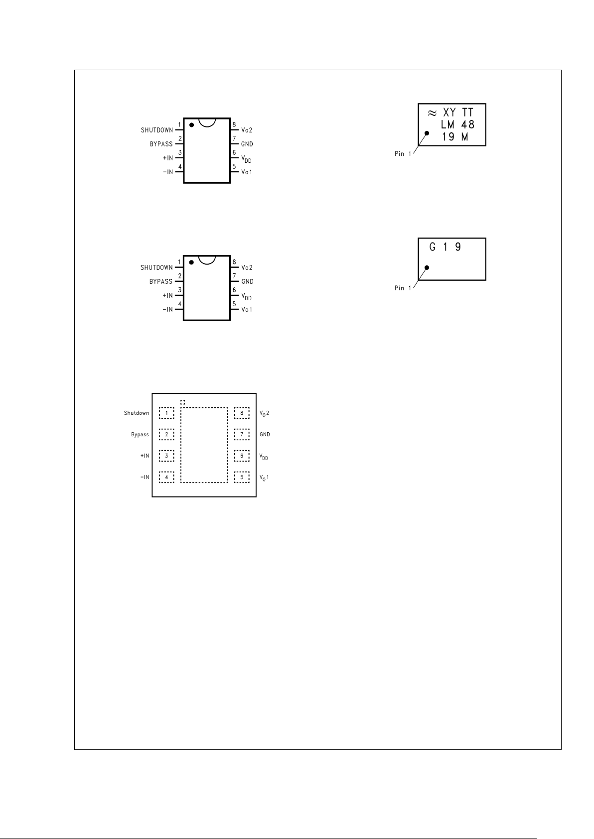
Connection Diagrams
Small Outline (SO) Package
DS200136-35
Top View
Order Number LM4819M
See NS Package Number M08A
Mini Small Outline (MSOP) Package
DS200136-36
Top View
Order Number LM4819MM
See NS Package Number MUA08A
LLP Package
DS200136-74
Top View
Order Number LM4819LD
See NS Package Number LDA08B
SO Marking
DS200136-72
Top View
XY - Date Code
TT - Die Traceability
Bottom 2 lines - Part Number
MSOP Marking
DS200136-71
Top View
G - Boomer Family
19 - LM4819MM
LM4819
www.national.com 2
Page 3
Absolute Maximum Ratings (Notes 2, 3)
If Military/Aerospace specified devices are required,
please contact the National Semiconductor Sales Office/
Distributors for availability and specifications.
Supply Voltage 6.0V
Storage Temperature −65˚C to +150˚C
Input Voltage −0.3V to V
DD
+0.3V
Power Dissipation (P
D
) (Note 4) Internally Limited
ESD Susceptibility (Note 5) 3.5kV
ESD Susceptibility (Note 6) 250V
Junction Temperature (T
J
) 150˚C
Soldering Information (Note 1)
Small Outline Package
Vapor Phase (60 seconds) 215˚C
Infrared (15 seconds) 220˚C
Thermal Resistance
θ
JC
(MSOP) 56˚C/W
θ
JA
(MSOP) 210˚C/W
θ
JC
(SOP) 35˚C/W
θ
JA
(SOP) 170˚C/W
θ
JA
(LLP) 117˚C/W (Note 10)
θ
JA
(LLP) 150˚C/W (Note 11)
Operating Ratings (Notes 2, 3)
Temperature Range
T
MIN
≤ TA≤ T
MAX
−40˚C ≤ TA≤ 85˚C
Supply Voltage 2.0V ≤ V
CC
≤ 5.5V
Electrical Characteristics VDD=5V(Notes 2, 3)
The following specifications apply for V
DD
= 5V, RL=16Ωunless otherwise stated. Limits apply for TA= 25˚C.
Symbol Parameter Conditions
LM4819
Units
(Limits)
Typical Limit
(Note 7) (Notes 8, 9)
I
DD
Quiescent Power Supply Current VIN= 0V, Io= 0A 1.5 3.0 mA (max)
I
SD
Shutdown Current V
PIN1=VDD
(Note 12) 1.0 5.0 µA (max)
V
SDIH
Shutdown Voltage Input High 4.0 V (min)
V
SDIL
Shutdown Voltage Input Low 1.0 V (max)
V
OS
Output Offset Voltage VIN= 0V 5 50 mV (max)
P
O
Output Power
THD = 10%, f
IN
= 1kHz 350 mW
THD = 10%, f
IN
= 1kHz, RL=8Ω 300 mW
THD+N Total Harmonic Distortion + Noise P
O
= 270mW
RMS,AVD
=2,fIN=
1kHz
1%
Electrical Characteristics VDD=3V(Notes 2, 3)
The following specifications apply for V
DD
= 3V and RL=16Ωload unless otherwise stated. Limits apply to TA= 25˚C.
Symbol Parameter Conditions
LM4819
Units
(Limits)
Typical Limit
(Note 7) (Notes 8, 9)
I
DD
Quiescent Power Supply Current VIN= 0V, Io= 0A 1.0 3.0 mA (max)
I
SD
Shutdown Current V
PIN1=VDD
(Note 12) 0.7 5.0 µA (max)
V
SDIH
Shutdown Voltage Input High 2.4 V (min)
V
SDIL
Shutdown Voltage Input Low 0.6 V (max)
V
OS
Output Offset Voltage VIN= 0V 5 50 mV
P
O
Output Power
THD = 10%, f
IN
= 1kHz 110 mW
THD = 10%, f
IN
= 1kHz, RL=8Ω 90 mW
THD+N Total Harmonic Distortion + Noise P
O
= 80mW
RMS,AVD
=2,fIN=
1kHz
1%
LM4819
www.national.com3
Page 4
Electrical Characteristics VDD=3V(Notes 2, 3)
The following specifications apply for V
DD
= 3V and RL=16Ωload unless otherwise stated. Limits apply to TA=
25˚C. (Continued)
Note 1: See AN-450 ’Surface Mounting and their Effects on Product Reliability’ for other methods of soldering surface mount devices.
Note 2: All voltages are measured with respect to the ground pin, unless otherwise specified.
Note 3:
Absolute Maximum Ratings
indicate limits beyond which damage to the device may occur.
Operating Ratings
indicate conditions for which the device is
functional, but do not guarantee specific performance limits.
Electrical Characteristics
state DC and AC electrical specifications under particular test conditions which
guarantee specific performance limits. This assumes that the device is within the Operating Ratings. Specifications are not guaranteed for parameters where no limit
is given. However, the typical value is a good indication of device’s performance.
Note 4: The maximum power dissipation must be derated at elevated temperatures and is dictated by T
JMAX
, θJA, and the ambient temperature TA. The maximum
allowable power dissipation is P
DMAX
=(T
JMAX–TA
)/θJA. For the LM4819, T
JMAX
= 150˚C and the typical junction-to-ambient thermal resistance (θJA) when board
mounted is 210˚C/W for the MSOP package and 170˚C/W for the SOP package.
Note 5: Human body model, 100pF discharged through a 1.5 kΩ resistor.
Note 6: Machine Model, 220pF–240pF capacitor is discharged through all pins.
Note 7: Typical specifications are specified at 25˚C and represent the parametric norm.
Note 8: Tested limits are guaranteed to National’s AOQL (Average Outgoing Quality Level).
Note 9: Datasheet min/max specification limits are guaranteed by designs, test, or statistical analysis.
Note 10: The given θ
JA
is for an LM4819 package in an LDA08B with the Exposed-DAP soldered to a printed circuit board copper pad with an area equivalent to
that of the Exposed-DAP itself. The Exposed-DAP of the LDA08B package should be electrically connected to GND or an electrically isolated copper area.
Note 11: The given θ
JA
is for an LM4819 package in an LDA08B with the Exposed-DAP not soldered to any printed circuit board copper.
Note 12: The shutdown pin (pin1) should be driven as close as possible to V
DD
for minimum current in Shutdown Mode.
External Components Description (
Figure 1
)
Components Functional Description
1. R
i
Combined with Rf, this inverting input resistor sets the closed-loop gain. Rialso forms a high pass filter with
C
i
at fc= 1/(2πRiCi).
2. C
i
This input coupling capacitor blocks DC voltage at the amplifier’s terminals. Combined with Ri, it creates a
high pass filter with R
i
at fc= 1/(2πRiCi). Refer to the section, Proper Selection of External Components
for an explanation of how to determine the value of C
i
.
3. R
f
Combined with Ri, this is the feedback resistor that sets the closed-loop gain: Av= 2(RF/Ri).
4. C
S
This is the power supply bypass capacitor that filters the voltage applied to the power supply pin. Refer to
the Application Information section for proper placement and selection of C
s
.
5. C
B
This is the bypass pin capacitor that filters the voltage at the BYPASS pin. Refer to the section, Proper
Selection of External Components, for information concerning proper placement and selection of C
B
.
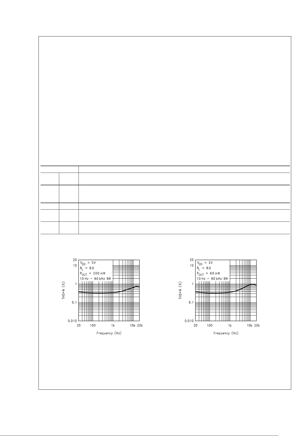
Typical Performance Characteristics
THD+N vs Frequency
DS200136-37
THD+N vs Frequency
DS200136-38
LM4819
www.national.com 4
Page 5
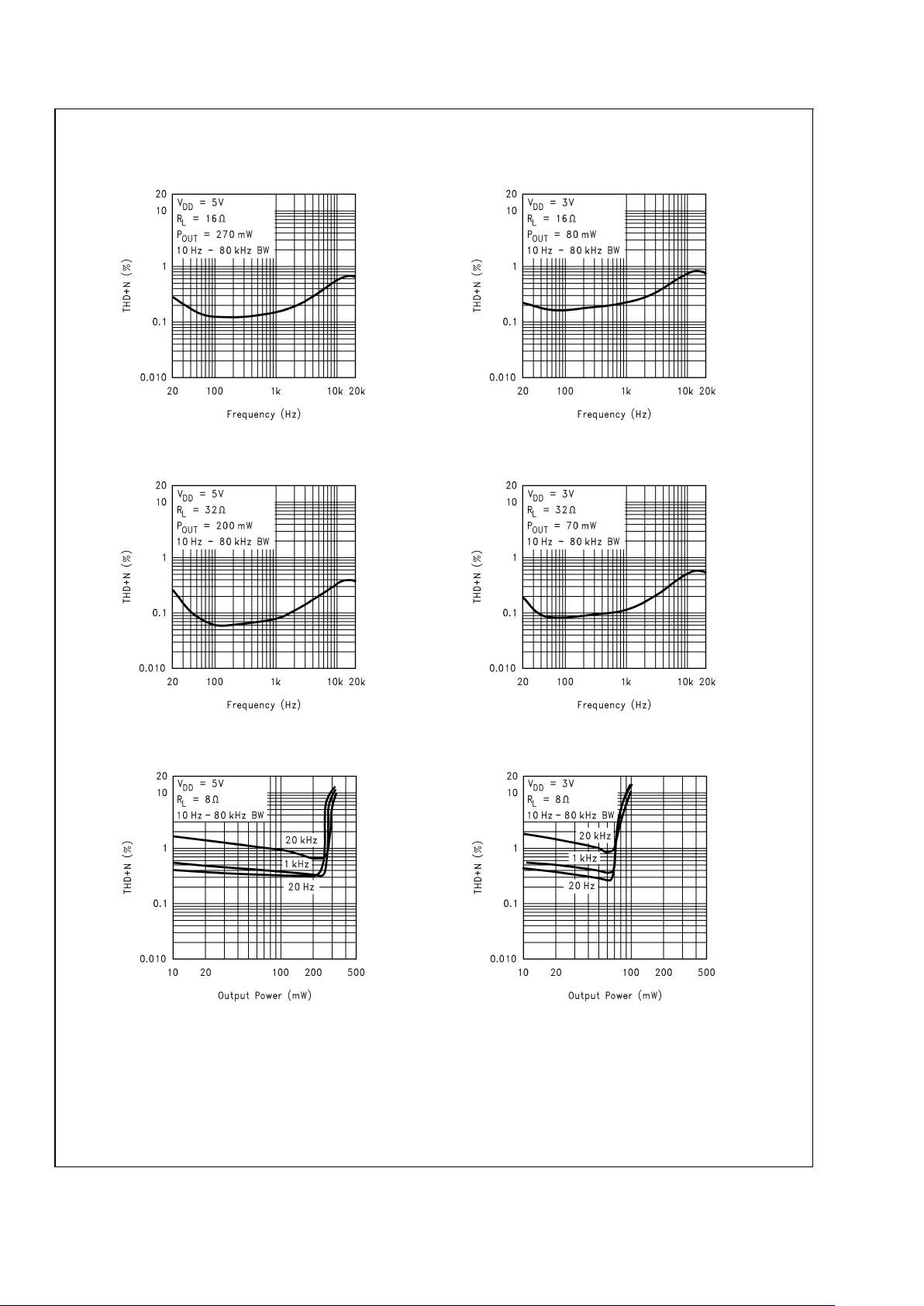
Typical Performance Characteristics (Continued)
THD+N vs Frequency
DS200136-39
THD+N vs Frequency
DS200136-40
THD+N vs Frequency
DS200136-41
THD+N vs Frequency
DS200136-42
THD+N vs Output Power
DS200136-43
THD+N vs Output Power
DS200136-44
LM4819
www.national.com5
Page 6
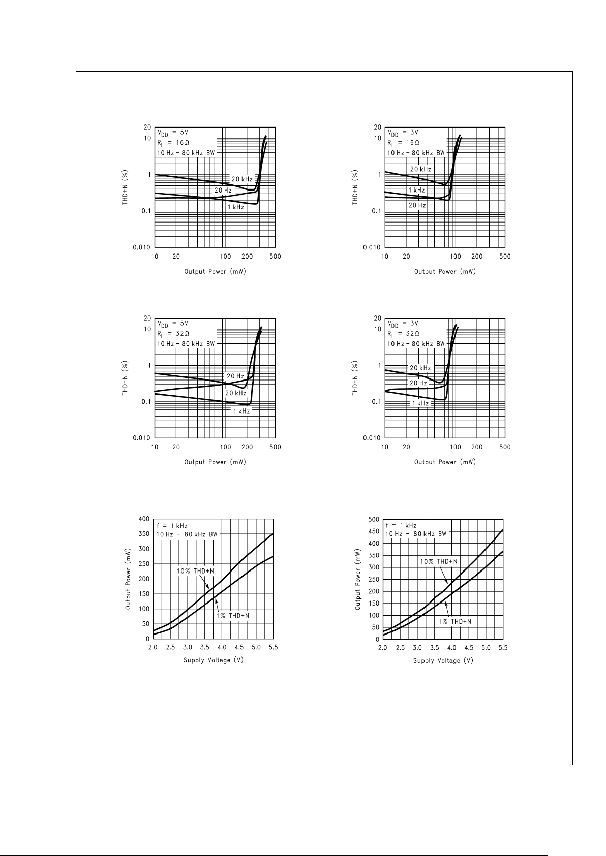
Typical Performance Characteristics (Continued)
THD+N vs Output Power
DS200136-45
THD+N vs Output Power
DS200136-73
THD+N vs Output Power
DS200136-47
THD+N vs Output Power
DS200136-46
Output Power vs Supply Voltage
R
L
=8Ω
DS200136-49
Output Power vs Supply Voltage
R
L
=16Ω
DS200136-48
LM4819
www.national.com 6
Page 7
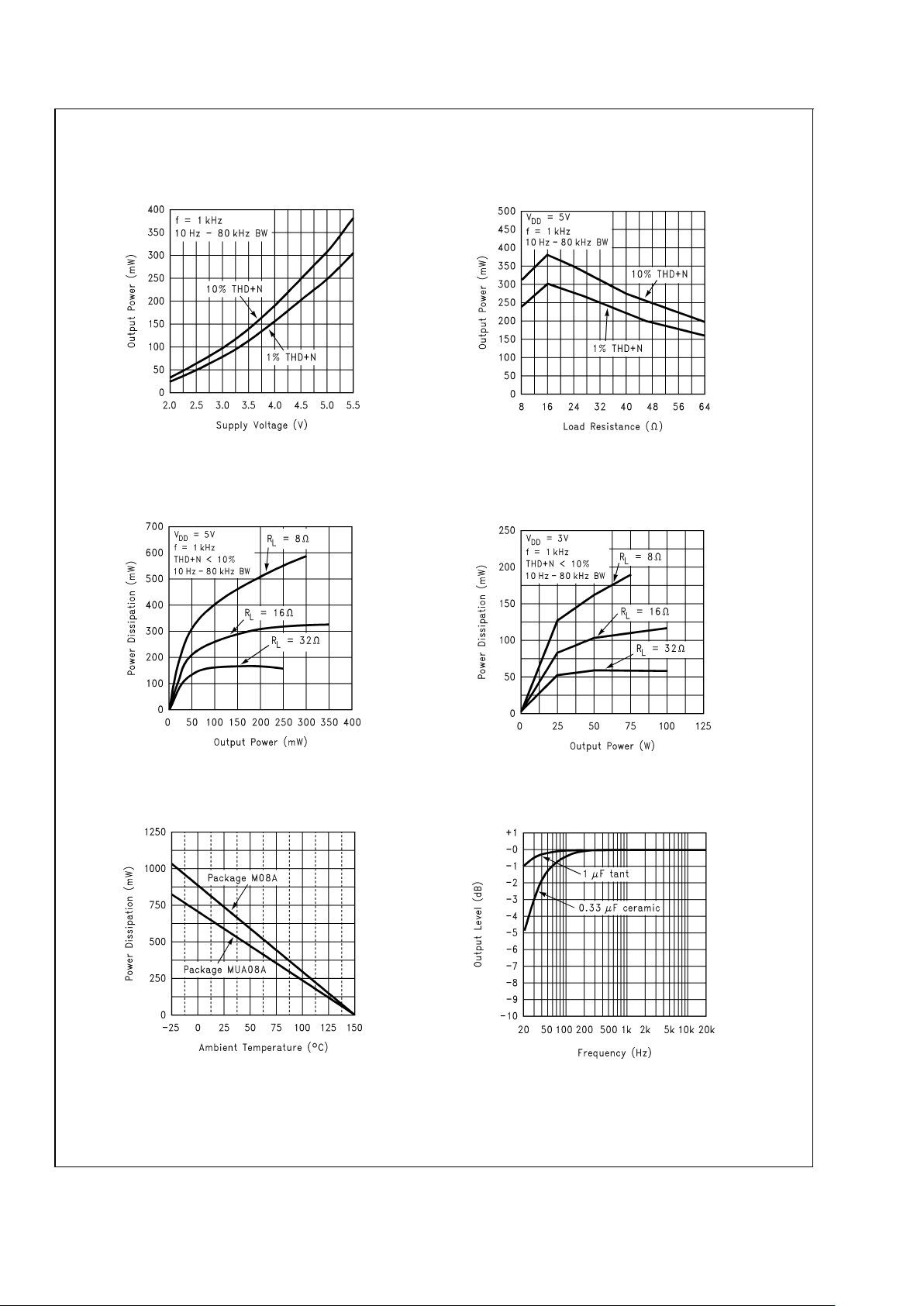
Typical Performance Characteristics (Continued)
Output Power vs Supply Voltage
R
L
=32Ω
DS200136-51
Output Power vs Load Resistance
DS200136-50
Power Dissipation vs
Output Power
V
DD
=5V
DS200136-53
Power Dissipation vs
Output Power
V
DD
=3V
DS200136-52
Power Derating Curves
DS200136-55
Frequency Response vs
Input Capacitor Size
DS200136-54
LM4819
www.national.com7
Page 8

Typical Performance Characteristics (Continued)
Supply Current vs
Supply Voltage
DS200136-69
LM4819
www.national.com 8
Page 9

Application Information
BRIDGE CONFIGURATION EXPLANATION
As shown in
Figure 1
, the LM4819 consist of two operational
amplifiers. External resistors, R
i
and RFset the closed-loop
gain of the first amplifier (and the amplifier overall), whereas
two internal 20kΩ resistors set the second amplifier’s gain at
-1. The LM4819 is typically used to drive a speaker connected between the two amplifier outputs.
Figure 1
shows that the output of Amp1 servers as the input
to Amp2, which results in both amplifiers producing signals
identical in magnitude but 180˚ out of phase. Taking advantage of this phase difference, a load is placed between V
01
and V02and driven differentially (commonly referred to as
’bridge mode’). This results in a differential gain of
A
VD
= 2 *(Rf/Ri) (1)
Bridge mode is different from single-ended amplifiers that
drive loads connected between a single amplifier’s output
and ground. For a given supply voltage, bridge mode has a
distinct advantage over the single-ended configuration: its
differential output doubles the voltage swing across the load.
This results in four times the output power when compared
to a single-ended amplifier under the same conditions. This
increase in attainable output assumes that the amplifier is
not current limited or the output signal is not clipped. To
ensure minimum output signal clipping when choosing an
amplifier’s closed-loop gain, refer to the Audio Power Am-
plifier Design Example section.
Another advantage of the differential bridge output is no net
DC voltage across the load. This results from biasing V
01
and V02at half-supply. This eliminates the coupling capacitor
that single supply, single-ended amplifiers require. Eliminating an output coupling capacitor in a single-ended configuration forces a single supply amplifier’s half-supply bias voltage across the load. The current flow created by the halfsupply bias voltage increases internal IC power dissipation
and may permanently damage loads such as speakers.
POWER DISSIPATION
Power dissipation is a major concern when designing a
successful bridged or single-ended amplifier. Equation (2)
states the maximum power dissipation point for a singleended amplifier operating at a given supply voltage and
driving a specified load.
P
DMAX
=(VDD)2/(2π2RL) (W) Single-ended (2)
However, a direct consequence of the increased power delivered to the load by a bridged amplifier is an increase in the
internal power dissipation point for a bridge amplifier operating at the same given conditions. Equation (3) states the
maximum power dissipation point for a bridged amplifier
operating at a given supply voltage and driving a specified
load.
P
DMAX
= 4(VDD)2/(2π2RL) (W) Bridge Mode (3)
The LM4819 has two operational amplifiers in one package
and the maximum internal power dissipation is four times
that of a single-ended amplifier. However, even with this
substantial increase in power dissipation, the Lm4819 does
not require heatsinking. From Equation (3), assuming a 5V
power supply and an 8Ω load, the maximum power dissipation point is 633mW. The maximum power dissipation point
obtained from Equation (3) must not exceed the power dissipation predicted by Equation (4):
P
DMAX
=(T
JMAX-TA
)/θJA(W) (4)
For the micro MUA08A package, θ
JA
= 210˚C/W, for the
M08A package, θ
JA
= 170˚C/W , and T
JMAX
= 150˚C for the
LM4819. For a given ambient temperature, T
A
, Equation (4)
can be used to find the maximum internal power dissipation
supported by the IC packaging. If the result of Equation (3) is
greater than the result of Equation (4), then decrease the
supply voltage, increase the load impedance, or reduce the
ambient temperature. For a typical application using the
M08A packaged LM4819 with a 5V power supply and an 8Ω
load, the maximum ambient temperature that does not violate the maximum junction temperature is approximately
42˚C. If a MUA08A packaged part is used instead with the
same supply voltage and load, the maximum ambient temperature is 17˚C. In both cases, it is assumed that a device
is a surface mount part operating around the maximum
power dissipation point. The assumption that the device is
operating around the maximum power dissipation point is
incorrect for an 8Ω load. The maximum power dissipation
point occurs when the output power is equal to the maximum
power dissipation or 50% efficiency. The LM4819 is not
capable of the output power level (633mW) required to operate at the maximum power dissipation point for an 8Ω load.
To find the maximum power dissipation, the graph Power
Dissipation vs. Output Power must be used. From the
graph, the maximum power dissipation for an 8Ω load and a
5V supply is approximately 575mW. Substituting this value
back into equation (4) for P
DMAX
and using θJA= 210˚C/W
for the MUA08A package, the maximum ambient temperature is calculated to be 29˚C. Using θ
JA
= 170˚C/W for the
M08A package, the maximum ambient temperature is 52˚C.
Refer to the Typical Performance Characteristics curves
for power dissipation information for lower output powers
and maximum power dissipation for each package at a given
ambient temperature.
POWER SUPPLY BYPASSING
As with any power amplifier, proper supply bypassing is
critical for low noise performance and high power supply
rejection. The capacitors connected to the bypass and power
supply pins should be placed as close to the LM4819 as
possible. The capacitor connected between the bypass pin
and ground improves the internal bias voltage’s stability,
producing improved PSRR. The improvements to PSRR
increase as the bypass pin capacitor value increases. Typical applications employ a 5V regulator with 10µF and 0.1µF
filter capacitors that aid in supply stability. Their presence,
however, does not eliminate the need for bypassing the
supply nodes of the LM4819. The selection of bypass capacitor values, especially C
B
, depends on desired PSRR
requirements, click and pop performance as explained in the
section, Proper Selection of External Components, as
well as system cost and size constraints.
SHUTDOWN FUNCTION
The voltage applied to the LM4819’s SHUTDOWN pin controls the shutdown function. Activate micro-power shutdown
by applying V
DD
to the SHUTDOWN pin. When active, the
LM4819’s micro-power shutdown feature turns off the amplifier’s bias circuitry, reducing the supply current. The logic
threshold is typically 1/2V
DD
. The low 0.7µA typical shutdown current is achieved by applying a voltage that is as
near as V
DD
as possible to the SHUTDOWN pin. A voltage
that is less than V
DD
may increase the shutdown current.
Avoid intermittent or unexpected micro-power shutdown by
ensuring that the SHUTDOWN pin is not left floating but
connected to either V
DD
or GND.
LM4819
www.national.com9
Page 10

Application Information (Continued)
There are a few ways to activate micro-power shutdown.
These included using a single-pole, single-throw switch, a
microcontroller, or a microprocessor. When using a switch,
connect an external 10kΩ to 100kΩ pull-up resistor between
the SHUTDOWN pin and V
DD
. Connect the switch between
the SHUTDOWN pin and ground. Select normal amplifier
operation by closing the switch. Opening the switch connects the shutdown pin to V
DD
through the pull-up resistor,
activating micro-power shutdown. The switch and resistor
guarantee that the SHUTDOWN pin will not float. This prevents unwanted state changes. In a system with a microprocessor or a microcontroller, use a digital output to apply the
control voltage to the SHUTDOWN pin. Driving the SHUTDOWN pin with active circuitry eliminates the pull-up resistor
PROPER SELECTION OF EXTERNAL COMPONENTS
Optimizing the LM4819’s performance requires properly selecting external components. Though the LM4819 operates
well when using external components with wide tolerances,
best performance is achieved by optimizing component values.
The LM4819 is unity gain stable, giving the designer maximum design flexibility. The gain should be set to no more
than a given application requires. This allows the amplifier to
achieve minimum THD+N and maximum signal-to-noise ratio. These parameters are compromised as the closed-loop
gain increases. However, low gain demands input signals
with greater voltage swings to achieve maximum output
power. Fortunately, many signal sources such as audio CODECs have outputs of 1V
RMS
(2.83V
P-P
). Please refer to the
Audio Power Amplifier Design section for more information on selecting the proper gain.
Another important consideration is the amplifier’s close-loop
bandwidth. To a large extent, the bandwidth is dictated by
the choice of external components shown in
Figure 1
. The
input coupling capacitor, C
i
, forms a first order high pass filter
that limits low frequency response. This value should be
chosen based on needed frequency response for a few
distinct reasons discussed below
Input Capacitor Value Selection
Amplifying the lowest audio frequencies requires a high
value input coupling capacitor (C
i
in
Figure 1
). A high value
capacitor can be expensive and may compromise space
efficiency in portable designs. In many cases the speakers
used in portable systems, whether internal or external, have
little ability to reproduce signals below 150Hz. Applications
using speakers with limited frequency response reap little
improvement by using a large input capacitor.
Besides affecting system cost and size, C
i
has an effect on
the LM4819’s click and pop performance. When the supply
voltage is first applied, a transient (pop) is created as the
charge on the input capacitor changes from zero to a quiescent state. The magnitude of the pop is directly proportional
to the input capacitor’s value. Higher value capacitors need
more time to reach a quiescent DC voltage (usually 1/2 V
DD
)
when charged with a fixed current. The amplifier’s output
charges the input capacitor through the feedback resistor,
R
F
. Thus, selecting an input capacitor value that is no higher
than necessary to meet the desired -3dB frequency can
minimize pops.
As shown in
Figure 1
, the input resistor (Ri) and the input
capacitor, C
i
produce a -3dB high pass filter cutoff frequency
that is found using Equation (5).
f
-3dB
= 1/(2 πRiCi) (Hz) (5)
As an example when using a speaker with a low frequency
limit of 150Hz, C
i
, using Equation (5) is 0.063µF. The 0.39µF
C
i
shown in
Figure 1
allows the LM4819 to drive a high
efficiency, full range speaker whose response extends down
to 20Hz.
Besides optimizing the input capacitor value, the bypass
capacitor value, C
B
requires careful consideration. The bypass capacitor’s value is the most critical to minimizing
turn-on pops because it determines how fast the LM4819
turns on. The slower the LM4819’s outputs ramp to their
quiescent DC voltage (nominally 1/2V
DD
), the smaller the
turn-on pop. While the device will function properly (no oscillations or motorboating), with C
B
less than 1.0µF, the
device will be much more susceptible to turn-on clicks and
pops. Thus, a value of C
B
equal to or greater than 1.0µF is
recommended in all but the most cost sensitive designs.
Bypass Capacitor Value Selection
Besides minimizing the input capacitor size, careful consideration should be paid to the value of C
B
, the capacitor
connected to the BYPASS pin. Since C
B
determines how
fast the LM4819 settles to quiescent operation, its value is
critical when minimizing turn-on pops. The slower the
LM4819’s outputs ramp to their quiescent DC voltage (nominally 1/2V
DD
), the smaller the turn-on pop. Choosing C
B
equal to 1.0µF along with a small value of Ci(in the range of
0.1µF to 0.39µF) produces a click-less and pop-less shutdown function. As discussed above, choosing C
i
no larger
than necessary for the desired bandwidth helps minimize
clicks and pops.
Optimizing Click and Pop Reduction Performance
The LM4819 contains circuitry that minimizes turn-on and
shutdown transients or ’clicks and pops’. For this discussion,
turn on refers to either applying the power or supply voltage
or when the shutdown mode is deactivated. While the power
supply is ramping to it’s final value, the LM4819’s internal
amplifiers are configured as unity gain buffers. An internal
current source charges the voltage of the bypass capacitor,
C
B
, connected to the BYPASS pin in a controlled, linear
manner. Ideally, the input and outputs track the voltage
charging on the bypass capacitor. The gain of the internal
amplifiers remains unity until the bypass capacitor is fully
charged to 1/2V
DD
. As soon as the voltage on the bypass
capacitor is stable, the device becomes fully operational.
Although the BYPASS pin current cannot be modified,
changing the size of the bypass capacitor, C
B
, alters the
device’s turn-on time and magnitude of ’clicks and pops’.
Increasing the value of C
B
reduces the magnitude of turn-on
pops. However, this presents a tradeoff: as the size of C
B
increases, the turn-on time (Ton) increases. There is a linear
relationship between the size of C
B
and the turn on time.
Below are some typical turn-on times for various values of
C
B
:
C
B
T
ON
0.01µF 20ms
0.1µF 200ms
0.22µF 440ms
0.47µF 940ms
1.0µF 2S
LM4819
www.national.com 10
Page 11

Application Information (Continued)
In order to eliminate ’clicks and pops’, all capacitors must be
discharged before turn-on. Rapidly switching V
DD
may not
allow the capacitors to fully discharge, which may cause
’clicks and pops’.
AUDIO POWER AMPLIFIER DESIGN EXAMPLE
The following are the desired operational
parameters:
Given:
Power Output 100mW
Load Impedance 16Ω
Input Level 1Vrms (max)
Input Impedance 20kΩ
Bandwidth 100Hz–20kHz
±
0.25dB
The design begins by specifying the minimum supply voltage
necessary to obtain the specified output power. To find this
minimum supply voltage, use the Output Power vs. Supply
Voltagegraph in the Typical Performance Characteristics
section. From the graph for a 16Ω load, (graphs are for 8Ω,
16Ω, and 32Ω loads) the supply voltage for 100mW of output
power with 1% THD+N is approximately 3.15 volts.
Additional supply voltage creates the benefit of increased
headroom that allows the LM4819 to reproduce peaks in
excess of 100mW without output signal clipping or audible
distortion. The choice of supply voltage must also not create
a situation that violates maximum dissipation as explained
above in the Power Dissipation section. For example, if a
3.3V supply is chosen for extra headroom then according to
Equation (3) the maximum power dissipation point with a
16Ω load is 138mW. Using Equation (4) the maximum ambient temperature is 121˚C for the MUA08A package and
126˚C for the M08A package.
After satisfying the LM4819’s power dissipation requirements, the minimum differential gain is found using Equation
(6).
(6)
Thus a minimum gain of 1.27 V/V allows the LM4819 to
reach full output swing and maintain low noise and THD+N
performance. For this example, let A
VD
= 1.27. The amplifi-
er’s overall gain is set using the input (R
i
) and feedback (RF)
resistors. With the desired input impedance set to 20kΩ, the
feedback resistor is found using Equation (7).
R
F/Ri=AVD
/2 (V/V) (7)
The value of R
F
is 13kΩ.
The last step in this design example is setting the amplifier’s
-3dB frequency bandwidth. To achieve the desired
±
0.25dB
pass band magnitude variation limit, the low frequency response must extend to at least one-fifth the lower bandwidth
limit and the high frequency response must extend to at least
five times the upper bandwidth limit. The gain variation for
both response limits is 0.17dB, well with in the
±
0.25dB
desired limit.
The results are:
f
L
= 100Hz/5 = 20Hz
f
H
= 20 kHz*5 = 100kHz
As mentioned in the External Components section, R
i
and
C
i
create a high pass filter that sets the amplifier’s lower
band pass frequency limit. Find the coupling capacitor’s
value using Equation (8).
C
i
≥ 1/(2πRifc) (F) (8)
C
i
≥ 0.398µF, a standard value of 0.39µF will be used. The
product of the desired high frequency cutoff (100kHz in this
example) and the differential gain, A
VD
, determines the up-
per pass band response limit. With A
VD
= 1.27 and fH=
100kHz, the closed-loop gain bandwidth product (GBWP) is
127kHz. This is less than the LM4819’s 900kHz GBWP.With
this margin the amplifier can be used in designs that require
more differential gain while avoiding performance restricting
bandwidth limitations.
LM4819
www.national.com11
Page 12

Application Information (Continued)
HIGHER GAIN AUDIO AMPLIFIER
The LM4819 is unity-gain stable and requires no external
components besides gain-setting resistors, an input coupling
capacitor, and proper supply bypassing in the typical application. However, if a closed-loop differential gain of greater
than 10 is required, a feedback capacitor (C
4
) may be
needed as shown in Figure 2 to bandwidth limit the amplifier.
This feedback capacitor creates a low pass filter that eliminates possible high frequency oscillations. Care should be
taken when calculating the -3dB frequency in that an incorrect combination of R
3
and C4will cause rolloff before
20kHz. A typical combination of feedback resistor and capacitor that will not produce audio band high frequency rolloff
is R
3
= 20kΩ and C4= 25pF. These components result in a
-3dB point of approximately 320 kHz. It is not recommended
that the feedback resistor and capacitor be used to implement a band limiting filter below 100kHz.
DS200136-24
Figure 2
LM4819
www.national.com 12
Page 13

Application Information (Continued)
DIFFERENTIAL AMPLIFIER CONFIGURATION FOR LM4819
DS200136-29
Figure 3
LM4819
www.national.com13
Page 14

Application Information (Continued)
REFERENCE DESIGN BOARD and PCB LAYOUT GUIDELINES
DS200136-68
Figure 4
LM4819
www.national.com 14
Page 15

Application Information (Continued)
LM4819 SO DEMO BOARD ARTWORK
Silk Screen
DS200136-62
Top Layer
DS200136-63
Bottom Layer
DS200136-64
LM4819
www.national.com15
Page 16

Application Information (Continued)
LM4819 MSOP DEMO BOARD ARTWORK
Silk Screen
DS200136-65
Top Layer
DS200136-66
Bottom Layer
DS200136-67
LM4819
www.national.com 16
Page 17

Application Information (Continued)
LM4819 LD DEMO BOARD ARTWORK
Composite View
DS200136-31
Silk Screen
DS200136-32
Top Layer
DS200136-33
Bottom Layer
DS200136-30
LM4819
www.national.com17
Page 18

Application Information (Continued)
Mono LM4819 Reference Design Boards
Bill of Material for all Demo Boards
Item Part Number Part Description Qty Ref Designator
1 551011208-001 LM4819 Mono Reference Design Board 1
10 482911183-001 LM4819 Audio AMP 1 U1
20 151911207-001 Tant Cap 1uF 16V 10 1 C1
21 151911207-002 Cer Cap 0.39uF 50V Z5U 20% 1210 1 C2
25 152911207-001 Tant Cap 1uF 16V 10 1 C3
30 472911207-001 Res 20K Ohm 1/10W 5 3 R1, R2, R3
35 210007039-002 Jumper Header Vertical Mount 2X1
0.100
2 J1, J2
PCB LAYOUT GUIDELINES
This section provides practical guidelines for mixed signal
PCB layout that involves various digital/analog power and
ground traces. Designers should note that these are only
’rule-of-thumb’ recommendations and the actual results will
depend heavily on the final layout.
General Mixed Signal Layout Recommendation
Power and Ground Circuits
For two layer mixed signal design, it is important to isolate
the digital power and ground trace paths from the analog
power and ground trace paths. Star trace routing techniques
(bringing individual traces back to a central point rather than
daisy chaining traces together in a serial manner) can have
a major impact on low level signal performance. Star trace
routing refers to using individual traces to feed power and
ground to each circuit or even device. This technique will
take require a greater amount of design time but will not
increase the final price of the board. The only extra parts
required will be some jumpers.
Single-Point Power / Ground Connections
The analog power traces should be connected to the digital
traces through a single point (link). A ’Pi-filter’can be helpful
in minimizing high frequency noise coupling between the
analog and digital sections. It is further recommended to put
digital and analog power traces over the corresponding digital and analog ground traces to minimize noise coupling.
Placement of Digital and Analog Components
All digital components and high-speed digital signals traces
should be located as far away as possible from analog
components and circuit traces.
Avoiding Typical Design / Layout Problems
Avoid ground loops or running digital and analog traces
parallel to each other (side-by-side) on the same PCB layer.
When traces must cross over each other do it at 90 degrees.
Running digital and analog traces at 90 degrees to each
other from the top to the bottom side as much as possible will
minimize capacitive noise coupling and cross talk.
LM4819
www.national.com 18
Page 19

Physical Dimensions inches (millimeters) unless otherwise noted
MSOP
Order Number LM4819MM
NS Package Number MUA08A
LM4819
www.national.com19
Page 20

Physical Dimensions inches (millimeters) unless otherwise noted (Continued)
SO
Order Number LM4819M
NS Package Number M08A
LM4819
www.national.com 20
Page 21

Physical Dimensions inches (millimeters) unless otherwise noted (Continued)
LIFE SUPPORT POLICY
NATIONAL’S PRODUCTS ARE NOT AUTHORIZED FOR USE AS CRITICAL COMPONENTS IN LIFE SUPPORT
DEVICES OR SYSTEMS WITHOUT THE EXPRESS WRITTEN APPROVAL OF THE PRESIDENT AND GENERAL
COUNSEL OF NATIONAL SEMICONDUCTOR CORPORATION. As used herein:
1. Life support devices or systems are devices or
systems which, (a) are intended for surgical implant
into the body, or (b) support or sustain life, and
whose failure to perform when properly used in
accordance with instructions for use provided in the
labeling, can be reasonably expected to result in a
significant injury to the user.
2. A critical component is any component of a life
support device or system whose failure to perform
can be reasonably expected to cause the failure of
the life support device or system, or to affect its
safety or effectiveness.
National Semiconductor
Corporation
Americas
Email: support@nsc.com
National Semiconductor
Europe
Fax: +49 (0) 180-530 85 86
Email: europe.support@nsc.com
Deutsch Tel: +49 (0) 69 9508 6208
English Tel: +44 (0) 870 24 0 2171
Français Tel: +33 (0) 1 41 91 8790
National Semiconductor
Asia Pacific Customer
Response Group
Tel: 65-2544466
Fax: 65-2504466
Email: ap.support@nsc.com
National Semiconductor
Japan Ltd.
Tel: 81-3-5639-7560
Fax: 81-3-5639-7507
www.national.com
LLP
Order Number LM4819LD
NS Package Number LDA08B
LM4819 350mW Audio Power Amplifier with Shutdown Mode
National does not assume any responsibility for use of any circuitry described, no circuit patent licenses are implied and National reserves the right at any time without notice to change said circuitry and specifications.
 Loading...