

Page 1
LM4811
Dual 105mW Headphone Amplifier with Digital Volume
Control and Shutdown Mode
General Description
The LM4811 is a dual audio power amplifier capable of
delivering 105mW per channel of continuous average power
into a 16Ω load with 0.1% (THD+N) from a 5V power supply.
Boomer audio power amplifiers were designed specifically to
provide high quality output power with a minimal amount of
external components. Since the LM4811 does not require
bootstrap capacitors or snubber networks, it is optimally
suited for low-power portable systems.
The LM4811 features a digital volume control that sets the
amplifier’s gain from +12dB to −33dB in 16 discrete steps
using a two−wire interface.
The unity-gain stable LM4811 also features an externally
controlled, active-high, micropower consumption shutdown
mode. It also has an internal thermal shutdown protection
mechanism.
Key Specifications
n THD+N at 1kHz, 105mW continuous average output
power into 16Ω 0.1% (typ)
n THD+N at 1kHz, 70mW continuous average power into
32Ω 0.1% (typ)
n Shutdown Current 0.3µA (typ)
Features
n Digital volume control range from +12dB to −33dB
n LD and MSOP surface mount packaging
n "Click and Pop" suppression circuitry
n No bootstrap capacitors required
n Low shutdown current
Applications
n Cellular Phones
n MP3, CD, DVD players
n PDA’s
n Portable electronics
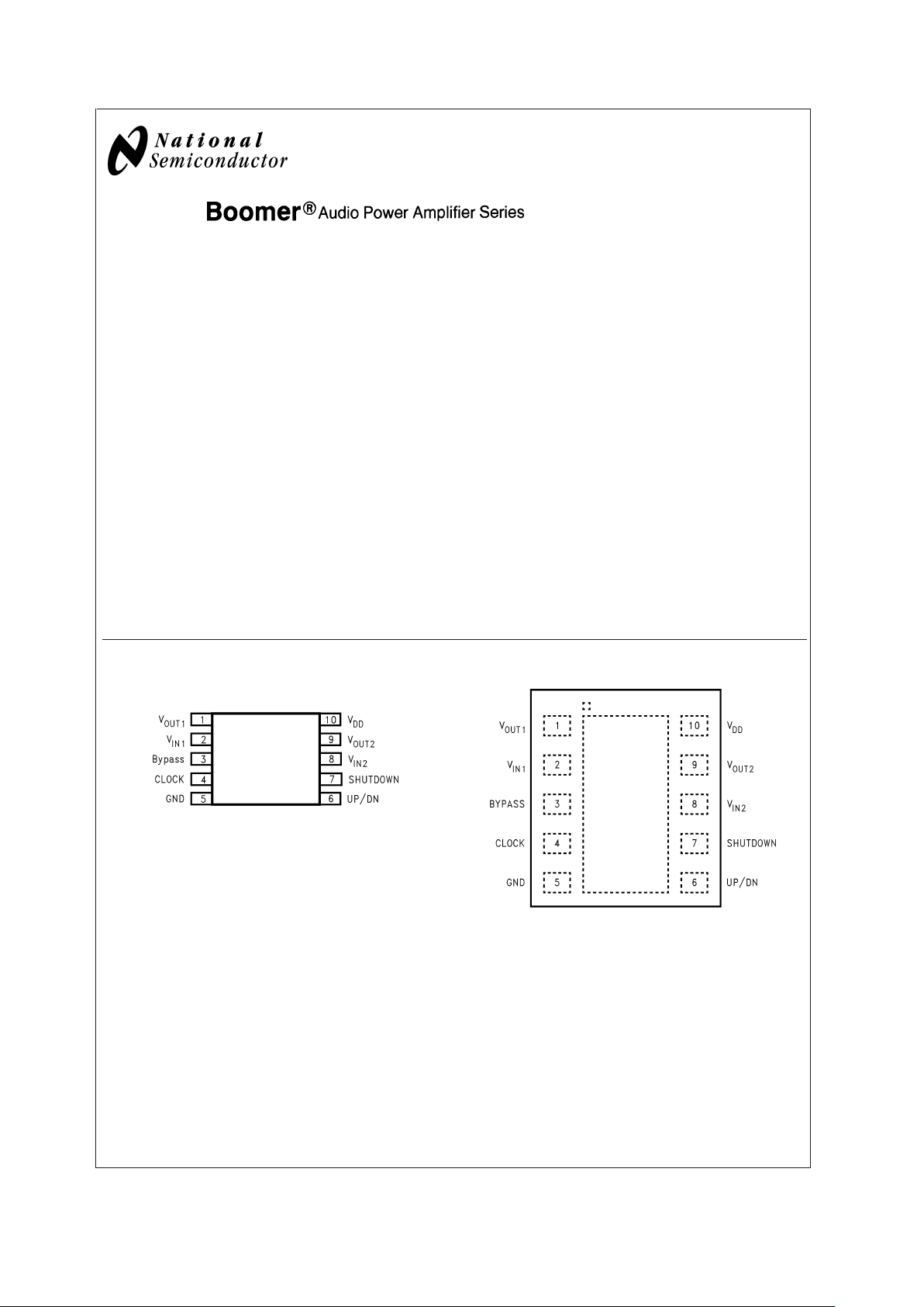
Connection Diagrams
MSOP Package
20006102
Top View
Order Number LM4811MM
See NS Package Number MUB10A
LD Package
20006162
Top View
Order Number LM4811LD
See NS Package Number LDA10A
Boomer®is a registered trademark of National Semiconductor Corporation.
December 2002
LM4811 Dual 105mW Headphone Amplifier with Digital Volume Control and Shutdown Mode
© 2002 National Semiconductor Corporation DS200061 www.national.com
Page 2
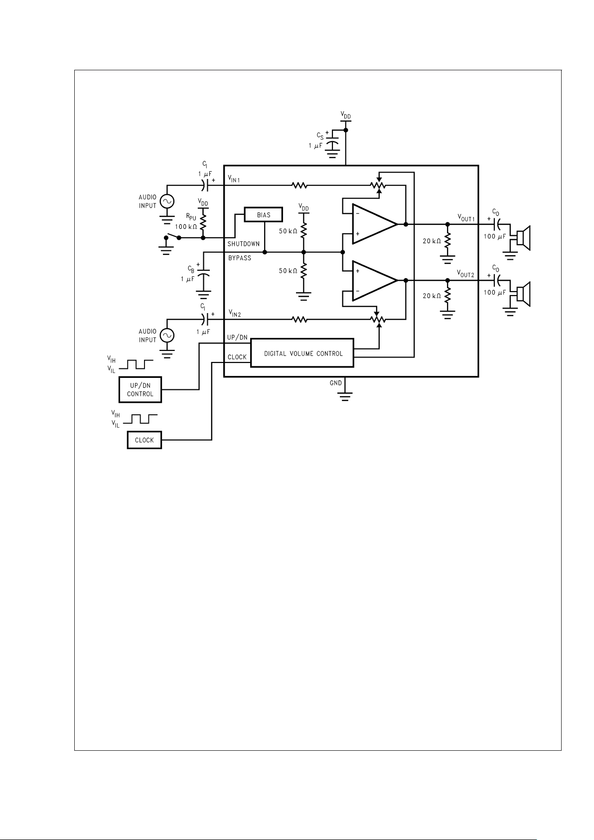
Typical Application
20006101
*Refer to the Application Information Section for information concerning proper selection of the input and output coupling capacitors.
FIGURE 1. Typical Audio Amplifier Application Circuit
LM4811
www.national.com 2
Page 3
Absolute Maximum Ratings (Note 1)
If Military/Aerospace specified devices are required,
please contact the National Semiconductor Sales Office/
Distributors for availability and specifications.
Supply Voltage 6.0V
Storage Temperature −65˚C to +150˚C
ESD Susceptibility (Note 3) 2.5kV
ESD Susceptibility Machine model
(Note 6) 200V
Junction Temperature (T
J
) 150˚C
Soldering Information
Small Outline Package
Vapor Phase (60 sec.) 215˚C
Infrared (15 sec.) 220˚C
Thermal Resistance
θ
JA
MUB10A 194˚C/W
θ
JC
MUB10A 52˚C/W
θ
JA
LDA10A (Note 7) 63˚C/W
θ
JC
LDA10A (Note 7) 12˚C/W
Operating Ratings
Temperature Range
T
MIN
≤ TA≤ T
MAX
−40˚C ≤ TA≤ 85˚C
Supply Voltage 2.0V ≤ V
CC
≤ 5.5V
Electrical Characteristics (Notes 1, 8)
The following specifications apply for VDD= 5V unless otherwise specified, limits apply to TA= 25˚C.
Symbol Parameter Conditions LM4811 Units
(Limits)
Typical
(Note 4)
Limit
(Note 5)
V
DD
Supply Voltage 2.0 V (min)
5.5 V (max)
I
DD
Supply Current VIN= 0V, IO= 0A 1.3 3.0 mA
I
SD
Shutdown Current VIN= 0V 0.3 µA
V
OS
Output Offset Voltage VIN= 0V 4.0 50 mV
P
O
Output Power 0.1% THD+N; f = 1kHz
R
L
=16Ω 105 mW
R
L
=32Ω 70 mW
THD+N Total Harmonic Distortion P
O
= 50mW, RL=32Ω
f = 20Hz to 20kHz
0.3 %
Crosstalk Channel Separation R
L
=32Ω; f = 1kHz;
P
O
= 70mW
100 dB
PSRR Power Supply Rejection Ratio C
B
= 1.0µF, V
RIPPLE
= 100mV
PP
f = 217Hz
60 dB
V
IH
(CLOCK, UP/DN, SHUTDOWN)
Input Voltage High
1.4 V (min)
V
IL
(CLOCK, UP/DN, SHUTDOWN)
Input Voltage Low
0.4 V (max)
Digital Volume Range Input referred minimum gain −33 dB
Input referred maximum gain +12 dB
Digital Volume Stepsize All 16 discrete steps 3.0 dB
Stepsize Error All 16 discrete steps
±
0.3 dB
Channel−to−Channel Volume
Tracking Error
All gain settings from
−33dB to +12dB
0.15 dB
Shutdown Attenuation Shutdown mode active −100 dB
LM4811
www.national.com3
Page 4
Electrical Characteristics (Notes 1, 8)
The following specifications apply for VDD= 3.3V unless otherwise specified, limits apply to TA= 25˚C.
Symbol Parameter Conditions LM4811 Units
(Limits)
Typical
(Note 4)
Limit
(Note 5)
I
DD
Supply Current VIN= 0V, IO= 0A 1.1 mA
I
SD
Shutdown Current VIN= 0V 0.3 µA
V
OS
Output Offset Voltage VIN= 0V 4.0 mV
P
o
Output Power 0.1% THD+N; f = 1kHz
R
L
=16Ω 40 mW
R
L
=32Ω 28 mW
THD+N Total Harmonic Distortion P
O
= 25mW, RL=32Ω
f = 20Hz to 20kHz
0.5 %
PSRR Power Supply Rejection Ratio C
B
= 1.0µF, V
RIPPLE
= 100mV
PP
f = 217Hz
60 dB
V
IH
(CLOCK, UP/DN, SHUTDOWN)
Input Voltage High
1.4 V (min)
V
IL
(CLOCK, UP/DN, SHUTDOWN)
Input Voltage Low
0.4 V (max)
Digital Volume Range Input referred minimum gain −33 dB
Input referred maximum gain +12 dB
Digital Volume Stepsize All 16 discrete steps 3.0 dB
Stepsize Error All 16 discrete steps
±
0.3 dB
Channel−to−Channel Volume
Tracking Error
All gain settings from
−33dB to +12dB
0.15 dB
Shutdown Attenuation Shutdown mode active −100 dB
Electrical Characteristics (Notes 1, 8)
The following specifications apply for VDD= 2.6V unless otherwise specified, limits apply to TA= 25˚C.
Symbol Parameter Conditions LM4811 Units
(Limits)
Typical
(Note 4)
Limit
(Note 5)
I
DD
Supply Current VIN= 0V, IO= 0A 1.0 mA
I
SD
Shutdown Current VIN= 0V 0.3 µA
V
OS
Output Offset Voltage VIN= 0V 4.0 mV
P
o
Output Power 0.1% THD+N; f = 1kHz
R
L
=16Ω 20 mW
R
L
=32Ω 16 mW
THD+N Total Harmonic Distortion P
O
= 15mW, RL=32Ω
f = 20Hz to 20kHz
0.6 %
PSRR Power Supply Rejection Ratio C
B
= 1.0µF, V
RIPPLE
= 100mV
PP
f = 217Hz
60 dB
V
IH
(CLOCK, UP/DN, SHUTDOWN)
Input Voltage High
1.4 V (min)
V
IL
(CLOCK, UP/DN, SHUTDOWN)
Input Voltage Low
0.4 V (max)
Digital Volume Range Input referred minimum gain −33 dB
Input referred maximum gain +12 dB
Digital Volume Stepsize All 16 discrete steps 3.0 dB
Stepsize Error All 16 discrete steps
±
0.3 dB
Channel−to−Channel Volume
Tracking Error
All gain settings from
−33dB to +12dB
0.15 dB
LM4811
www.national.com 4
Page 5
Electrical Characteristics (Notes 1, 8) (Continued)
The following specifications apply for VDD= 2.6V unless otherwise specified, limits apply to TA= 25˚C.
Symbol Parameter Conditions LM4811 Units
(Limits)
Typical
(Note 4)
Limit
(Note 5)
Shutdown Attenuation Shutdown mode active −75 dB
Note 1: Absolute Maximum Ratings indicate limits beyond which damage to the device may occur.
Note 2: Operating Ratings indicate conditions for which the device is functional, but do not guarantee specific performance limits. For guaranteed specifications and
test conditions, see the Electrical Characteristics. The guaranteed specifications apply only for the test conditions listed. Some performance characteristics may
degrade when the device is not operated under the listed test conditions.
Note 3: Human body model, 100pF discharged through a 1.5kΩ resistor.
Note 4: Typical specifications are specified at +25˚C and represent the most likely parametric norm.
Note 5: Tested limits are guaranteed to National’s AOQL (Average Outgoing Quality Level). Datasheet min/max specification limits are guaranteed by design, test,
or statistical analysis.
Note 6: : Machine Model ESD test is covered by specification EIAJ IC-121-1981. A 200pF cap is charged to the specified voltage, then discharged directly into the
IC with no external series resistor (resistance of discharge path must be under 50 Ohms).
Note 7: The LDA10A package has its Exposed−DAP soldered to an exposed 2in
2
area of 1oz printed circuit board copper.
Note 8: All voltages are measured with respect to the ground pin, unless otherwise specified.
External Components Description
(Figure 1)
Components Functional Description
1. C
i
This is the input coupling capacitor. It blocks the DC voltage at, and couples the input signal to, the
amplifier’s input terminals. C
i
also creates a highpass filter with the internal input resistor, Ri,atfc=
1/(2πR
iCi
). The minimum value of Riis 33kΩ. Refer to the section, Proper Selection of External
Components, for an explanation of how to determine the value of C
i
.
2. C
S
This is the supply bypass capacitor. It provides power supply filtering. Refer to the Application
Information section for proper placement and selection of the supply bypass capacitor.
3. C
B
This is the BYPASS pin capacitor. It provides half-supply filtering. Refer to the section, Proper
Selection of External Components, for information concerning proper placement and selection of C
B
.
4. C
O
This is the output coupling capacitor. It blocks the DC voltage at the amplifier’s output and it forms a
high pass filter with R
L
at fO= 1/(2πRLCO)
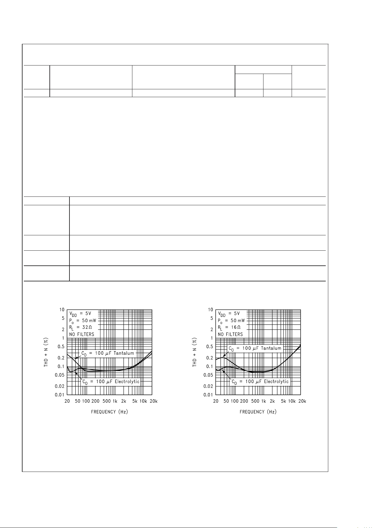
Typical Performance Characteristics
THD+N vs Frequency THD+N vs Frequency
20006103 20006104
LM4811
www.national.com5
Page 6
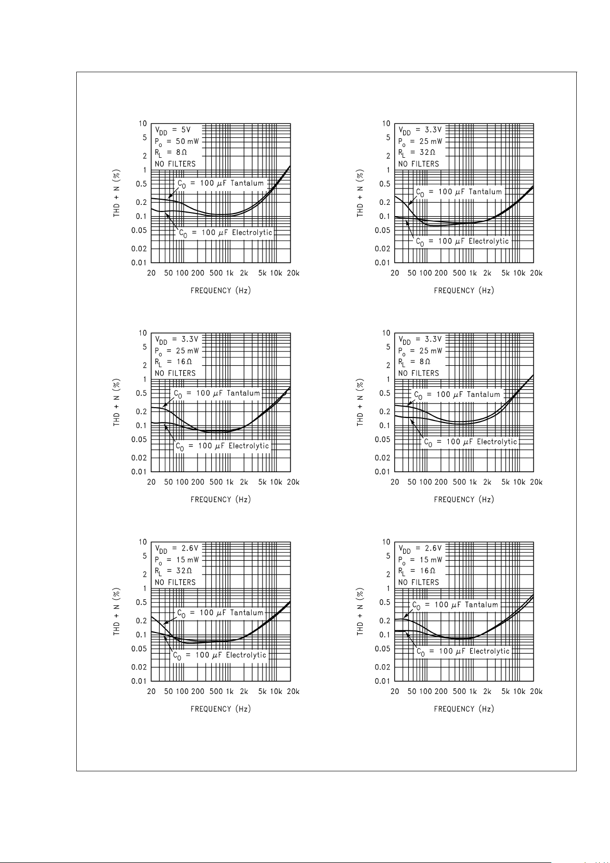
Typical Performance Characteristics (Continued)
THD+N vs Frequency THD+N vs Frequency
20006105 20006106
THD+N vs Frequency THD+N vs Frequency
20006107 20006108
THD+N vs Frequency THD+N vs Frequency
20006109 20006110
LM4811
www.national.com 6
Page 7

Typical Performance Characteristics (Continued)
THD+N vs Frequency THD+N vs Output Power
20006111 20006112
THD+N vs Output Power THD+N vs Output Power
20006113 20006114
THD+N vs Output Power THD+N vs Output Power
20006115 20006116
LM4811
www.national.com7
Page 8

Typical Performance Characteristics (Continued)
THD+N vs Output Power THD+N vs Output Power
20006117 20006118
THD+N vs Output Power THD+N vs Output Power
20006119 20006120
Output Power vs
Load Resistance
Output Power vs
Load Resistance
20006122 20006123
LM4811
www.national.com 8
Page 9

Typical Performance Characteristics (Continued)
Output Power vs
Load Resistance
Output Power vs
Supply Voltage
20006124 20006125
Output Power vs
Power Supply
Output Power vs
Power Supply
20006126 20006127
Dropout Voltage vs
Supply Voltage
Power Dissipation vs
Output Power
20006128
20006129
LM4811
www.national.com9
Page 10

Typical Performance Characteristics (Continued)
Power Dissipation vs
Output Power
Power Dissipation vs
Output Power
20006130
20006131
Channel Separation Channel Separation
20006132 20006133
Noise Floor Power Supply Rejection Ratio
20006134
20006135
LM4811
www.national.com 10
Page 11

Typical Performance Characteristics (Continued)
Power Supply Rejection Ratio Power Supply Rejection Ratio
20006150 20006151
Frequency Response
Supply Current vs
Supply Voltage
20006136
20006144
Application Information
DIGITAL VOLUME CONTROL
The LM4811’s gain is controlled by the signals applied to the
CLOCK and UP/DN inputs. An external clock is required to
drive the CLOCK pin. At each rising edge of the clock signal,
the gain will either increase or decrease by a 3dB step
depending on the logic voltage level applied to the UP/DN
pin. A logic high voltage level applied to the UP/DN pin
causes the gain to increase by 3dB at each rising edge of the
clock signal. Conversely, a logic low voltage level applied to
the UP/DN pin causes the gain to decrease 3dB at each
rising edge of the clock signal. For both the CLOCK and
UP/DN inputs, the trigger point is 1.4V minimum for a logic
high level, and 0.4V maximum for a logic low level.
There are 16 discrete gain settings ranging from +12dB
maximum to −33dB minimum. Upon device power on, the
amplifier’s gain is set to a default value of 0dB. However,
when coming out of shutdown mode, the LM4811 will revert
back to its previous gain setting.
The LM4811’s CLOCK and UP/DN pins should be debounced in order to avoid unwanted state changes during
transitions between V
IL
and VIH. This will ensure correct
operation of the digital volume control. A microcontroller or
microprocessor output is recommended to drive the CLOCK
and UP/DN pins.
20006157
FIGURE 2. Timing Diagram
LM4811
www.national.com11
Page 12

Application Information (Continued)
POWER DISSIPATION
Power dissipation is a major concern when using any power
amplifier and must be thoroughly understood to ensure a
successful design. Equation 1 states the maximum power
dissipation point for a single-ended amplifier operating at a
given supply voltage and driving a specified output load.
P
DMAX
=(VDD)
2
/(2π2RL) (1)
Since the LM4811 has two operational amplifiers in one
package, the maximum internal power dissipation point is
twice that of the number which results from Equation 1. Even
with the large internal power dissipation, the LM4811 does
not require heat sinking over a large range of ambient temperature. From Equation 1, assuming a 5V power supply and
a32Ω load, the maximum power dissipation point is 40mW
per amplifier. Thus the maximum package dissipation point
is 80mW. The maximum power dissipation point obtained
must not be greater than the power dissipation predicted by
Equation 2:
P
DMAX
=(T
JMAX−TA
)/θ
JA
(2)
For the MSOP package, θJA= 194˚C/W, and for the LD
package, θ
JA
= 63˚C/W. T
JMAX
= 150˚C for the LM4811. For
a given ambient temperature, T
A
, of the system surroundings, Equation 2 can be used to find the maximum internal
power dissipation supported by the IC packaging. If the
result of Equation 1 is greater than that of Equation 2, then
either the supply voltage must be decreased, the load impedance increased, or T
A
reduced. For the MSOP package
in a typical application of a 5V power supply and a 32Ω load,
the maximum ambient temperature possible without violating
the maximum junction temperature is approximately
134.5˚C. This assumes the device operates at maximum
power dissipation and uses surface mount packaging. Internal power dissipation is a function of output power. If typical
operation is not around the maximum power dissipation
point, operation at higher ambient temperatures is possible.
Refer to the Typical Performance Characteristics curves
for power dissipation information for lower output power
levels.
EXPOSED-DAP PACKAGE PCB MOUNTING
CONSIDERATION
The LM4811’s exposed-dap (die attach paddle) package
(LD) provides a low thermal resistance between the die and
the PCB to which the part is mounted and soldered. This
allows rapid heat transfer from the die to the surrounding
PCB copper traces, ground plane, and surrounding air.
The LD package should have its DAP soldered to a copper
pad on the PCB. The DAP’s PCB copper pad may be connected to a large plane of continuous unbroken copper. This
plane forms a thermal mass, heat sink, and radiation area.
However, since the LM4811 is designed for headphone applications, connecting a copper plane to the DAP’s PCB
copper pad is not required. The LM4811’s Power Dissipation
vs Output Power Curve in the Typical Performance Char-
acteristics shows that the maximum power dissipated is just
45mW per amplifier with a 5V power supply and a 32Ω load.
Further detailed and specific information concerning PCB
layout, fabrication, and mounting an LD (LLP) package is
available from National Semiconductor’s Package Engineering Group under application note AN1187.
POWER SUPPLY BYPASSING
As with any power amplifier, proper supply bypassing is
critical for low noise performance and high power supply
rejection. The capacitor location on both the bypass and
power supply pins should be as close to the device as
possible. The value of the bypass capacitor directly affects
the LM4811’s half-supply voltage stability and PSRR. The
stability and supply rejection increase as the bypass capacitor’s value increases. Typical applications employ a 5V regulator with 10µF and a 0.1µF bypass capacitors which aid in
supply stability, but do not eliminate the need for bypassing
the supply nodes of the LM4811. The selection of bypass
capacitors, especially C
B
, is thus dependent upon desired
low frequency PSRR, click and pop performance, (explained
in the section, Proper Selection of External Components),
system cost, and size constraints.
SHUTDOWN FUNCTION
In order to reduce power consumption while not is use, the
LM4811 features amplifier bias circuitry shutdown. This shutdown function is activated by applying a logic high to the
SHUTDOWN pin. The trigger point is 1.4V minimum for a
logic high level, and 0.4V maximum for a logic low level. It is
best to switch between ground and V
DD
to ensure optimal
shutdown operation. By switching the SHUTDOWN pin to
V
DD
, the LM4811 supply current draw will be minimized in
idle mode. Whereas the device will be disabled with shutdown voltages less than V
DD
, the idle current may be greater
than the typical value of 0.3µA. In either case, the SHUTDOWN pin should be tied to a fixed voltage to avoid unwanted state changes.
In many applications, a microcontroller or microprocessor
output is used to control the shutdown circuitry. This provides
a quick, smooth shutdown transition. Another solution is to
use a single-pole, single-throw switch in conjunction with an
external pull-up resistor. When the switch is closed, the
SHUTDOWN pin is connected to ground and enables the
amplifier. If the switch is open, the external pull-up resistor,
R
PU
, will disable the LM4811. This scheme guarantees that
the SHUTDOWN pin will not float, thus preventing unwanted
state changes.
PROPER SELECTION OF EXTERNAL COMPONENTS
Selection of external components when using integrated
power amplifiers is critical for optimum device and system
performance. While the LM4811 is tolerant of external component combinations, consideration must be given to the
external component values that maximize overall system
quality.
The LM4811’s unity-gain stability allows a designer to maximize system performance. Low gain settings maximize
signal-to-noise performance and minimizes THD+N. Low
gain configurations require large input signals to obtain a
given output power. Input signals equal to or greater than 1
Vrms are available from sources such as audio codecs.
Please refer to the section, Audio Power Amplifier Design,
for a more complete explanation of proper gain selection.
LM4811
www.national.com 12
Page 13

Application Information (Continued)
Selection of Input and Output Capacitor Size
Besides gain, one of the major considerations is the closed
loop bandwidth of the amplifier. To a large extent, the bandwidth is dicated by the choice of external components shown
in Figure 1. Both the input coupling capacitor, C
i
, and the
output coupling capacitor, C
o
, form first order high pass
filters which limit low frequency response. These values
should be based on the desired frequency response
weighed against the following:
Large value input and output capacitors are both expensive
and space consuming for portable designs. Clearly a certain
sized capacitor is needed to couple in low frequencies without severe attenuation. But in many cases the speakers
used in portable systems, whether internal or external, have
little ability to reproduce signals below 150Hz. Thus large
input and output capacitors may not increase system performance.
In addition to system cost and size, click and pop performance is affected by the size of the input coupling capacitor,
C
i
. A larger input coupling capacitor requires more charge to
reach its quiescent DC voltage (nominally 1/2 V
DD
). This
charge comes from the output via the feedback and is apt to
create pops upon device enable. Turn on pops can be
minimized by reducing C
i
value based on necessary low
frequency response.
Besides minimizing the input and output capacitor values,
careful consideration should be paid to the bypass capacitor
value. Bypass capacitor C
B
is the most critical component to
minimize turn on pops since it determines how fast the
LM4811 turns on. The slower the LM4811’s outputs ramp to
their quiescent DC voltage (nominally 1/2 V
DD
), the smaller
the turn on pop. While the device will function properly, (no
oscillations or motorboating), with C
B
equal to 1µF, the device will be much more susceptible to turn on clicks and
pops. Thus, a value of C
B
equal to 1µF or larger is recom-
mended in all but the most cost sensitive designs.
Also, careful consideration must be taken in selecting a
certain type of capacitor to be used in the system. Different
types of capacitors (tantalum, electrolytic, ceramic) have
unique performance characteristics and may affect overall
system performance.
AUDIO POWER AMPLIFIER DESIGN
Design a Dual 70mW/32Ω Audio Amplifier
Given:
Power Output 70mW
Load Impedance 32Ω
Input Level 1Vrms (max)
Input Impedance 33kΩ (min)
Bandwidth 100 Hz– 20 kHz
±
0.50dB
A designer must first determine the minimum supply rail to
obtain the specified output power. By extrapolating from the
Output Power vs Supply Voltage graphs in the Typical Per-
formance Characteristics section, the supply rail can be
easily found. A second way to determine the minimum supply rail is to calculate the required V
OPEAK
using Equation (3)
and add the dropout voltage. For a single-ended application,
the minimum supply voltage can be approximated by
(2V
OPEAK
+(V
OD
TOP
+V
OD
BOT
)), where V
OD
BOT
and V
OD
TOP
are extrapolated from the Dropout Voltage vs Supply Voltage
curve in the Typical Performance Characteristics section.
(3)
Using the Output Power vs Supply Voltage graph for a 32Ω
load, the minimum supply rail is 4.8V. Since 5V is a standard
supply voltage in most applications, it is chosen for the
supply rail. Extra supply voltage creates headroom that allows the LM4811 to reproduce peaks in excess of 70mW
without clipping the signal. At this time, the designer must
make sure that the power supply choice along with the
output impedance does not violate the conditions explained
in the Power Dissipation section. Remember that the maximum power dissipation point from Equation 1 must be multiplied by two since there are two independent amplifiers
inside the package.
The final design step is to address the bandwidth requirements which must be stated as a pair of −3dB frequency
points. Five times away from a −3dB point is 0.17dB down
from passband response assuming a single pole roll-off. As
stated in the External Components section, C
i
and C
o
create first order highpass filters. Thus to obtain the desired
frequency low response of 100Hz within
±
0.5dB, both poles
must be taken into consideration. The combination of two
single order filters at the same frequency forms a second
order response. This results in a signal which is down
0.34dB at five times away from the single order filter −3dB
point. Thus, a frequency of 20Hz is used in the following
equations to ensure that the response is better than 0.5dB
down at 100Hz.
C
i
≥ 1/(2π *33kΩ * 20 Hz) = 0.241µF; use 0.39µF. (4)
C
o
≥ 1/(2π *32Ω * 20 Hz) = 249µF; use 330µF. (5)
The high frequency pole is determined by the product of the
desired high frequency pole, f
H
, and the closed-loop gain,
A
V
. With a closed-loop gain of 3.98 or +12dB and fH=
100kHz, the resulting GBWP = 398kHz which is much
smaller than the LM4811 GBWP of 1MHz. This figure displays that at the maximum gain setting of 3.98 or +12dB, the
LM4811 can be used without running into bandwidth
limitations.
LM4811
www.national.com13
Page 14

Application Information (Continued)
20006161
FIGURE 3. Demo Board Schematic
LM4811
www.national.com 14
Page 15

Application Information (Continued)
20006158
FIGURE 4. Recommended MSOP PC Board Layout:
TOP Silk Screen
20006159
FIGURE 5. Recommended MSOP PC Board Layout:
TOP Top Layer
20006160
FIGURE 6. Recommended MSOP PC Board Layout:
Bottom Layer
LM4811
www.national.com15
Page 16

Application Information (Continued)
20006163
FIGURE 7. Recommended LD PC Board Layout:
TOP Silk Screen
20006164
FIGURE 8. Recommended LD PC Board Layout:
TOP Top Layer
20006165
FIGURE 9. Recommended LD PC Board Layout:
Bottom Layer
LM4811
www.national.com 16
Page 17

Physical Dimensions inches (millimeters) unless otherwise noted
Order Number LM4811LD
NS Package Number LDA10A
LM4811
www.national.com17
Page 18

Physical Dimensions inches (millimeters) unless otherwise noted (Continued)
Order Number LM4811MM
NS Package Number MUB10A
LIFE SUPPORT POLICY
NATIONAL’S PRODUCTS ARE NOT AUTHORIZED FOR USE AS CRITICAL COMPONENTS IN LIFE SUPPORT
DEVICES OR SYSTEMS WITHOUT THE EXPRESS WRITTEN APPROVAL OF THE PRESIDENT AND GENERAL
COUNSEL OF NATIONAL SEMICONDUCTOR CORPORATION. As used herein:
1. Life support devices or systems are devices or
systems which, (a) are intended for surgical implant
into the body, or (b) support or sustain life, and
whose failure to perform when properly used in
accordance with instructions for use provided in the
labeling, can be reasonably expected to result in a
significant injury to the user.
2. A critical component is any component of a life
support device or system whose failure to perform
can be reasonably expected to cause the failure of
the life support device or system, or to affect its
safety or effectiveness.
National Semiconductor
Corporation
Americas
Email: support@nsc.com
National Semiconductor
Europe
Fax: +49 (0) 180-530 85 86
Email: europe.support@nsc.com
Deutsch Tel: +49 (0) 69 9508 6208
English Tel: +44 (0) 870 24 0 2171
Français Tel: +33 (0) 1 41 91 8790
National Semiconductor
Asia Pacific Customer
Response Group
Tel: 65-2544466
Fax: 65-2504466
Email: ap.support@nsc.com
National Semiconductor
Japan Ltd.
Tel: 81-3-5639-7560
Fax: 81-3-5639-7507
www.national.com
LM4811 Dual 105mW Headphone Amplifier with Digital Volume Control and Shutdown Mode
National does not assume any responsibility for use of any circuitry described, no circuit patent licenses are implied and National reserves the right at any time without notice to change said circuitry and specifications.
 Loading...