

Page 1
LM4810
Dual 105mW Headphone Amplifier with Active-High
Shutdown Mode
General Description
The LM4810 is a dual audio power amplifier capable of
delivering 105mW per channel of continuous average power
into a 16Ω load with 0.1% (THD+N) from a 5V power supply.
Boomer audio power amplifiers were designed specifically to
provide high quality output power with a minimal amount of
external components. Since the LM4810 does not require
bootstrap capacitors or snubber networks, it is optimally
suited for low-power portable systems.
The unity-gain stable LM4810 can be configured by external
gain-setting resistors.
The LM4810 features an externally controlled, active-high,
micropower consumption shutdown mode, as well as an
internal thermal shutdown protection mechanism.
Key Specifications
n THD+N at 1kHz, 105mW continuous average power into
16Ω 0.1% (typ)
n THD+N at 1kHz, 70mW continuous average power into
32Ω 0.1% (typ)
n Shutdown Current 0.4µA (typ)
Features
n Active-high shutdown mode
n LLP, MSOP, and SO surface mount packaging
n "Click and Pop" suppression circuitry
n Low shutdown current
n No bootstrap capacitors required
n Unity-gain stable
Applications
n Cellular Phones
n Personal Computers
n Microphone Preamplifier
n PDA’s
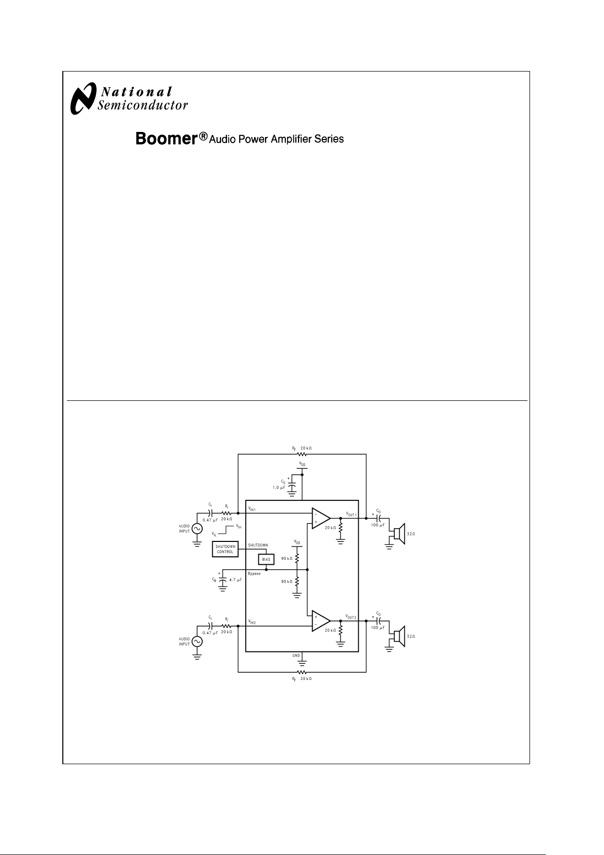
Typical Application
Boomer®is a registered trademark of National Semiconductor Corporation.
20008901
*Refer to the Application Information Section for information concerning proper selection of the input and output coupling capacitors.
FIGURE 1. Typical Audio Amplifier Application Circuit
November 2002
LM4810 Dual 105mW Headphone Amplifier with Active-High Shutdown Mode
© 2002 National Semiconductor Corporation DS200089 www.national.com
Page 2
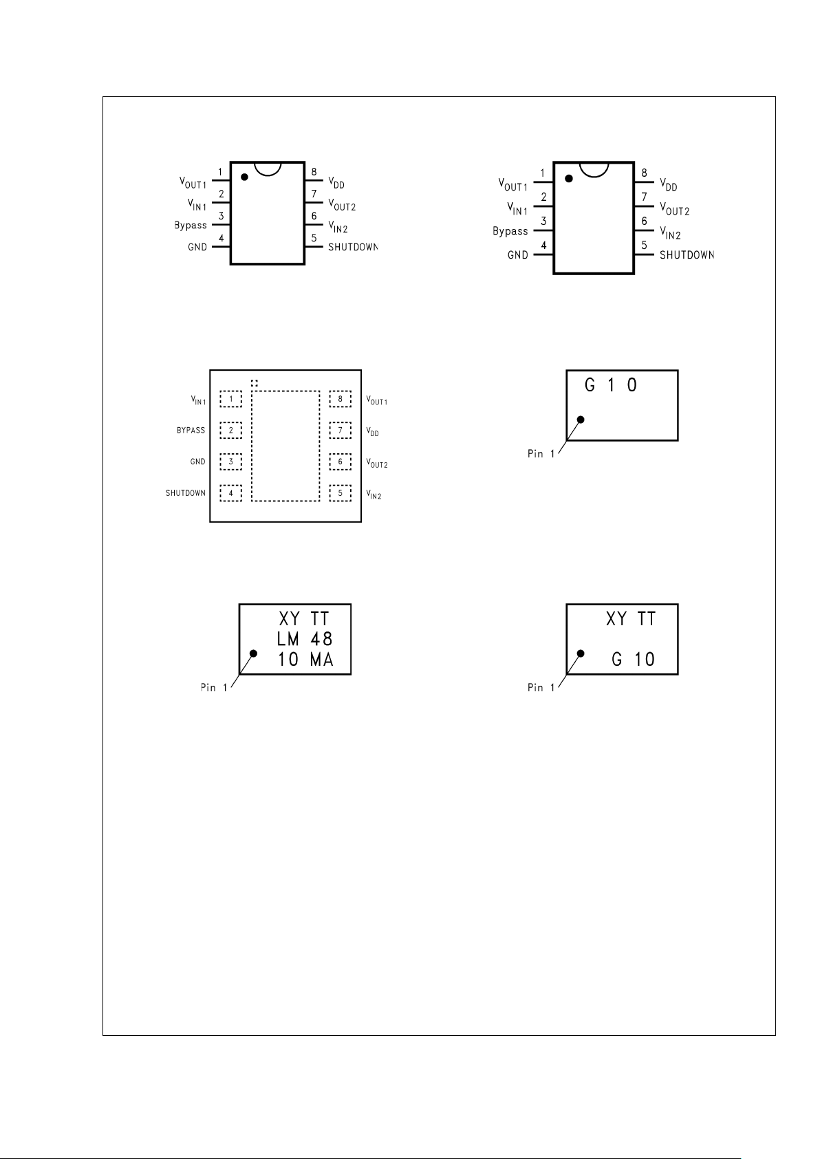
Connection Diagrams
MSOP Package SO Package
20008902
Top View
Order NumberLM4810MM
See NS Package Number MUA08A
20008902
Top View
Order NumberLM4810MA
See NS Package Number M08A
LLP Package MSOP Marking
20008986
Top View
Order NumberLM4810LD
See NS Package Number LDA08B
20008991
SO Marking LLP Marking
20008992 20008993
LM4810
www.national.com 2
Page 3
Absolute Maximum Ratings (Note 2)
If Military/Aerospace specified devices are required,
please contact the National Semiconductor Sales Office/
Distributors for availability and specifications.
Supply Voltage 6.0V
Storage Temperature −65˚C to +150˚C
ESD Susceptibility (Note 4) 3.5kV
ESD Machine Model (Note 8) 250V
Junction Temperature (T
J
) 150˚C
Soldering Information (Note 1)
Small Outline Package
Vapor Phase (60 sec.) 215˚C
Infrared (15 sec.) 220˚C
Thermal Resistance
θ
JA
(SO) 170˚C/W
θ
JC
(SO) 35˚C/W
θ
JA
(MSOP) 210˚C/W
θ
JC
(MSOP) 56˚C/W
θ
JA
(LLP) 117˚C/W (Note 9)
θ
JA
(LLP) 150˚C/W (Note 10)
θ
JC
(LLP) 15˚C/W
Operating Ratings (Note 2)
Temperature Range
T
MIN
≤ TA≤ T
MAX
−40˚C ≤ TA≤ 85˚C
Supply Voltage (V
CC
2.0V ≤ VCC≤ 5.5V
Note 1: See AN-450 “Surface Mounting and their Effects on Product Reliability” for other methods of soldering surface mount devices.
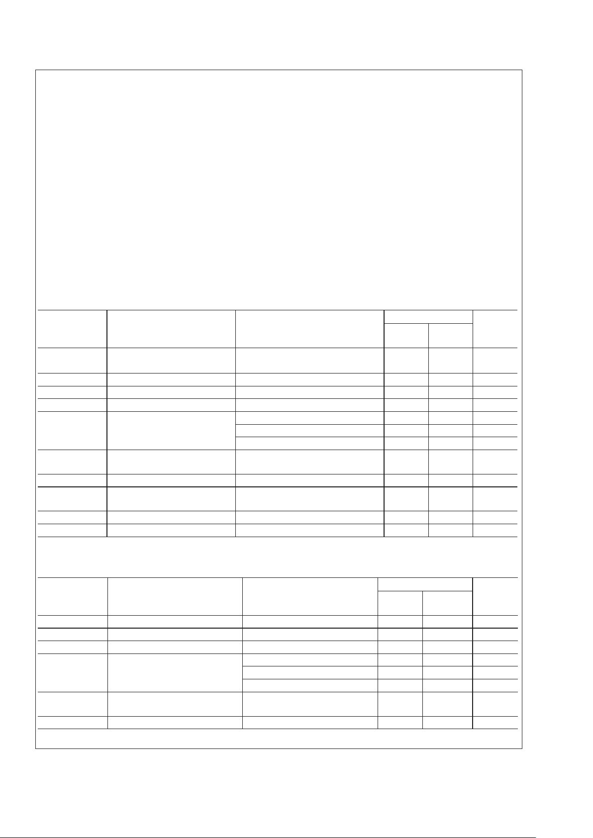
Electrical Characteristics (Notes 2, 3)
The following specifications apply for VDD= 5V unless otherwise specified, limits apply to TA= 25˚C.
Symbol Parameter Conditions LM4810 Units
(Limits)
Typ
(Note 5)
Limit
(Note 7)
V
DD
Supply Voltage 2.0 V (min)
5.5 V (max)
I
DD
Supply Current VIN= 0V, IO= 0A 1.3 3 mA(max)
I
SD
Shutdown Current VIN= 0V, V
SHUTDOWN
=V
DD
0.4 2 µA(max)
V
OS
Output Offset Voltage VIN= 0V 4.0 50 mV(max)
P
O
Output Power THD+N = 0.1%, f = 1kHz
R
L
=16Ω 105 mW
R
L
=32Ω 70 65 mW(min)
THD+N Total Harmonic Distortion P
O
= 50mW, RL=32Ω
f = 20Hz to 20kHz
0.3 %
Crosstalk Channel Separation R
L
=32Ω;PO= 70mW 70 dB
PSRR Power Supply Rejection Ratio C
B
= 1.0µF; V
RIPPLE
= 200mVPP,
f = 1kHz; Input terminated into 50Ω
70 dB
V
SDIH
Shutdown Voltage Input High 0.8 x V
DD
V (min)
V
SDIL
Shutdown Voltage Input Low 0.2 x V
DD
V (max)
Electrical Characteristics (Notes 2, 3)
The following specifications apply for VDD= 3.3V unless otherwise specified, limits apply to TA= 25˚C.
Symbol Parameter Conditions LM4810 Units
(Limits)
Typ
(Note 5)
Limit
(Note 7)
I
DD
Supply Current VIN= 0V, IO= 0A 1.0 mA
I
SD
Shutdown Current VIN= 0V, V
SHUTDOWN
=V
DD
0.4 µA
V
OS
Output Offset Voltage VIN= 0V 4.0 mV
P
O
Output Power THD+N = 0.1%, f = 1kHz
R
L
=16Ω 40 mW
R
L
=32Ω 28 mW
THD+N Total Harmonic Distortion P
O
= 25mW, RL=32Ω
f = 20Hz to 20kHz
0.4 %
Crosstalk Channel Separation RL=32Ω;PO= 25mW 70 dB
LM4810
www.national.com3
Page 4
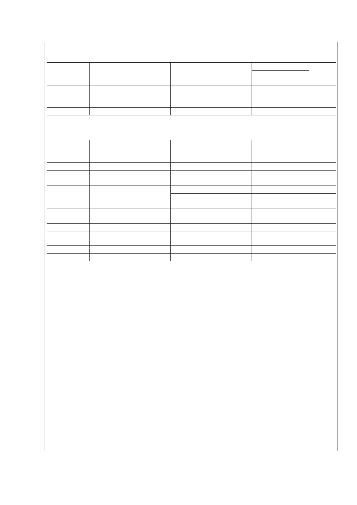
Electrical Characteristics (Notes 2, 3) (Continued)
The following specifications apply for VDD= 3.3V unless otherwise specified, limits apply to TA= 25˚C.
Symbol Parameter Conditions LM4810 Units
(Limits)
Typ
(Note 5)
Limit
(Note 7)
PSRR Power Supply Rejection Ratio C
B
= 1.0µF; Vripple = 200mVPP,
f = 1kHz; Input terminated into 50Ω
70 dB
V
SDIH
Shutdown Voltage Input High 0.8 x V
DD
V (min)
V
SDIL
Shutdown Voltage Input Low 0.2 x V
DD
V (max)
Electrical Characteristics (Notes 2, 3)
The following specifications apply for VDD= 2.6V unless otherwise specified, limits apply to TA= 25˚C.
Symbol Parameter Conditions LM4810 Units
(Limits)
Typ
(Note 5)
Limit
(Note 7)
I
DD
Supply Current VIN= 0V, IO= 0A 0.9 mA
I
SD
Shutdown Current VIN= 0V, V
SHUTDOWN
=V
DD
0.2 µA
V
OS
Output Offset Voltage VIN= 0V 4.0 mV
P
O
Output Power THD+N = 0.1%, f = 1kHz
R
L
=16Ω 20 mW
R
L
=32Ω 16 mW
THD+N Total Harmonic Distortion P
O
= 15mW, RL=32Ω
f = 20Hz to 20kHz
0.6 %
Crosstalk Channel Separation R
L
=32Ω;PO= 15mW 70 dB
PSRR Power Supply Rejection Ratio C
B
= 1.0µF; Vripple = 200mVPP,
f = 1kHz; Input terminated into 50Ω
70 dB
V
SDIH
Shutdown Voltage Input High 0.8 x V
DD
V (min)
V
SDIL
Shutdown Voltage Input Low 0.2 x V
DD
V (max)
Note 2: Absolute Maximum Ratings indicate limits beyond which damage to the device may occur.
Note 3: All voltages are measured with respect to the ground pin, unless otherwise specified.
Note 4: Human body model, 100pF discharged through a 1.5kΩ resistor.
Note 5: Typical specifications are specified at +25OC and represent the most likely parametric norm.
Note 6: Tested limits are guaranteed to National’s AOQL (Average Outgoing Quality Level).
Note 7: Datasheet max/min specification limits are guaranteed by design, test, or statistical analysis.
Note 8: Machine Model ESD test is covered by specification EIAJ IC-121-1981. A 200pF cap is charged to the specified voltage, then discharged directly into the
IC with no external series resistor (resistance of discharge path must be under 50Ohms).
Note 9: The given θ
JA
is for an LM4810 packaged in an LDA08B with the Exposed-Dap soldered to a printed circuit board copper pad with an area equivalent to
that of the Exposed-Dap itself.
Note 10: The given θ
JA
is for an LM4810 packaged in an LDA08B with the Exposed-Dap not soldered to any circuit board copper.
LM4810
www.national.com 4
Page 5
External Components Description (Figure 1)
Components Functional Description
1. R
i
The inverting input resistance, along with Rf, set the closed-loop gain. Ri, along with Ci, form a high
pass filter with f
c
= 1/(2πRiCi).
2. C
i
The input coupling capacitor blocks DC voltage at the amplifier’s input terminals. Ci, along with Ri,
create a highpass filter with f
c
= 1/(2πRiCi). Refer to the section, Selecting Proper External
Components, for an explanation of determining the value of C
i
.
3. R
f
The feedback resistance, along with Ri, set closed-loop gain.
4. C
S
This is the supply bypass capacitor. It provides power supply filtering. Refer to the Application
Information section for proper placement and selection of the supply bypass capacitor.
5. C
B
This is the BYPASS pin capacitor. It provides half-supply filtering. Refer to the section, Selecting
Proper External Components, for information concerning proper placement and selection of C
B
.
6. C
O
This is the output coupling capacitor. It blocks the DC voltage at the amplifier’s output and forms a high
pass filter with R
L
at fO= 1/(2πRLCO)
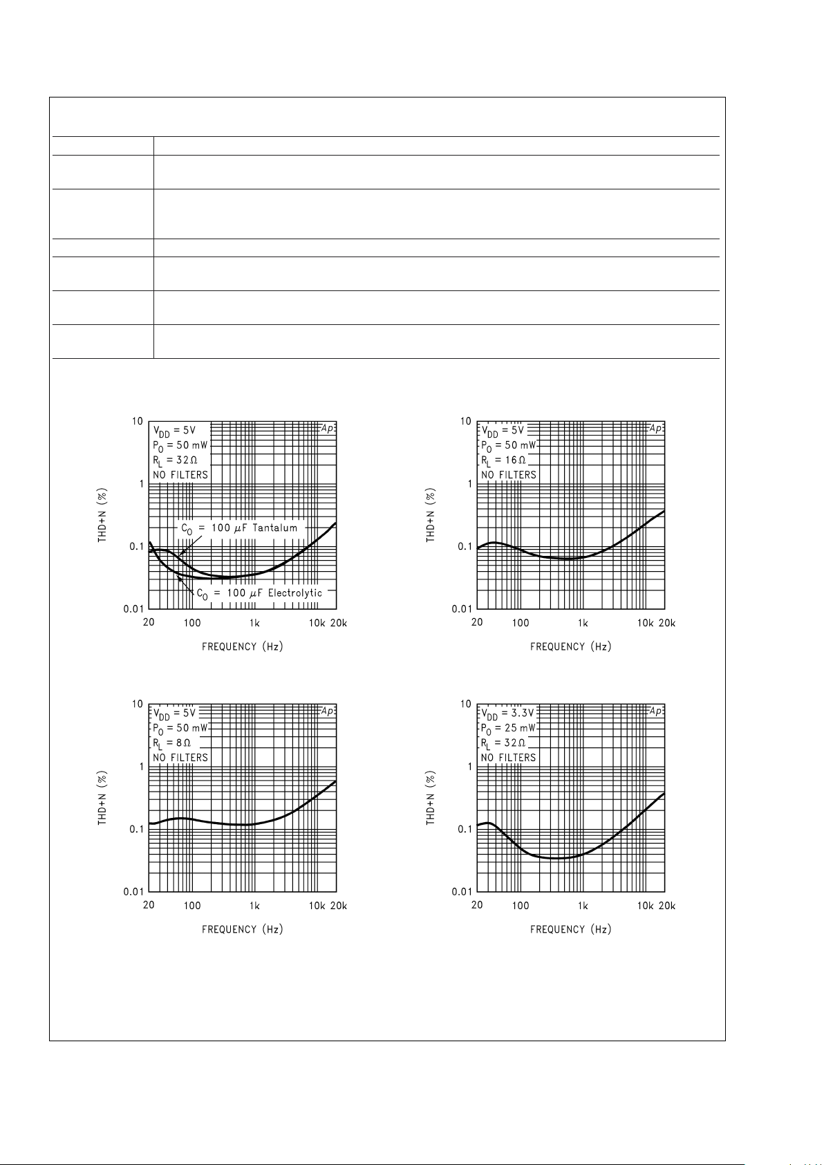
Typical Performance Characteristics
THD+N vs Frequency THD+N vs Frequency
20008985 20008964
THD+N vs Frequency THD+N vs Frequency
20008965 20008966
LM4810
www.national.com5
Page 6
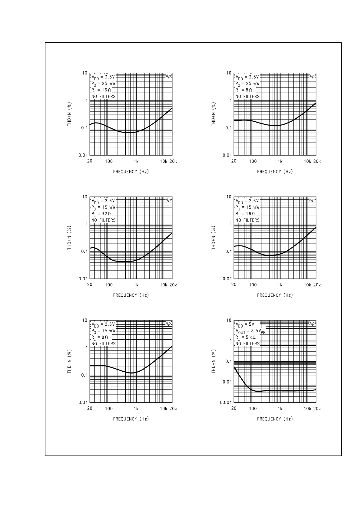
Typical Performance Characteristics (Continued)
THD+N vs Frequency THD+N vs Frequency
20008967 20008968
THD+N vs Frequency THD+N vs Frequency
20008969 20008970
THD+N vs Frequency THD+N vs Frequency
20008971 20008972
LM4810
www.national.com 6
Page 7

Typical Performance Characteristics (Continued)
THD+N vs Output Power THD+N vs Output Power
20008973 20008974
THD+N vs Output Power THD+N vs Output Power
20008975 20008976
THD+N vs Output Power THD+N vs Output Power
20008977 20008978
LM4810
www.national.com7
Page 8

Typical Performance Characteristics (Continued)
THD+N vs Output Power THD+N vs Output Power
20008979 20008980
THD+N vs Output Power
Output Power vs
Load Resistance
20008981
20008922
Output Power vs
Load Resistance
Output Power vs
Load Resistance
20008923 20008924
LM4810
www.national.com 8
Page 9

Typical Performance Characteristics (Continued)
Output Power vs
Supply Voltage
Output Power vs
Power Supply
20008925 20008926
Output Power vs
Power Supply
Dropout Voltage vs
Supply Voltage
20008927
20008984
Power Dissipation vs
Output Power
Power Dissipation vs
Output Power
20008929
20008930
LM4810
www.national.com9
Page 10

Typical Performance Characteristics (Continued)
Power Dissipation vs
Output Power
Channel Separation
20008931
20008982
Noise Floor Power Supply Rejection Ratio
20008934
20008983
Open Loop
Frequency Response
Open Loop
Frequency Response
20008950 20008951
LM4810
www.national.com 10
Page 11

Typical Performance Characteristics (Continued)
Open Loop
Frequency Response
Supply Current vs
Supply Voltage
20008938
20008944
Application Information
MICRO-POWER SHUTDOWN
The voltage applied to the SHUTDOWN pin controls the
LM4810’s shutdown function. Activate micro-power shutdown by applying a logic high voltage to the SHUTDOWN
pin. The logic threshold is typically V
DD
/2. When active, the
LM4810’s micro-power shutdown feature turns off the amplifier’s bias circuitry, reducing the supply current. The low
0.4µA typical shutdown current is achieved by applying a
voltage that is as near as V
DD
as possible to the SHUT-
DOWN pin. A voltage that is less than V
DD
may increase the
shutdown current.
There are a few ways to control the micro-power shutdown.
These include using a single-pole, single-throw switch, a
microprocessor, or a microcontroller. When using a switch,
connect an external 100kΩ pull-up resistor between the
SHUTDOWN pin and V
DD
. Connect the switch between the
SHUTDOWN pin and GND. Select normal amplifier operation by closing the switch. Opening the switch connects the
SHUTDOWN pin to V
DD
through the pull-up resistor, activating micro-power shutdown. The switch and resistor guarantee that the SHUTDOWN pin will not float. This prevents
unwanted state changes. In a system with a microprocessor
or a microcontroller, use a digital output to apply the control
voltage to the SHUTDOWN pin. Driving the SHUTDOWN pin
with active circuitry eliminates the pull-up resistor.
EXPOSED-DAP PACKAGE PCB MOUNTING
CONSIDERATION
The LM4810’s exposed-Dap (die attach paddle) package
(LD) provides a low thermal resistance between the die and
the PCB to which the part is mounted and soldered. This
allows rapid heat transfer from the die to the surrounding
PCB copper traces, ground plane, and surrounding air.
The LD package should have its DAP soldered to a copper
pad on the PCB. The DAP’s PCB copper pad may be connected to a large plane of continuous unbroken copper. This
plane forms a thermal mass, heat sink, and radiation area.
However, since the LM4810 is designed for headphone applications, connecting a copper plane to the DAP’s PCB
copper pad is not required. The LM4810’s Power Dissipation
vs Output Power Curve in the Typical Performance Char-
acteristics shows that the maximum power dissipated is just
45mW per amplifier with a 5V power supply and a 32Ω load.
Further detailed and specific information concerning PCB
layout, fabrication, and mounting an LD (LLP) package is
available from National Semiconductor’s Package Engineering Group under application note AN1187.
POWER DISSIPATION
Power dissipation is a major concern when using any power
amplifier and must be thoroughly understood to ensure a
successful design. Equation 1 states the maximum power
dissipation point for a single-ended amplifier operating at a
given supply voltage and driving a specified output load.
P
DMAX
=(VDD)2/(2π2RL) (1)
Since the LM4810 has two operational amplifiers in one
package, the maximum internal power dissipation point is
twice that of the number which results from Equation 1. Even
with the large internal power dissipation, the LM4810 does
not require heat sinking over a large range of ambient temperature. From Equation 1, assuming a 5V power supply and
a32Ω load, the maximum power dissipation point is 40mW
per amplifier. Thus the maximum package dissipation point
is 80mW. The maximum power dissipation point obtained
must not be greater than the power dissipation that results
from Equation 2:
P
DMAX
=(T
JMAX−TA
)/θ
JA
(2)
For package MUA08A, θ
JA
= 210˚C/W. T
JMAX
= 150˚C for
the LM4810. Depending on the ambient temperature, T
A
,of
the system surroundings, Equation 2 can be used to find the
maximum internal power dissipation supported by the IC
packaging. If the result of Equation 1 is greater than that of
Equation 2, then either the supply voltage must be de-
LM4810
www.national.com11
Page 12

Application Information (Continued)
creased, the load impedance increased or T
A
reduced. For
the typical application of a 5V power supply, with a 32Ω load,
the maximum ambient temperature possible without violating
the maximum junction temperature is approximately 133.2˚C
provided that device operation is around the maximum
power dissipation point. Power dissipation is a function of
output power and thus, if typical operation is not around the
maximum power dissipation point, the ambient temperature
may be increased accordingly. Refer to the Typical Perfor-
mance Characteristics curves for power dissipation information for lower output powers.
POWER SUPPLY BYPASSING
As with any power amplifier, proper supply bypassing is
critical for low noise performance and high power supply
rejection. Applications that employ a 5V regulator typically
use a 10µF in parallel with a 0.1µF filter capacitors to stabilize the regulator’s output, reduce noise on the supply line,
and improve the supply’s transient response. However, their
presence does not eliminate the need for a local 1.0µF
tantalum bypass capacitance connected between the
LM4810’s supply pins and ground. Keep the length of leads
and traces that connect capacitors between the LM4810’s
power supply pin and ground as short as possible. Connecting a 4.7µF capacitor, C
B
, between the BYPASS pin and
ground improves the internal bias voltage’s stability and
improves the amplifier’s PSRR. The PSRR improvements
increase as the bypass pin capacitor value increases. Too
large, however, increases the amplifier’s turn-on time. The
selection of bypass capacitor values, especially C
B
, depends
on desired PSRR requirements, click and pop performance
(as explained in the section, Selecting Proper External
Components), system cost, and size constraints.
SELECTING PROPER EXTERNAL COMPONENTS
Optimizing the LM4810’s performance requires properly selecting external components. Though the LM4810 operates
well when using external components with wide tolerances,
best performance is achieved by optimizing component values.
The LM4810 is unity-gain stable, giving a designer maximum
design flexibility. The gain should be set to no more than a
given application requires. This allows the amplifier to
achieve minimum THD+N and maximum signal-to-noise ratio. These parameters are compromised as the closed-loop
gain increases. However, low gain demands input signals
with greater voltage swings to achieve maximum output
power. Fortunately, many signal sources such as audio
CODECs have outputs of 1V
RMS
(2.83V
P-P
). Please refer to
the Audio Power Amplifier Design section for more information on selecting the proper gain.
Input and Output Capacitor Value Selection
Amplifying the lowest audio frequencies requires high value
input and output coupling capacitors (C
I
and COin Figure 1).
A high value capacitor can be expensive and may compromise space efficiency in portable designs. In many cases,
however, the speakers used in portable systems, whether
internal or external, have little ability to reproduce signals
below 150Hz. Applications using speakers with this limited
frequency response reap little improvement by using high
value input and output capacitors.
Besides affecting system cost and size, C
i
has an effect on
the LM4810’s click and pop performance. The magnitude of
the pop is directly proportional to the input capacitor’s size.
Thus, pops can be minimized by selecting an input capacitor
value that is no higher than necessary to meet the desired
−3dB frequency. Please refer to the Optimizing Click and
Pop Reduction Performance section for a more detailed
discussion on click and pop performance.
As shown in Figure 1, the input resistor, R
I
and the input
capacitor, C
I
, produce a −3dB high pass filter cutoff frequency that is found using Equation (3). In addition, the
output load R
L
, and the output capacitor CO, produce a -3db
high pass filter cutoff frequency defined by Equation (4).
f
I-3db
=1/2πRIC
I
(3)
f
O-3db
=1/2πRLC
O
(4)
Also, careful consideration must be taken in selecting a
certain type of capacitor to be used in the system. Different
types of capacitors (tantalum, electrolytic, ceramic) have
unique performance characteristics and may affect overall
system performance.
Bypass Capacitor Value Selection
Besides minimizing the input capacitor size, careful consideration should be paid to the value of C
B
, the capacitor
connected to the BYPASS pin. Since C
B
determines how
fast the LM4810 settles to quiescent operation, its value is
critical when minimizing turn-on pops. The slower the
LM4810’s outputs ramp to their quiescent DC voltage (nominally 1/2 V
DD
), the smaller the turn-on pop. Choosing C
B
equal to 4.7µF along with a small value of Ci(in the range of
0.1µF to 0.47µF), produces a click-less and pop-less shutdown function. As discussed above, choosing C
i
no larger
than necessary for the desired bandwith helps minimize
clicks and pops.
OPTIMIZING CLICK AND POP REDUCTION
PERFORMANCE
The LM4810 contains circuitry that minimizes turn-on and
shutdown transients or “clicks and pop”. For this discussion,
turn-on refers to either applying the power supply voltage or
when the shutdown mode is deactivated. During turn-on, the
LM4810’s internal amplifiers are configured as unity gain
buffers. An internal current source charges up the capacitor
on the BYPASS pin in a controlled, linear manner. The gain
of the internal amplifiers remains unity until the voltage on
the BYPASS pin reaches 1/2 V
DD
. As soon as the voltage on
the BYPASS pin is stable, the device becomes fully operational. During device turn-on, a transient (pop) is created
from a voltage difference between the input and output of the
amplifier as the voltage on the BYPASS pin reaches 1/2 V
DD
.
For this discussion, the input of the amplifier refers to the
node between R
I
and CI. Ideally, the input and output track
the voltage applied to the BYPASS pin. During turn-on, the
buffer-configured amplifier output charges the input capacitor, C
I
, through the input resistor, RI. This input resistor
delays the charging time of C
I
thereby causing the voltage
difference between the input and output that results in a
transient (pop). Higher value capacitors need more time to
reach a quiescent DC voltage (usually 1/2 V
DD
) when
charged with a fixed current. Decreasing the value of C
I
and
R
I
will minimize the turn-on pops at the expense of the
desired -3dB frequency.
Although the BYPASS pin current cannot be modified,
changing the size of C
B
alters the device’s turn-on time and
LM4810
www.national.com 12
Page 13

Application Information (Continued)
the magnitude of “clicks and pops”. Increasing the value of
C
B
reduces the magnitude of turn-on pops. However, this
presents a tradeoff: as the size of C
B
increases, the turn-on
time increases. There is a linear relationship between the
size of C
B
and the turn-on time. Here are some typical
turn-on times for various values of C
B
:
C
B
T
ON
0.1µF 80ms
0.22µF 170ms
0.33µF 270ms
0.47µF 370ms
0.68µF 490ms
1.0µF 920ms
2.2µF 1.8sec
3.3µF 2.8sec
4.7µF 3.4sec
10µF 7.7sec
In order eliminate “clicks and pops”, all capacitors must be
discharged before turn-on. Rapidly switching V
DD
may not
allow the capacitors to fully discharge, which may cause
“clicks and pops”. In a single-ended configuration, the output
is coupled to the load by C
O
. This capacitor usually has a
high value. C
O
discharges through internal 20kΩ resistors.
Depending on the size of C
O
, the discharge time constant
can be relatively large. To reduce transients in single-ended
mode, an external 1kΩ–5kΩ resistor can be placed in parallel with the internal 20kΩ resistor. The tradeoff for using
this resistor is increased quiescent current.
AUDIO POWER AMPLIFIER DESIGN
Design a Dual 70mW/32Ω Audio Amplifier
Given:
Power Output 70 mW
Load Impedance 32Ω
Input Level 1 Vrms (max)
Input Impedance 20kΩ
Bandwidth 100 Hz– 20 kHz
±
0.50dB
The design begins by specifying the minimum supply voltage
necessary to obtain the specified output power. One way to
find the minimum supply voltage is to use the Output Power
vs Supply Voltage curve in the Typical Performance Char-
acteristics section. Another way, using Equation (5), is to
calculate the peak output voltage necessary to achieve the
desired output power for a given load impedance. To account for the amplifier’s dropout voltage, two additional voltages, based on the Dropout Voltage vs Supply Voltage in the
Typical Performance Characteristics curves, must be
added to the result obtained by Equation (5). For a
single-ended application, the result is Equation (6).
(5)
V
DD
≥ (2V
OPEAK
+(V
OD
TOP
+V
OD
BOT
)) (6)
The Output Power vs Supply Voltage graph for a 32Ω load
indicates a minimum supply voltage of 4.8V. This is easily
met by the commonly used 5V supply voltage. The additional
voltage creates the benefit of headroom, allowing the
LM4810 to produce peak output power in excess of 70mW
without clipping or other audible distortion. The choice of
supply voltage must also not create a situation that violates
maximum power dissipation as explained above in the
Power Dissipation section. Remember that the maximum
power dissipation point from Equation (1) must be multiplied
by two since there are two independent amplifiers inside the
package. Once the power dissipation equations have been
addressed, the required gain can be determined from Equation (7).
(7)
Thus, a minimum gain of 1.497 allows the LM4810 to reach
full output swing and maintain low noise and THD+N perfromance. For this example, let A
V
=1.5.
The amplifiers overall gain is set using the input (R
i
) and
feedback (R
f
) resistors. With the desired input impedance
set at 20kΩ, the feedback resistor is found using Equation
(8).
A
V=Rf/Ri
(8)
The value of Rfis 30kΩ.
The last step in this design is setting the amplifier’s −3db
frequency bandwidth. To achieve the desired
±
0.25dB pass
band magnitude variation limit, the low frequency response
must extend to at lease one−fifth the lower bandwidth limit
and the high frequency response must extend to at least five
times the upper bandwidth limit. The gain variation for both
response limits is 0.17dB, well within the
±
0.25dB desired
limit. The results are an
f
L
= 100Hz/5 = 20Hz (9)
and a
fH= 20kHz*5 = 100kHz (10)
As stated in the External Components section, both R
i
in
conjunction with C
i
, and Cowith RL, create first order highpass filters. Thus to obtain the desired low frequency response of 100Hz within
±
0.5dB, both poles must be taken
into consideration. The combination of two single order filters
at the same frequency forms a second order response. This
results in a signal which is down 0.34dB at five times away
from the single order filter −3dB point. Thus, a frequency of
20Hz is used in the following equations to ensure that the
response is better than 0.5dB down at 100Hz.
C
i
≥ 1/(2π * 20kΩ * 20Hz) = 0.397µF; use 0.39µF. (11)
Co≥ 1/(2π *32Ω * 20Hz) = 249µF; use 330µF. (12)
The high frequency pole is determined by the product of the
desired high frequency pole, f
H
, and the closed-loop gain,
LM4810
www.national.com13
Page 14

Application Information (Continued)
A
V
. With a closed-loop gain of 1.5 and fH= 100kHz, the
resulting GBWP = 150kHz which is much smaller than the
LM4810’s GBWP of 900kHz. This figure displays that if a
designer has a need to design an amplifier with a higher
gain, the LM4810 can still be used without running into
bandwidth limitations.
Demonstration Board Schematic
20008959
FIGURE 2. LM4810 Demonstration Board Schematic
LM4810
www.national.com 14
Page 15

Demonstration Board Layout
20008960
FIGURE 3. Recommended PC Board Layout
Component-Side Silkscreen
20008961
FIGURE 4. Recommended PC Board Layout
Component-Side Layout
20008962
FIGURE 5. Recommended PC Board Layout
Bottom-Side Layout
LM4810
www.national.com15
Page 16

Demonstration Board Layout (Continued)
20008987
FIGURE 6. Recommended LD PC Board Layout
Component-Side Silkreen
20008988
FIGURE 7. Recommended LD PC Board Layout
Component-Side Layout
20008989
FIGURE 8. Recommended LD PC Board Layout
Bottom-Side Layout
LM4810
www.national.com 16
Page 17

Physical Dimensions inches (millimeters) unless otherwise noted
Order Number LM4810MM
NS Package Number MUA08A
Order Number LM4810MA
NS Package Number M08A
LM4810
www.national.com17
Page 18

Physical Dimensions inches (millimeters) unless otherwise noted (Continued)
Order Number LM4810LD
NS Package Number LDA08B
LIFE SUPPORT POLICY
NATIONAL’S PRODUCTS ARE NOT AUTHORIZED FOR USE AS CRITICAL COMPONENTS IN LIFE SUPPORT
DEVICES OR SYSTEMS WITHOUT THE EXPRESS WRITTEN APPROVAL OF THE PRESIDENT AND GENERAL
COUNSEL OF NATIONAL SEMICONDUCTOR CORPORATION. As used herein:
1. Life support devices or systems are devices or
systems which, (a) are intended for surgical implant
into the body, or (b) support or sustain life, and
whose failure to perform when properly used in
accordance with instructions for use provided in the
labeling, can be reasonably expected to result in a
significant injury to the user.
2. A critical component is any component of a life
support device or system whose failure to perform
can be reasonably expected to cause the failure of
the life support device or system, or to affect its
safety or effectiveness.
National Semiconductor
Corporation
Americas
Email: support@nsc.com
National Semiconductor
Europe
Fax: +49 (0) 180-530 85 86
Email: europe.support@nsc.com
Deutsch Tel: +49 (0) 69 9508 6208
English Tel: +44 (0) 870 24 0 2171
Français Tel: +33 (0) 1 41 91 8790
National Semiconductor
Asia Pacific Customer
Response Group
Tel: 65-2544466
Fax: 65-2504466
Email: ap.support@nsc.com
National Semiconductor
Japan Ltd.
Tel: 81-3-5639-7560
Fax: 81-3-5639-7507
www.national.com
LM4810 Dual 105mW Headphone Amplifier with Active-High Shutdown Mode
National does not assume any responsibility for use of any circuitry described, no circuit patent licenses are implied and National reserves the right at any time without notice to change said circuitry and specifications.
 Loading...