

Page 1
LM4755
Stereo 11W Audio Power Amplifier with Mute
n P
at 10%THD@1 kHz into 8Ω bridged TO-263 pkg.
General Description
The LM4755 is a stereo audio amplifier capable of delivering
11W per channel of continuous average output power to a
4Ω load or7Wperchannel into 8Ω using a single 24V supply
at 10%THD+N. The internal mute circuit and pre-set gain resistors provide for a very economical design solution.
Output power specifications at both 20V and 24V supplies
and low external component count offer high value to consumer electronic manufacturers for stereo TV and compact
stereo applications. The LM4755 is specifically designed for
single supply operation.
Key Specifications
n Output power at 10%THD with 1 kHz into 4Ω at VCC=
24V 11W(typ)
n Output power at 10%THD with 1 kHz into 8Ω at V
24V 7W(typ)
n Closed loop gain 34 dB(typ)
n P
at 10%THD@1 kHz into 4Ω single-ended TO-263
O
pkg. at V
=
12V 2.5W(typ)
CC
=
CC
O
=
at V
12V 5W(typ)
CC
Features
n Drives 4Ω and 8Ω loads
n Integrated mute function
n Internal Gain Resistors
n Minimal external components needed
n Single supply operation
n Internal current limiting and thermal protection
n Compact 9-lead TO-220 package
Applications
n Stereos TVs
n Compact stereos
n Mini component stereos
LM4755 Stereo 11W Audio Power Amplifier with Mute
February 1999
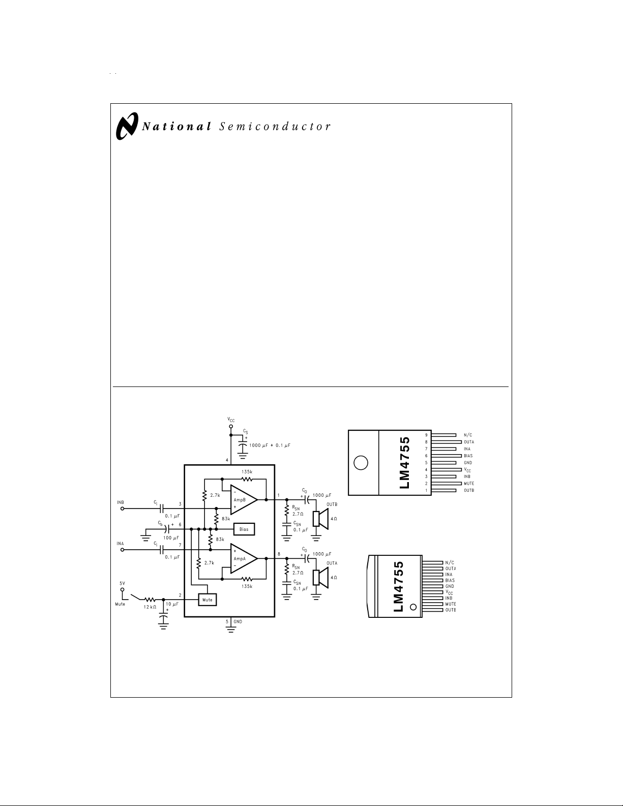
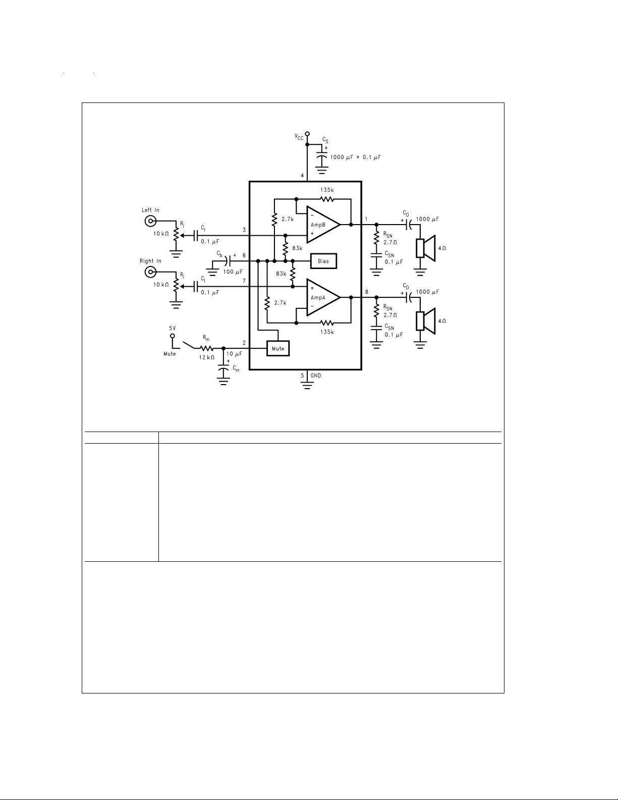
Typical Application Connection Diagrams
Plastic Package
Package Description
Top View
Order Number LM4755T
Package Number TA09A
DS100059-1
FIGURE 1. Typical Audio Amplifier Application Circuit
Top View
Order Number LM4755TS
Package Number TS9A
DS100059-2
DS100059-36
© 1999 National Semiconductor Corporation DS100059 www.national.com
Page 2
Absolute Maximum Ratings (Note 2)
If Military/Aerospace specified devices are required,
T Package (10 seconds) 250˚C
Storage Temperature −40˚C to 150˚C
please contact the National Semiconductor Sales Office/
Distributors for availability and specifications.
Supply Voltage 40V
Input Voltage
±
0.7V
Output Current Internally Limited
Power Dissipation (Note 3) 62.5W
ESD Susceptability (Note 4) 2 kV
Junction Temperature 150˚C
Operating Ratings
Temperature Range
T
≤ TA≤ T
MIN
MAX
Supply Voltage 9V to 32V
θ
JC
θ
JA
−40˚C ≤ TA≤ +85˚C
2˚C/W
76˚C/W
Soldering Information
Electrical Characteristics
The following specifications apply to each channel with VCC= 24V, TA= 25˚C unless otherwise specified.
Symbol Parameter Conditions
I
TOTAL
Total Quiescent Power
Supply Current
Mute Off 10 15 mA(max)
Typical
(Note 5)
Limit
7 mA(min)
Mute On 7 mA
LM4755
P
O
THD Total Harmonic Distortion f = 1 kHz, P
V
OSW
X
TALK
Output Power (Continuous
Average per Channel)
f = 1 kHz, THD+N = 10%,RL=8Ω 7W
f = 1 kHz, THD+N = 10%,R
V
= 20V, RL=8Ω 4W
S
V
= 20V, RL=4Ω 7W
S
f = 1 kHz, THD+N = 10%,R
= 12V, TO-263 Pkg.
V
S
= 1 W/ch, RL=8Ω 0.08
O
=4Ω 11 10 W(min)
L
=4Ω
L
2.5 W
Output Swing PO= 10W, RL=8Ω 15 V
P
= 10W, RL=4Ω 14 V
O
Channel Separation See Apps. Circuit 55 dB
f = 1 kHz, V
= 4 Vrms
O
PSRR Power Supply Rejection Ratio See Apps. Circuit 50 dB
f = 120 Hz, V
V
ODV
Differential DC Output Offset
Voltage
VIN= 0V 0.09 0.4 V(max)
= 1 mVrms
O
SR Slew Rate 2 V/µs
R
IN
PBW Power Bandwidth 3 dB BW at P
A
VCL
e
IN
I
O
Mute Pin
V
IL
V
IH
A
M
Note 1: All voltages are measured with respect to the GND pin (5), unless otherwse specified.
Note 2: Absolute Maximum Ratings indicate limits beyond which damage to the device may occur.Operating Ratings indicate conditions for which the device is func-
tional, but do not guarantee specific performance limits. Electrical Characteristics state DC and AC electrical specifications under particular test conditions which guarantee specific performance limits. This assumes that the device is within the Operating Ratings. Specifications are not guaranteed for parameters where no limit is
given, however, the typical value is a good indication of device performance.
Note 3: For operating at case temperatures above 25˚C, the device must be derated based on a 150˚C maximum junction temperature and a thermal resistance of
= 2˚C/W (junction to case). Refer to the section Determining the Maximum Power Dissipation in the Application Information section for more information.
θ
JC
Note 4: Human body model, 100 pF discharged through a 1.5 kΩ resistor.
Input Impedance 83 kΩ
= 2.5W, RL=8Ω 65 kHz
Closed Loop Gain
RL=8Ω 34 33 dB(min)
(Internally Set)
Noise IHF-A Weighting Filter, RL=8Ω
O
35 dB(max)
0.2 mVrms
Output Referred
Output Short Circuit Limit VIN= 0.5V, RL=2Ω 2 A(min)
Mute Low Input Voltage Not in Mute Mode 0.8 V(max)
Mute High Input Voltage In Mute Mode 2.0 2.5 V(min)
Mute Attenuation V
= 5.0V 80 dB
MUTE
Units
(Limits)
%
www.national.com 2
Page 3
Electrical Characteristics (Continued)
Note 5: Typicals are measured at 25˚C and represent the parametric norm.
Note 6: Limits are guaranteed that all parts are tested in production to meet the stated values.
Note 7: The TO-263 Package is not recommended for V
>
16V due to impractical heatsinking limitations.
S
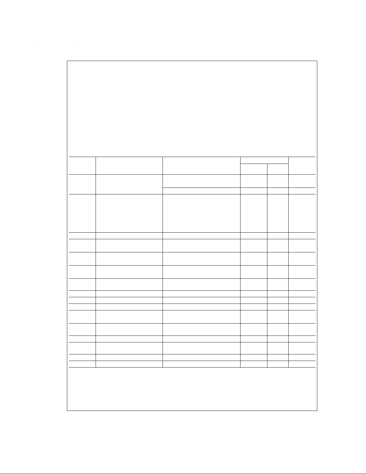
Equivalent Schematic
DS100059-3
www.national.com3
Page 4
Test Circuit
FIGURE 2. Test Circuit
www.national.com 4
DS100059-4
Page 5
System Application Circuit
FIGURE 3. Circuit for External Components Description
External Components Description
DS100059-5
Components Function Description
1, 2 C
3, 4 R
5, 6 C
7C
8, 9 C
10, 11 C
12, 13 R
14 R
15 C
Provides power supply filtering and bypassing.
S
Works with CSNto stabilize the output stage from high frequency oscillations.
SN
Works with RSNto stabilize the output stage from high frequency oscillations.
SN
Provides filtering for the internally generated half-supply bias generator.
b
Input AC coupling capacitor which blocks DC voltage at the amplifier’s input terminals. Also creates a
i
high pass filter with fc=1/(2
Output AC coupling capacitor which blocks DC voltage at the amplifier’s output terminal. Creates a high
o
pass filter with fc=1/(2
Voltage control - limits the voltage level allowed to the amplifier’s input terminals.
i
Works with Cmto provide mute function timing.
m
Works with Rmto provide mute function timing.
m
•π•
Rin•Cin).
•π•
Rout•Cout).
www.national.com5
Page 6
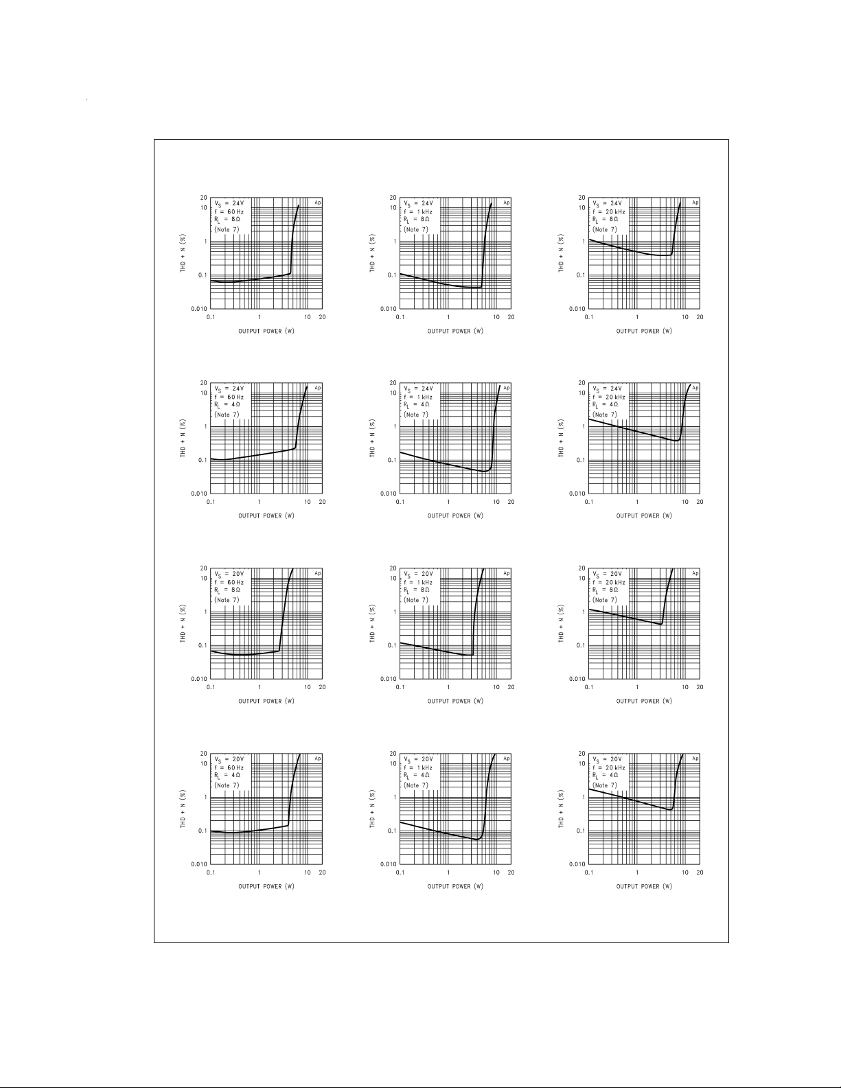
Typical Performance Characteristics(Note 5)
THD+N vs Output Power
THD+N vs Output Power
THD+N vs Output Power
DS100059-12
DS100059-6
THD+N vs Output Power
THD+N vs Output Power
THD+N vs Output Power
DS100059-13
DS100059-7
THD+N vs Output Power
DS100059-14
THD+N vs Output Power
DS100059-8
THD+N vs Output Power
DS100059-15
THD+N vs Output Power
DS100059-9
THD+N vs Output Power
www.national.com 6
DS100059-16
DS100059-10
DS100059-17
THD+N vs Output Power
DS100059-11
Page 7

Typical Performance Characteristics(Note 5) (Continued)
THD+N vs Output Power
THD+N vs Output Power
THD+N vs Output Power
DS100059-38
DS100059-41
THD+N vs Output Power
THD+N vs Output Power
THD+N vs Output Power
DS100059-39
DS100059-42
THD+N vs Output Power
DS100059-40
THD+N vs Output Power
DS100059-43
THD+N vs Output Power
THD+N vs Output Power
DS100059-44
DS100059-47
THD+N vs Output Power
DS100059-45
DS100059-48
DS100059-46
THD+N vs Output Power
DS100059-49
www.national.com7
Page 8

Typical Performance Characteristics(Note 5) (Continued)
Output Power vs Supply Voltage
DS100059-18
THD+N vs Frequency
DS100059-21
Channel Separation
Output Power vs Supply Voltage
DS100059-19
THD+N vs Frequency
DS100059-22
PSRR vs Frequency
Frequency Response
DS100059-20
Frequency Response
DS100059-23
Supply Current vs Supply Voltage
DS100059-24
Power Derating Curve
DS100059-27
Power Dissipation vs Output Power
www.national.com 8
DS100059-25
DS100059-28
DS100059-26
Power Dissipation vs Output Power
DS100059-29
Page 9

Typical Performance Characteristics(Note 5) (Continued)
Power Dissipation vs Output Power
DS100059-60
Power Dissipation vs Output Power
Application Information
The LM4755 contains circuitry to pull down the bias line internally, effectively shutting down the input stage. An external R-C should be used to adjust the timing of the pull-down.
If the bias line is pulled down too quickly, currents induced in
the internal bias resistors will cause a momentary DC voltage to appear across the inputs of each amplifier’s internal
differential pair, resulting in an output DC shift towards Vsupply. An R-C timing circuit should be used to limit the pulldown time such that output “pops” and signal feedthroughs
will be minimized. The pull-down timing is a function of a
number of factors, including the internal mute circuitry, the
voltage used to activate the mute, the bias capacitor, the
half-supply voltage, and internal resistances used in the halfsupply generator.
ues for the external R-C.
TABLE 1. Recommended Values for Mute Circuit
V
MUTE
5V 12V 18 kΩ 10 µF
5V 15V 18 kΩ 10 µF
5V 20V 12 kΩ 10 µF
5V 24V 12 kΩ 10 µF
5V 28V 8.2 kΩ 10 µF
5V 30V 8.2 kΩ 10 µF
Table 1
shows a list of recommended val-
V
CC
Rm Cm
DS100059-61
earlier in the External Components section these capacitors create high-pass filters with their corresponding input/
output impedances. The TypicalApplication Circuit shown
in
Figure 1
shows input and output capacitors of 0.1 µF and
1,000 µF respectively. At the input, with an 83 kΩ typical input resistance, the result is a high pass 3 dB point occurring
at 19 Hz. There is another high pass filter at 39.8 Hz created
with the output load resistance of 4Ω. Careful selection of
these components is necessary to ensure that the desired
frequency response is obtained. The Frequency Response
curves in the Typical Performance Characteristics section
show how different output coupling capacitors affect the low
frequency roll-off.
OPERATING IN BRIDGE-MODE
Though designed for use as a single-ended amplifier, the
LM4755 can be used to drive a load differentially (bridgemode). Due to the low pin count of the package, only the
non-inverting inputs are available. An inverted signal must
be provided to one of the inputs. This can easily be done with
the use of an inexpensive op-amp configured as a standard
inverting amplifier.An LF353 is a good low-cost choice. Care
must be taken, however, for a bridge-mode amplifier must
theoretically dissipate four times the power of a single-ended
type. The load seen by each amplifier is effectively half that
of the actual load being used, thus an amplifier designed to
drive a 4Ω load in single-ended mode should drive an 8Ω
load when operating in bridge-mode.
CAPACITOR SELECTION AND FREQUENCY
RESPONSE
With the LM4755, as in all single supply amplifiers, AC coupling capacitors are used to isolate the DC voltage present at
the inputs (pins 3, 7) and outputs (pins 1, 8). As mentioned
www.national.com9
Page 10

Application Information (Continued)
FIGURE 4. Bridge-Mode Application
DS100059-30
DS100059-31
FIGURE 5. THD+N vs P
OUT
PREVENTING OSCILLATIONS
With the integration of the feedback and bias resistors onchip, the LM4755 fits into a very compact package. However,
due to the close proximity of the non-inverting input pins to
the corresponding output pins, the inputs should be AC terminated at all times. If the inputs are left floating, the amplifier will have a positive feedback path through high impedance coupling, resulting in a high frequency oscillation. In
most applications, this termination is typically provided by
the previous stage’s source impedance. If the application will
www.national.com 10
DS100059-37
for Bridge-Mode Application
require an external signal, the inputs should be terminated to
ground with a resistance of 50 kΩ or less on the AC side of
the input coupling capacitors.
UNDERVOLTAGE SHUTDOWN
If the power supply voltage drops below the minimum operating supply voltage, the internal under-voltage detection circuitry pulls down the half-supply bias line, shutting down the
preamp section of the LM4755. Due to the wide operating
supply range of the LM4755, the threshold is set to just under 9V. There may be certain applications where a higher
Page 11

Application Information (Continued)
threshold voltage is desired. One example is a design requiring a high operating supply voltage, with large supply and
bias capacitors, and there is little or no other circuitry connected to the main power supply rail. In this circuit, when the
power is disconnected, the supply and bias capacitors will
discharge at a slower rate, possibly resulting in audible output distortion as the decaying voltage begins to clip the output signal. An external circuit may be used to sense for the
desired threshold, and pull the bias line (pin 6) to ground to
disable the input preamp.
such a circuit. When the voltage across the zener diode
drops below its threshold, current flow into the base of Q1 is
interrupted. Q2 then turns on, discharging the bias capacitor.
This discharge rate is governed by several factors, including
the bias capacitor value, the bias voltage, and the resistor at
the emitter of Q2.An equation for approximating the value of
the emitter discharge resistor, R, is given below:
R = (0.7v) / (Cb
Note that this is only a linearized approximation based on a
discharge time of 0.1s. The circuit should be evaluated and
adjusted for each application.
As mentioned earlier in the Built-in Mute Circuit section,
when using an external circuit to pull down the bias line, the
rate of discharge will have an effect on the turn-off induced
distortions. Please refer to the Built-in Mute Circuit section
for more information.
FIGURE 6. External Undervoltage Pull-Down
THERMAL CONSIDERATIONS
Heat Sinking
Proper heatsinking is necessary to ensure that the amplifier
will function correctly under all operating conditions. A heatsink that is too small will cause the die to heat excessively
and will result in a degraded output signal as the thermal protection circuitry begins to operate.
The choice of a heatsink for a given application is dictated by
several factors: the maximum power the IC needs to dissipate, the worst-case ambient temperature of the circuit, the
junction-to-case thermal resistance, and the maximum junction temperature of the IC. The heat flow approximation
equation used in determining the correct heatsink maximum
thermal resistance is given below:
T
J–TA=PDMAX
•
where:
Figure 6
(VCC/2) / 0.1s)
•
(θJC+ θCS+ θSA)
shows an example of
DS100059-32
P
= maximum power dissipation of the IC
DMAX
(˚C) = junction temperature of the IC
T
J
(˚C) = ambient temperature
T
A
(˚C/W) = junction-to-case thermal resistance of the IC
θ
JC
(˚C/W) = case-to-heatsink thermal resistance (typically
θ
CS
0.2 to 0.5 ˚C/W)
θ
(˚C/W) = thermal resistance of heatsink
SA
When determining the proper heatsink, the above equation
should be re-written as:
θ
≤ [(TJ–TA)/P
SA
DMAX
]-θJC–θ
CS
TO-263 HEATSINKING
Surface mount applications will be limited by the thermal dissipation properties of printed circuit board area. The TO-263
package is not recommended for surface mount applications
>
with V
There are TO-263 package enhancements, such as clip-on
16V due to limited printed circuit board area.
S
heatsinks and heatsinks with adhesives, that can be used to
improve performance.
Standard FR-4 single-sided copper clad will have an approximate Thermal resistance (θ
1.5 x 1.5 in. sq. 20–27˚C/W (T
2 x 2 in. sq. 16–23˚C/W
The above values for θ
proportions (i.e. variations in width and length will vary θ
SA
) ranging from:
SA
=28˚C, Sine wave
A
testing, 1 oz. Copper)
vary widely due to dimensional
SA
For audio applications, where peak power levels are short in
duration, this part will perform satisfactory with less
heatsinking/copper clad area. As with any high power design
proper bench testing should be undertaken to assure the design can dissipate the required power. Proper bench testing
requires attention to worst case ambient temperature and air
flow.At high power dissipation levels the part will show a tendency to increase saturation voltages, thus limiting the undistorted power levels.
DETERMINING MAXIMUM POWER DISSIPATION
For a single-ended class AB power amplifier, the theoretical
maximum power dissipation point is a function of the supply
voltage, V
following equation:
(single channel)
P
DMAX
, and the load resistance, RLand is given by the
S
2
(W)=[V
2
S
/(2•π
RL)]
•
The above equation is for a single channel class-AB power
amplifier. For dual amplifiers such as the LM4755, the equation for calculating the total maximum power dissipated is:
(dual channel)
P
(W)=2•[V
DMAX
or
2
2
/(π
V
S
RL)
•
(Bridged Outputs)
(W) = 4[V
P
DMAX
S
S
2
/(2π
2
/(2•π
2
RL)]
•
2
RL)]
•
HEATSINK DESIGN EXAMPLE:
Determine the system parameters:
= 24V Operating Supply Voltage
V
S
R
=4Ω Minimum Load Impedance
L
T
= 55˚C Worst Case Ambient Temperature
A
Device parameters from the datasheet:
T
= 150˚C Maximum Junction Temperature
J
).
www.national.com11
Page 12

Application Information (Continued)
θ
= 2˚C/W Junction-to-Case Thermal Resistance
JC
Calculations:
2
P
=2•[V
•
DMAX
= 14.6W
θ
≤ [(TJ-TA)/P
SA
- 2˚C/W–0.2˚C/W = 4.3˚C/W
DMAX
Conclusion: Choose a heatsink with θ
TO-263 HEATSINK DESIGN EXAMPLES:
Example 1: (Stereo Single-Ended Output)
=
T
R
V
θ
DMAX
=
A
=
J
L
S
JC
V
30˚C
150˚C
=
4Ω
=
12V
=
2˚C/W
CC
Given: T
from PDvs POGraph:
P
DMAX
Calculating P
P
DMAX
Calculating Heatsink Thermal Resistance:
<
θ
SA
<
θ
120˚C/3.7W − 2.0˚C/W − 0.2˚C/W=30.2˚C/W
SA
Therefore the recommendation is to use 1.5 x 1.5 square
inch of single-sided copper clad.
Example 2: (Stereo Single-Ended Output)
Given: T
P
DMAX
=
50˚C
A
=
150˚C
T
J
=
4Ω
R
L
=
12V
V
S
=
2˚C/W
θ
JC
from PDvs POGraph:
2
2
S
/2•π
RL)] = (24V)2/(2•π
•
]-θJC–θCS= [ (150˚C - 55˚C) / 14.6W]
≤ 4.3˚C/W.
SA
≈ 3.7W
P
DMAX
:
2
/(π2RL)=(12V)2/π2(4Ω))=3.65W
TJ−TA/P
DMAX
− θJC− θ
CS
2
4Ω)
•
P
≈ 3.7W
DMAX
Calculating P
P
DMAX
:
DMAX
2
=
/(π2RL)=(12V)2/(π2(4Ω))=3.65W
V
CC
Calculating Heatsink Thermal Resistance:
<
[(TJ−TA)/P
θ
SA
<
θ
100˚C/3.7W − 2.0˚C/W − 0.2˚C/W=24.8˚C/W
SA
DMAX
]−θJC− θ
CS
Therefore the recommendation is to use 2.0 x 2.0 square
inch of single-sided copper clad.
Example 3: (Bridged Output)
Given: T
Calculating P
P
DMAX
=
50˚C
A
=
150˚C
T
J
=
8Ω
R
L
=
12V
V
S
=
2˚C/W
θ
JC
:
DMAX
2
=
/(2π2RL)]=4(12V)2/(2π2(8Ω))=3.65W
4[V
CC
Calculating Heatsink Thermal Resistance:
<
[(TJ−TA)/P
θ
SA
<
θ
100˚C / 3.7W − 2.0˚C/W − 0.2˚C/W=24.8˚C/W
SA
DMAX
]−θJC− θ
CS
Therefore the recommendation is to use 2.0 x 2.0 square
inch of single-sided copper clad.
LAYOUT AND GROUND RETURNS
Proper PC board layout is essential for good circuit performance. When laying out a PC board for an audio power amplifier, particular attention must be paid to the routing of the
output signal ground returns relative to the input signal and
bias capacitor grounds. To prevent any ground loops, the
ground returns for the output signals should be routed separately and brought together at the supply ground. The input
signal grounds and the bias capacitor ground line should
also be routed separately. The 0.1 µF high frequency supply
bypass capacitor should be placed as close as possible to
the IC.
www.national.com 12
Page 13

Application Information (Continued)
PC BOARD LAYOUT-COMPOSITE
DS100059-33
www.national.com13
Page 14

Application Information (Continued)
PC BOARD LAYOUT-SILK SCREEN
www.national.com 14
DS100059-34
Page 15

Application Information (Continued)
PC BOARD LAYOUT-SOLDER SIDE
DS100059-35
www.national.com15
Page 16

16
Page 17

Physical Dimensions inches (millimeters) unless otherwise noted
Order Number LM4755T
NS Package Number TA9A
www.national.com17
Page 18

Physical Dimensions inches (millimeters) unless otherwise noted (Continued)
Order Number LM4755TS
NS Package Number TS9A
LM4755 Stereo 11W Audio Power Amplifier with Mute
LIFE SUPPORT POLICY
NATIONAL’S PRODUCTS ARE NOT AUTHORIZED FOR USE AS CRITICAL COMPONENTS IN LIFE SUPPORT DEVICES OR SYSTEMS WITHOUT THE EXPRESS WRITTEN APPROVAL OF THE PRESIDENT OF NATIONAL SEMICONDUCTOR CORPORATION. As used herein:
1. Life support devices or systems are devices or systems which, (a) are intended for surgical implant into
the body, or (b) support or sustain life, and whose failure to perform when properly used in accordance
with instructions for use provided in the labeling, can
be reasonably expected to result in a significant injury
to the user.
National Semiconductor
Corporation
Americas
Tel: 1-800-272-9959
Fax: 1-800-737-7018
Email: support@nsc.com
www.national.com
National does not assume any responsibility for use of any circuitry described, no circuit patent licenses are implied and National reserves the right at any time without notice to change said circuitry and specifications.
National Semiconductor
Europe
Fax: +49 (0) 1 80-530 85 86
Email: europe.support@nsc.com
Deutsch Tel: +49 (0) 1 80-530 85 85
English Tel: +49 (0) 1 80-532 78 32
Français Tel: +49 (0) 1 80-532 93 58
Italiano Tel: +49 (0) 1 80-534 16 80
2. A critical component is any component of a life support
device or system whose failure to perform can be reasonably expected to cause the failure of the life support
device or system, or to affect its safety or effectiveness.
National Semiconductor
Asia Pacific Customer
Response Group
Tel: 65-2544466
Fax: 65-2504466
Email: sea.support@nsc.com
National Semiconductor
Japan Ltd.
Tel: 81-3-5639-7560
Fax: 81-3-5639-7507
 Loading...