

Page 1
LM4753
Dual 10W Audio Power Amplifier w/Mute, Standby and
Volume Control
General Description
The LM4753 is a stereo audio amplifier capable of delivering
10W/channel at 10%distortion into a 8Ω load. The power
amp has an internally set gain of 30 dB. A 0V–5V DC controlled volume block provides80dBofattenuationfrom input
to line-out. Line outputs are available after the volume control for signal routing.
The amplifier has a smooth transition fade-in/out mute and a
power conserving standby function which are controlled
through TTL or CMOS logic. Both functions provide over
75 dB of attenuation.
The LM4753 maintains an excellent Signal-to-Noise ratio of
greater than 70 dB with a low noise floor less than 2 mV.The
IC also maintains above 50 dB of channel separation.
The LM4753 is available in a 15-lead non-isolated plastic
package and is designed for use in TV applications requiring
single supply operation.
Key Specifications
n Output power into 8Ω at 10%THD 10W
n Maximum operating voltage 28V
n Power output stage Noise floor 2 mV
n Line output Noise floor 55 µV
n 0V–5V DC controlled volume attenuation 80 dB
n Mute attenuation 75 dB
n Standby-mode supply current 7 mA
Features
n Quiet fade-in/out mute function
n Stereo variable line-out pins
n AC output short circuit protection
n Thermal shutdown protection
Applications
n Stereo TVs
n Component stereo
n Compact stereo
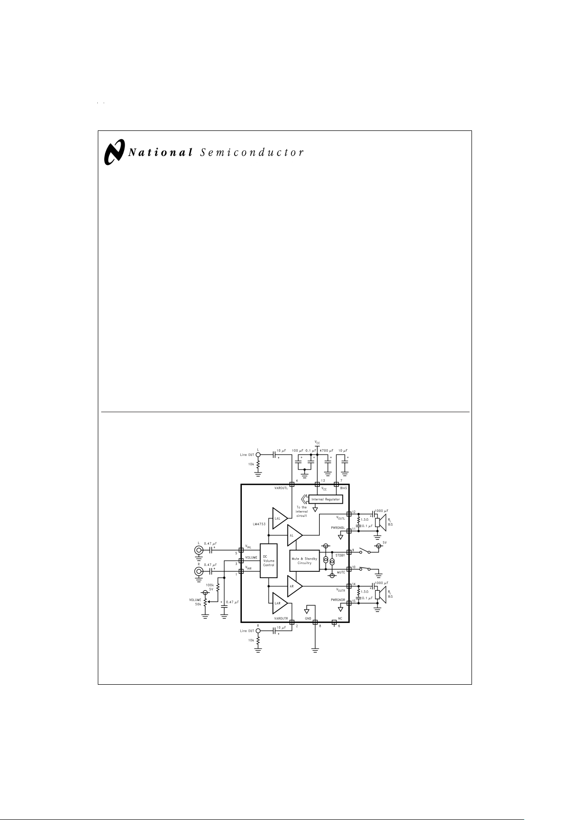
Typical Application
DS100043-1
FIGURE 1. Typical Audio Amplifier Application Circuit
June 1999
LM4753 Dual 10W Audio Power Amplifier w/Mute, Standby and Volume Control
© 1999 National Semiconductor Corporation DS100043 www.national.com
Page 2
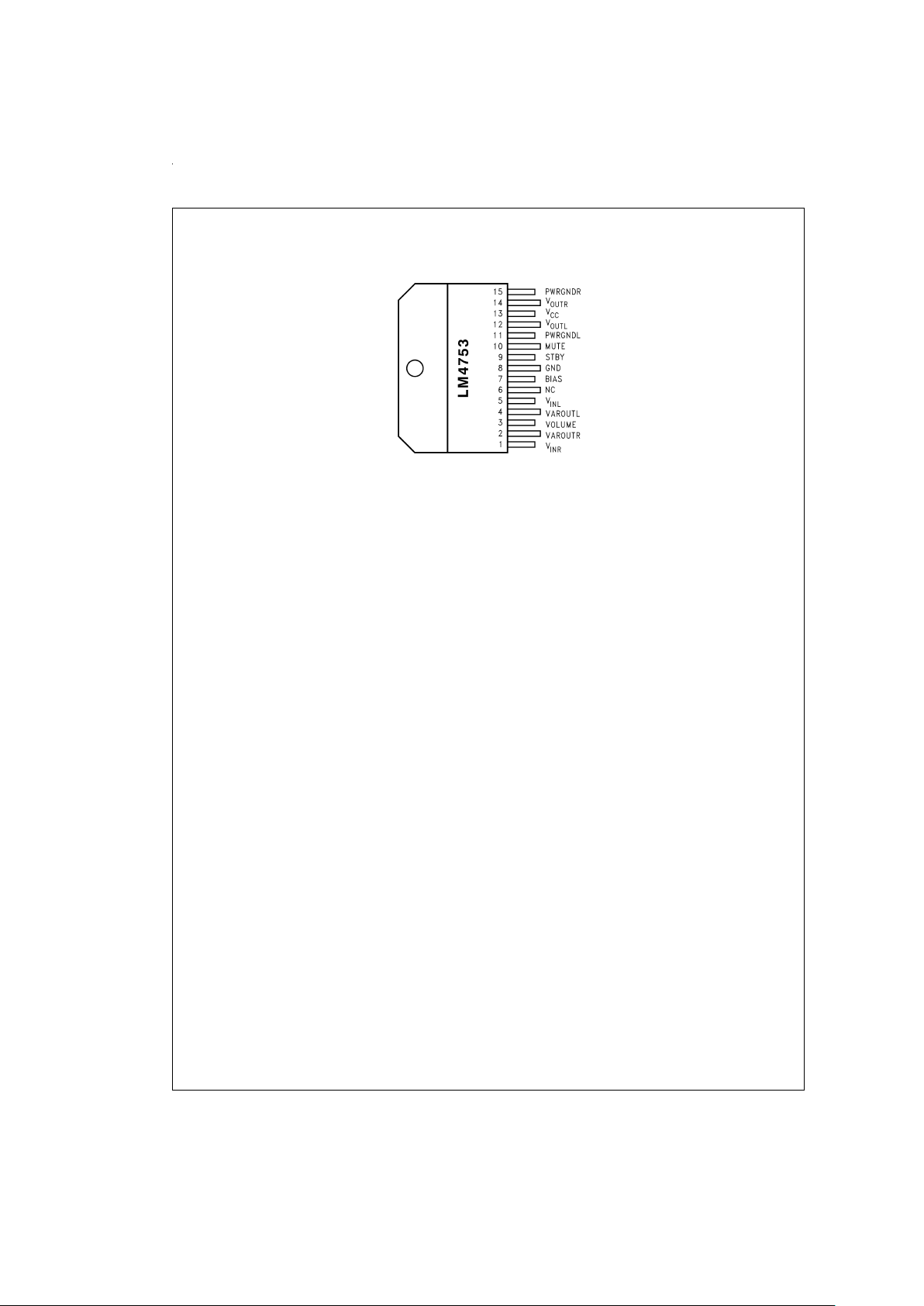
Connection Diagram
Plastic Package
DS100043-2
Top View
Order Number
See NS Package Number TA15A for
Staggered Lead Non-Isolated Package
www.national.com 2
Page 3
Absolute Maximum Ratings (Notes 3, 4)
If Military/Aerospace specified devices are required,
please contact the National Semiconductor Sales Office/
Distributors for availability and specifications.
Supply Voltage 32V
Output Current Internally Limited
Power Dissipation (Note 5) 22W
ESD Susceptibility (Note 6) 2000V
ESD Susceptibility (Note 7) 250V
Junction Temperature 150˚C
Soldering Information
T Package (10 sec) 260˚C
Storage Temperature −40˚C to +150˚C
Input Signal Voltage Range
±
3V
Operating Ratings (Notes 3, 4)
Temperature Range
T
MIN
≤ TA≤ T
MAX
−40˚C ≤ TA≤ +85˚C
Supply Voltage 15V to 28V
θ
JA
(Junction to Ambient) 35˚C/W
θ
JC
(Junction to Case) 1.5˚C/W
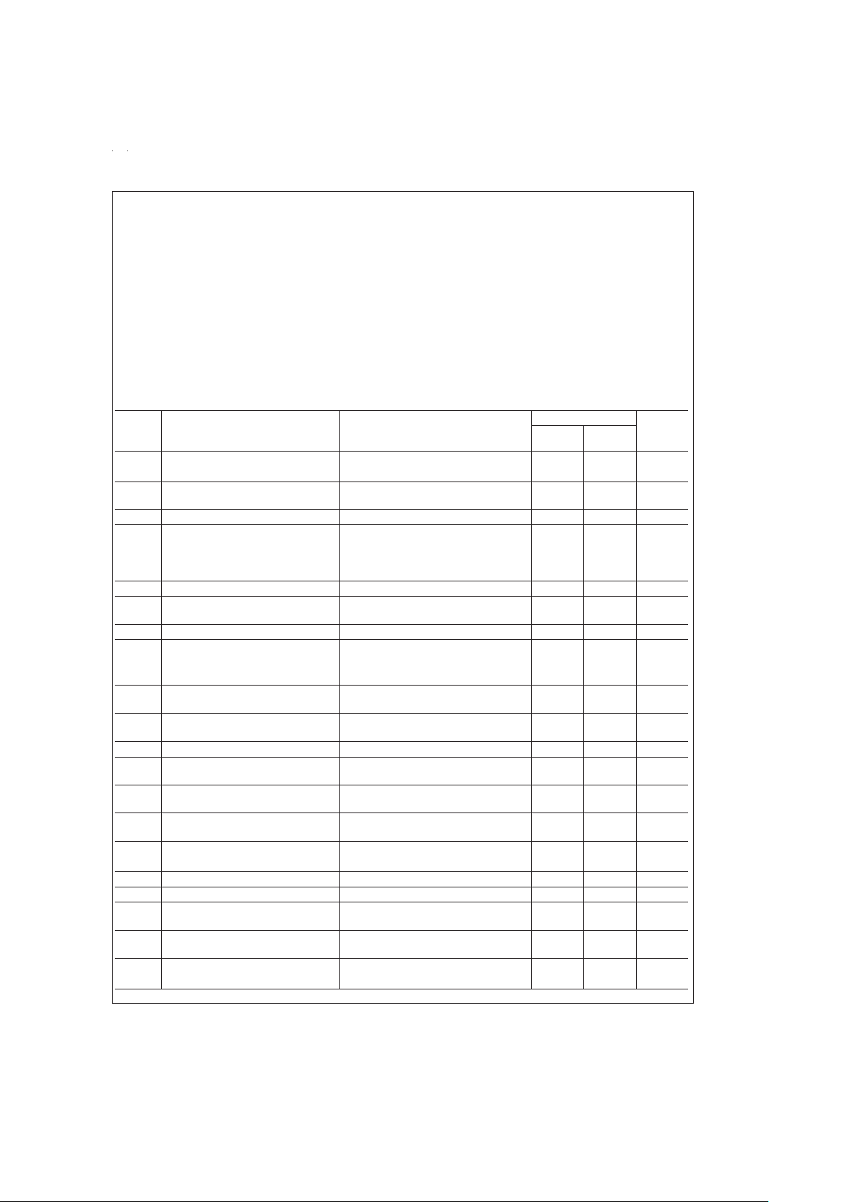
Electrical Characteristics (Notes 3, 4)
The following specifications apply for VCC= +22V, and Volume@0 dB unless otherwise specified. Limits apply for TA= 25˚C.
Symbol Parameter Conditions
LM4753
Units
(Limits)
Typical
(Note 8)
Limit
(Note 9)
I
CQ
(Note 1)
Total Quiescent Power Supply
Current
V
CM
= 0V, Vo= 0V, Io= 0 mA 20 mA (min)
80 140 mA (max)
I
STBY
(Note 1)
Standby Current V
STDBY
= 5V, Standby-on 7 10 mA (max)
I
MUTE
Mute Current V
MUTE
= 5V Mute-on 13 20 mA
A
M
(Note 2)
Mute Attenuation V
MUTE
= 5V, V
STDBY
= 0V. Mute-on
Signal Input
75 60 dB (min)
V
MUTE
= 0V. V
STDBY
= 0V. Mute-off
2 Vrms
±
5dB
Volume Attenuation Range 80 70 dB (min)
Volume Absolute Attenuation
Line-out
Pin 3
@
0V=80 dB, 2V=14 dB,
3V=8 dB, 4V=3 dB, 5V=0dB
±
3
±
5 dB (max)
Line-out Offset Voltage 20 40 mV (max)
P
O
(Note 1)
Output Power (Continuous Average) THD+N = 10%(max)
f = 1 kHz, R
L
=8Ω,VCC= 28 11.8 W
f = 1 kHz, R
L
=8Ω,VCC= 22V 7 6.5 W(min)
THD+N
(Note 2)
Total Harmonic Distortion Plus Noise P
o
=1W,f=1kHz, RL=8Ω 0.4 1
%
(max)
Xtalk
(Note 2)
Channel Separation f = 1 kHz, P
o
= 5W, RL=8Ω 50 dB
Power Amp Closed-Loop Gain Error Internal Gain = 30 dB 0.5
±
1 dB (max)
SR
(Note 2)
Slew Rate V
IN
= 100 mVp-p, t
RISE
= 2 ns, RL=8Ω 3 V/µs
R
IN
(Note 1)
Input Impedance 32 kΩ
I
O
(Note 1)
Output Current Limit V
IN
= 100 mV DC, tON= 1 ms, RL=1Ω 2.5 2.0 A(min)
PSRR
(Note 2)
Power Supply Rejection Ratio Vpin 13 AC = 1 Vrms, f = 100 Hz 50 dB
V
CM
= 0V, Io=0mA
GBWP Gain-Bandwidth Product f
o
= 100 kHz, VIN= 50 mvrms 2 MHz
Power Bandwidth −3 dB Bandwidth at 5W 90 kHz
eVCA
out
VCA Output Noise IHF - A Weighting Filter
R
IN
=25Ω
55 µV
e
out
Power Amp Output Noise IHF - A Weighting Filter
R
IN
=25Ω
1.8 mV
SNR Signal-to-Noise Ratio Measured at 1 kHz, R
s
=25Ω
P
o
= 4.8W, A - Weighted, 70 dB
www.national.com3
Page 4
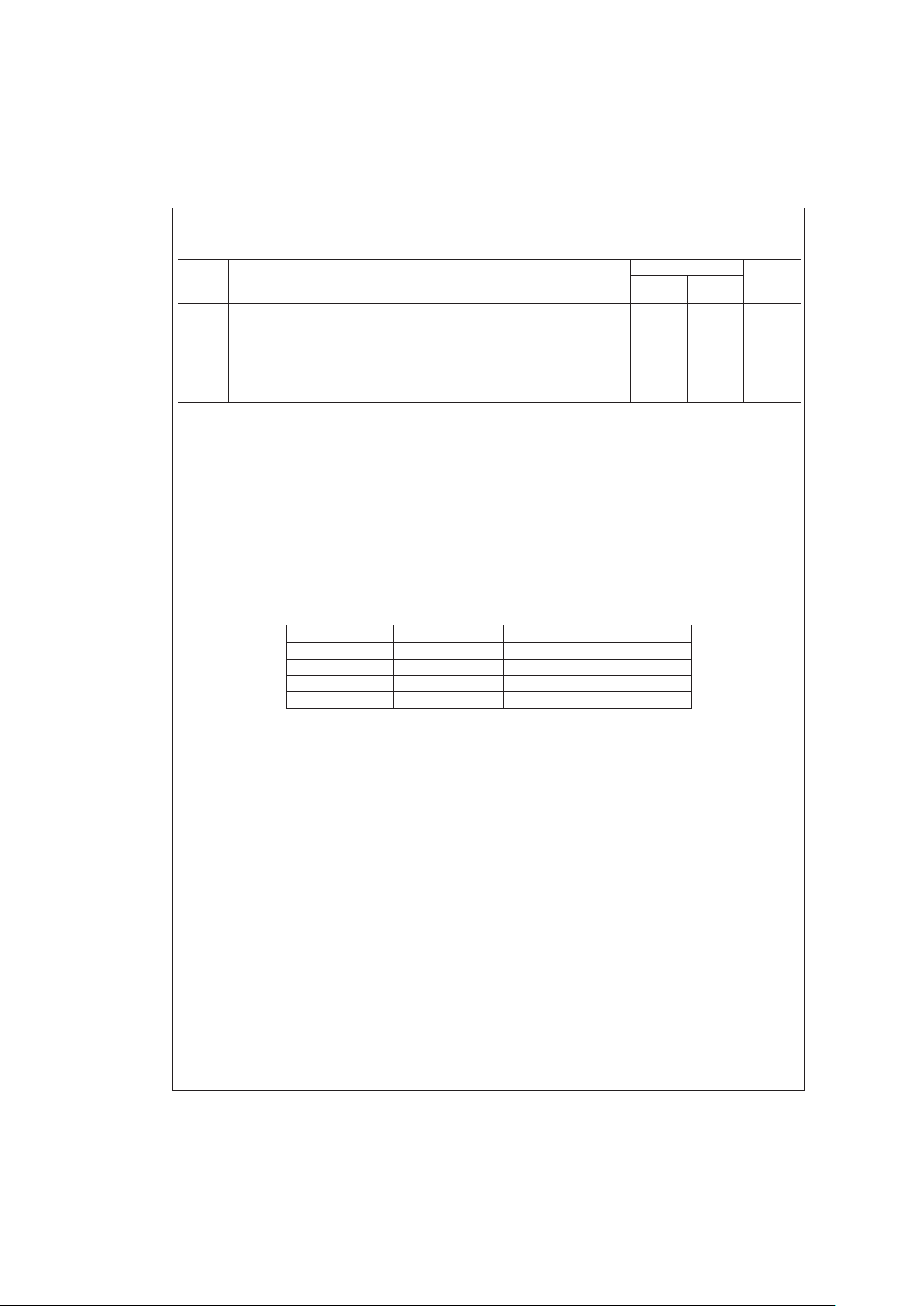
Electrical Characteristics (Notes 3, 4) (Continued)
The following specifications apply for VCC= +22V, and Volume@0 dB unless otherwise specified. Limits apply for TA= 25˚C.
Symbol Parameter Conditions
LM4753
Units
(Limits)
Typical
(Note 8)
Limit
(Note 9)
Standby
V
IL
Standby Low Input Voltage 0.8 V (max)
V
IH
Standby High Input Voltage 2.0 V (min)
Mute
V
IL
Mute Low Input Voltage 0.8 V (max)
V
IH
Mute High Input Voltage 2.0 V (min)
Note 1: DC Electrical Test.
Note 2: AC Electrical Test.
Note 3: Absolute Maximum Ratings indicate limits beyond which damage to the device may occur. Operating Ratings indicate conditions for which the device is
functional, but do not guarantee specific performance limits. Electrical Characteristics state DC and AC electrical specifications under particular test conditions
which guarantee specific performance limits. This assumes that the device is within the Operating Ratings. Specifications are not guaranteed for parameters where
no limit is given, however, the typical value is a good indication of device performance.
Note 4: All voltages are measured with respect to the ground (pin 8), unless otherwise specified.
Note 5: The maximum power dissipation must be derated at elevated temperatures and is dictated by T
JMAX
, θJA, and the ambient temperature, TA. The maximum
allowable power dissipation is PDMAX = (T
JMAX-TA
)/θJAor the number given in the Absolute Maximum Ratings, whichever is lower. For operating at case tempera-
tures above 25˚C, the device must be derated based on a 150˚C maximum junction temperature and a thermal resistance of θ
JC
= 5˚C/W (junction to case).
Note 6: Human body model, 100 pF discharged through a 1.5 kΩ resistor.
Note 7: Machine model, 200 pF–240 pF discharge through all pins.
Note 8: Typicals are measured at 25˚C and represent the parametric norm.
Note 9: Limits are guarantees that all parts are tested in production to meet the stated values.
Standby Mute Pin Function Table
Standby (Pin 9) Mute (Pin 10) Operating Condition
“L” or Open “L” Play
“L” or Open “H” or Open Mute
“H” “L” Standby
“H” “H” or Open Standby
www.national.com 4
Page 5

Typical Performance Characteristics
THD+N vs Frequency
DS100043-8
THD+N vs Frequency
DS100043-9
Output Power vs
Supply Voltage
DS100043-10
THD+N vs Frequency
DS100043-11
THD+N vs Frequency
DS100043-12
Output Power vs
Supply Voltage
DS100043-13
THD+N vs Output Power
DS100043-14
THD+N vs Output Power
DS100043-15
THD+N vs Output Power
DS100043-16
THD+N vs Output Power
DS100043-17
THD+N vs Output Power
DS100043-18
THD+N vs Output Power
DS100043-19
www.national.com5
Page 6

Typical Performance Characteristics (Continued)
Application Information
GENERAL FEATURES
The LM4753 has a number of valuable functions that make
this audio amplifier IC an all-in-one solution. The IC has a
stereo audio path from input to output with a DC voltage controlled volume attenuator in the preamp section. After the
volume attenuator is a line-out connection for preamp-out
control. The attenuation curve versus DC voltage can be
found by referring to the Volume Attenuation vs DC Voltage
graph in the Typical Performance Characteristics section.
The IC also possesses a mute function to provide audio attenuation as used on a remote control for a TV, as well as a
standby function for power conservation when not being
used. The IC is well protected with thermal shutdown and
output AC short circuit protection.
Mute Function
The muting function of the LM4753 allows the user to mute
the music going into the amplifier, providing over 60 dB of attenuation from input to output. The function is enabled by
placing a logic “1” or 5V onto the mute pin, pin 10. Todisable
the function, allowing music to be passed to the output, a
logic “0” or 0V should be placed on the mute pin. By placing
the device into mute mode, each of the power amplifier outputs are simultaneously muted. The DC volume control and
line-out amplifiers are not affected by the mute function.
Please refer to
Table 1
for each input condition.
To prevent mechanical switch bouncing from adversely affecting the functionality of the IC, an RC lowpass filter should
be used as shown in
Figure 2
. This circuit replaces the need
for a debounce circuit when using a mechanical switch to
control the IC logic functions. However, most systems typically utilize a microprocessor or COP microcontroller to interface with the logic control functions of the LM4753. When a
clean logic signal is used, as from a microcontroller, the RC
lowpass filter is not required.
Standby Function
The standby function allows the user to place the LM4753
into a power conserving mode that draws less than 10 mA of
quiescent power supply current. With the IC in this mode,
while using +22V for the supply voltage, the IC draws about
150 mW of power.
The standby function is enabled by placing a logic “1” or 5V
onto the standby pin, pin 9. To disable the function allowing
music to be passed to the output, a logic “0” or 0V should be
placed on the standby pin. When the standby function is en-
Supply Current
vs Supply Voltage
DS100043-20
Power Dissipation vs
Output Power
DS100043-21
Power Dissipation vs
Output Power
DS100043-22
Channel Separation
vs Frequency
DS100043-23
Attenuation vs Frequency
DS100043-24
Volume Attenuation vs
DC Voltage
DS100043-25
DS100043-26
FIGURE 2. Mute and Standby Pin Lowpass Filters
www.national.com 6
Page 7

Application Information (Continued)
abled, it overrides the mute function and places the IC in its
power conserving mode. If the mute function is enabled
while in standby mode, the IC will continue to remain in
standby mode. After the standby function is disabled, the IC
will be placed into mute mode. Please refer to the
Table1
for
each input condition.
TABLE 1. Mute and Standby Functional Conditions
Standby
(Pin 9)
Mute
(Pin 10)
Operating
Conditions
0V or open 0V Music Plays
0V or open 5V or open Mute Mode
5V 0V Standby Mode
5V 5V or open Standby Mode
To prevent mechanical switch bouncing from adversely affecting the functionality of an IC, an RC lowpass filter should
be used as shown in
Figure 2
. This circuit replaces the need
for a debounce circuit when using a mechanical switch to
control the IC logic functions. However, most systems typically utilize a microprocessor or COP microcontroller to interface with the logic control functions of the LM4753. When a
clean logic signal is used, as from a microcontroller, the RC
lowpass filter is not required.
DC Volume Control
The DC volume control for the LM4753 works between 0V
and 5V. When the volume pin (pin 3) is 0V, the IC’s preamp
stage is fully attenuated to 80 dB. When the volume pin is at
5V, the preamp stage passes audio at 0 dB.
The DC volume attenuation curve for the LM4753 is intended to provide smooth accurate attenuation changes at
higher DC voltages, but then attenuate fast to 80 dB at lower
DC voltages. This means that when the volume control is
turned down, the amplification is quickly attenuated, while at
normal listening levels, attenuation changes are more
gradual. Please refer to the VolumeAttenuation vs DC Voltage curve in the Typical Performance Characteristics section.
The DC voltage to pin 3 can be controlled with a potentiometer as shown in
Figures 1, 3
. A 100 kΩ resistor anda1µF
capacitor form an RC lowpass filter that keeps any unnecessary noise from coupling into the device. Any noise that is
coupled into the device is gained up by 40 dB.
Turn On/Off Characteristics
In order to minimize turn on and off pops, the LM4753 should
be powered up by using the sequence described below.
Figure 4
shows the sequence for turn on and off.
Since the power supply voltage of the power amplifier is
about 4 times more than a 5V power supply, it is assumed
that the logic voltage supply for the standby and mute functions is up before the large power supply reservoir capacitors
are charged. The LM4753 should be placed into standby
mode before the undervoltage protection circuitry is disabled. The undervoltage protection circuitry will keep the outputs of the LM4753 at 0V until the voltage from V
CC
to GND
is about 9.5V. If the standby function is disabled when the
supply voltage exceeds this value, the single-supply biasing
of the output stage will then begin to charge up to V
CC
/2. The
pop performance under this condition is quite good, however, it is highly recommended that the Mute and Standby
pin voltages are high at 5V while the main power supply voltage, V
CC
, is ramping up.
Once the main supply voltage is up to its full value, the
standby function can then be brought low to 0V. The biasing
of the amplifier and the output stage will then begin to charge
up to V
CC
/2. Notice that the supply current draw is approximately 7 mA until the standby function is disabled, at which
point, the supply current increases to approximately 13 mA
while in mute mode.
Once the single-supply biasing is established, the mute pin
voltage can be brought down to 0V,allowing the IC to amplify
the input signal.As shown in
Figure 4
, the input signal that is
applied to the IC all throughout the power-up process is not
passed to the speaker until the mute function is disabled.
The typical quiescent power supply current while in play
mode is approximately 80 mA.
The same sequence should be applied when powering down
the device. First the IC should be placed into mute mode,
muting the output, then placed into standby mode where the
bias and output coupling caps are gradually discharged to
ground. Once the biasing of the IC is brought to ground, the
main power supplies can be powered down. This power-up
and power-down sequence is highly recommended. Abrupt
changes in output current from enabling standby while the
output is driving an inductive load (like a speaker) may cause
the IC to handle extreme levels of power due to inductive
kickback. The IC may not be able to handle this and should
be avoided.
DS100043-27
FIGURE 3. Volume Pin Lowpass Filter
www.national.com7
Page 8

Application Information (Continued)
If the sequence described above and shown in
Figure 4
is
not used, then the external circuitry shown in Figure 5 should
be used to minimize turn-on/off pops and protect the output
stage against SOA violations.
In
Figure 5
there are only a few components that are different than the ones described earlier for lowpass filtering the
pin voltages. The new components are Q1, R2, R3, D1 and
D2. All of the other components will perform the same functions that were previously described.
The explanation of how the circuit in
Figure 5
works will be
related to the timing waveforms in
Figure 6
. The circuit in
Figure 5
protects the LM4753 from SOA violations by ensuring that the enabling of the standby function when music is
playing will not quickly bring the biasing to ground before the
input signal is smoothly attenuated through the volume function. Again, this is important because any quick changes in
output current when driving an inductive load will cause a flyback voltage that may damage the IC.
As shown in
Figure 6
, first notice that music is playing at the
output. When the mechanical standby switch is toggled from
ground (play mode) to 5V (standby mode), transistor Q1 is
quickly turned on, discharging capacitor C7, bringing the
voltage at the volume pin, pin 3, to ground. This quickly attenuates the audio signal at the output as shown in
Figure 6
.
While the input signal is being attenuated, the diode D1 becomes reverse biased and the voltage at the standby pin
starts to charge through R4, C8 and C9. There is also a finite
amount of current flowing through R5 as well, but because of
its high resistance, we can neglect it in the charge-up timing
of pin 9. Note that when the standby switch was grounded,
the diode D1 was clamping the standby pin low, setting the
initial voltage condition of C8 at a low voltage. Once C8
starts charging up, diode D2 becomes forward biased and
C9 also starts charging up. This brings the standby and mute
pin voltages up simultaneously. By the time the standby pin
voltage enables the standby function, the voltage at the volume pin will already have been ramped down to 0V and the
output signal will be close to 0V.
When the IC is in standby mode the biasing of the IC is
brought down to ground and the quiescent supply current is
around 7 mA. When the standby switch in
Figure 5
is toggled
DS100043-28
FIGURE 4. Turn-On/Off Sequence
www.national.com 8
Page 9

Application Information (Continued)
to ground for play mode, transistor Q1 is quickly cut off and
diode D1 is forward biased. When D1 is forward biased, capacitor C8 is quickly discharged to ground, bringing the
standby pin voltage to 0V. When C8 is discharged, diode D2
becomes reverse biased allowing capacitor C9 to discharge
to ground through R5. Diode D2 was clamping the voltage
on C9 to the same voltage as C8. Because R5 is 10 times
R4 it takes longer for the mute function to be disabled. While
the mute voltage is decreasing, the biasing of the amplifier is
charging up, since the standby function has already been
disabled. While the mute pin voltage is decreasing the volume pin voltage is slowly increasing through the charge-up
capacitor C7. Charging of the volume pin is from the 5V
through the volume control pot, R6 and C7. Notice that the
time constant of the volume pin charging is greater than the
mute pin discharging.As shown in
Figure 6
, the volume control function finally ramps up the input signal, allowing music
to be amplified at the output.
Please notice that with this circuit the standby switch will
override the mute switch as required in the IC’s functional
truth table in
Table 1
.
Also note once again that most systems typically utilize a microprocessor or COP microcontroller to interface with the
logic control functions of the LM4753. When a clean logic
signal is used, as from a microcontroller, RC lowpass filtering
is not required for the mute and standby functions.
DS100043-29
FIGURE 5. Turn-On/Off External Circuitry
www.national.com9
Page 10

Application Information (Continued)
Line Out
The line out function for the LM4753 is intended to provide
preamp output control for signal routing to an external power
amplifier.Anexample of this would be in a TV where the TV’s
remote control provides volume control on the audio signals
that may be sent to a home theater receiver.The line out amplifier is only able to drive high impedance loads like 2 kΩ
and 10 kΩ. Since the LM4753 utilizes a single +22V power
supply, the output of the line out amplifier is biased at
1
⁄2of
V
CC
or +11V. Because of this, its output should be capacitor
coupled to any other processing IC. The value of the capacitor is chosen by using
Equation (1)
.
f=1/2πRC (1)
where R is the processing IC input impedance and f is the
lowest audio frequency to be passed, like 20 Hz. The value
of capacitance is then calculated. For a 10 kΩ impedance,
C=1µF.
AC Short Circuit Protection
The LM4753 isAC short circuit protected with a current limiting setting minimum of 2.0A. Current limiting protection
works on AC waveforms only. DC shorts from the output to
ground are not protected. Generally this is not a concern as
there is a DC blocking capacitor on the output to protect the
speaker from single-supply DC bias.
Thermal Shutdown Protection
The LM4753 has a thermal shutdown protection scheme that
limits the drive capability of each amplifier output when the
internal die temperature reaches the temperature trip point
of 150˚C. The limiting of the output current drive capability is
proportional to increasing die temperature.
When the IC is in thermal shutdown mode, all of the DC biases of the IC remain unchanged. It is only the current drive
capability of the output power transistors that is limited. This
thermal shutdown mechanism provides for smooth audio attenuation rather than abruptly pulling the outputs to ground.
When the outputs are being limited, the maximum voltage
swing will be reduced, creating a clipping effect as shown in
Figure 7
. With further increases in die temperature the maxi-
mum voltage swing will be further reduced.
The thermal sensing mechanism monitors the global die
temperature and is not intended to operate quickly enough to
shutdown the IC for extremely high power dissipation pulses
created by driving very low impedance loads.
DS100043-30
FIGURE 6. Turn-On/Off External Circuitry Sequence
www.national.com 10
Page 11

Application Information (Continued)
In
Figure 7
, a 50 kHz input signal is used to show the clipping
and attenuating effect of the LM4753 when coming out of
thermal shutdown.
THERMAL CONSIDERATIONS
Determining Maximum Power Dissipation
It is important to determine the maximum amount of package
power dissipation in order to choose an adequate heat sink.
Improper heat sinking can lead to premature thermal shutdown operation, causing music to cut out.
Equation (2)
can
be used to calculate the approximate maximum integrated
circuit power dissipation for your amplifier design, given the
supply voltage, and rated load, with both channels being
driven simultaneously.
P
DMAX
=
2(V
CCtot
2
/2π2RL) (2)
To ensure that a proper heat sink is chosen, be sure to take
into account the effects of the unregulated power supply voltage variation and the highly reactive load impedance variation over frequency.
A poorly regulated power supply can have a supply voltage
variation of more than 10V. Be sure to take into account the
no-load power supply voltage.
A nominally rated 8Ω load can have an impedance dip down
to 5Ω at low frequencies. As well, the load is not purely resistive, and this causes the amplifier output current to be out of
phase with the output voltage. When the current and voltage
are out of phase, the internal power dissipation actually increases.
Equation (2)
can be directly applied to the Power Dissipation
vs Output Power curves in the Typical Performance Characteristics section. However, the curves take into account quiescent power dissipation which
Equation (2)
does not. The
curves are to be used as a guideline in determining the required heat sink and are not intended to provide exact power
dissipation values.
Heat Sinking
Choosing a heat sink for a high-power audio amplifier is
made entirely to keep the die temperature below its maximum junction temperature, so that the thermal protection circuitry does not operate under normal circumstances. The
heat sink should be chosen to dissipate the maximum IC
power for the maximum no-load supply voltage and the minimum load impedance.
Referring to
Figure 8
, the thermal resistance from the die
(junction) to the outside air (ambient) is a combination of
three thermal resistances, θ
JC
, θCSand θSA. Two of these
thermal resistances are provided by National, θ
JC
and θCS.
Since convection heat flow (power dissipation) is analogous
to current flow, thermal resistance is analogous to electrical
resistance, and temperature drops are analogous to voltage
drops, the power dissipation out of the LM4753 is equal to
the following:
P
DMAX
=
(T
JMAX–TAMB
)/θ
JA
(3)
The thermal resistance, θ
JA
is equal to θJC+ θCS+ θSA,
where θ
JC
is the junction-to-case thermal resistance, θCSis
the case-to-sink thermal resistance (thermal compound),
and θ
SA
is the sink-to-ambient thermal resistance.
Once the maximum power dissipation is calculated from
Equation (2)
above, the minimum heat sink thermal resis-
tance can be calculated from
Equation (4)
below.
θ
SA
=
[(T
JMAX–TAMB
)–P
DMAX(θJC
+ θCS)]/P
DMAX
(4)
Example:
V
CC
=
+22V
R
L
=
8Ω
θ
JC
=
1˚C/W
θ
CS
=
0.5˚C/W
(1) P
DMAX
=
2((22V)
2
/2π2(8Ω))=6W
(2) θ
SA
=
[(150˚C–25˚C) – 6W(1˚C/W + 0.5˚C/W)]/6W
=
19˚C/W
Therefore, the minimum heat sink thermal resistance re-
quired is 19˚C/W for both channels being driven simultaneously at maximum power dissipation into an 8Ω load using
a +22V voltage supply.Again, remember to take into account
the unregulated supply voltage and reactive load impedance
dips.
Should it be necessary to isolate the tab of the IC from the
heat sink, an insulating washer can be used. There are many
different types of insulating washers with varying thermal resistances. Good washers can be obtained from Thermalloy
or Berquist. Refer to the References list for contact information for these manufacturers.
Supply Bypassing
The LM4753 has good power supply rejection, however, for
all power amplifiers, proper power supply bypassing is required. To prevent oscillations and instability, all op amps
and power op amps should have their supply leads bypassed with low-inductance capacitors having short leads.
All high frequency bypass capacitors should be located as
close to the package terminals as possible and have a clear
unobstructed current return path to ground. It is typical to use
capacitor values that are a factor of 100 different from each
other to minimize interaction with each other. The LM4753
should be bypassed with 0.1 µF ceramic and 100 µF tantalum capacitors for optimum performance. The 100 µF tantalum can be replaced with an electrolytic, but the bypassing
DS100043-31
FIGURE 7. Thermal Shutdown Response
DS100043-32
FIGURE 8. Thermal Model
www.national.com11
Page 12

Application Information (Continued)
performance of the tantalum will be better. There should also
be large supply reservoir capacitors of about 4700 µF on
each supply rail. A larger reservoir capacitor will reduce the
supply ripple and will supply larger current burst requirements instead of requiring those large currents to come from
the main power supply transformer.
If adequate bypassing is not provided, the current in the supply leads, which is a rectified component of the load current,
may be fed back into internal circuitry.This signal may cause
signal distortion to increase.
Layout and Ground Loops
When designing a printed circuit board layout, it is important
to return the load ground, any output compensation ground,
and the low-level (feedback and input) grounds to the circuit
board common ground point through separate paths. Large
currents flowing along a ground conductor will generate voltages which effectively act as signals to the input ground ref-
erence. This can result in high frequency oscillation or excessive distortion. Output compensation components and
the high frequency supply bypass capacitors should be
placed as close as possible to the IC to reduce the effectsof
PCB trace resistance and inductance. For cases where long
traces must exist, widen the traces to minimize their inductance.
References
International Electronic Research Corporation
P.O. Box 7704,
Burbank, California 91510-7704,
(818) 842-7277
Thermalloy Inc.
P.O. Box 810839,
Dallas, Tx 75381-0839,
(214) 243-4321,
www.thermalloy.com
www.national.com 12
Page 13

Physical Dimensions inches (millimeters) unless otherwise noted
LIFE SUPPORT POLICY
NATIONAL’S PRODUCTS ARE NOT AUTHORIZED FOR USE AS CRITICAL COMPONENTS IN LIFE SUPPORT
DEVICES OR SYSTEMS WITHOUT THE EXPRESS WRITTEN APPROVAL OF THE PRESIDENT AND GENERAL
COUNSEL OF NATIONAL SEMICONDUCTOR CORPORATION. As used herein:
1. Life support devices or systems are devices or
systems which, (a) are intended for surgical implant
into the body, or (b) support or sustain life, and
whose failure to perform when properly used in
accordance with instructions for use provided in the
labeling, can be reasonably expected to result in a
significant injury to the user.
2. A critical component is any component of a life
support device or system whose failure to perform
can be reasonably expected to cause the failure of
the life support device or system, or to affect its
safety or effectiveness.
National Semiconductor
Corporation
Americas
Tel: 1-800-272-9959
Fax: 1-800-737-7018
Email: support@nsc.com
National Semiconductor
Europe
Fax: +49 (0) 1 80-530 85 86
Email: europe.support@nsc.com
Deutsch Tel: +49 (0) 1 80-530 85 85
English Tel: +49 (0) 1 80-532 78 32
Français Tel: +49 (0) 1 80-532 93 58
Italiano Tel: +49 (0) 1 80-534 16 80
National Semiconductor
Asia Pacific Customer
Response Group
Tel: 65-2544466
Fax: 65-2504466
Email: sea.support@nsc.com
National Semiconductor
Japan Ltd.
Tel: 81-3-5639-7560
Fax: 81-3-5639-7507
www.national.com
Staggered Lead Non-Isolated Package
NS Package Number TA15A
LM4753 Dual 10W Audio Power Amplifier w/Mute, Standby and Volume Control
National does not assume any responsibility for use of any circuitry described, no circuit patent licenses are implied and National reserves the right at any time without notice to change said circuitry and specifications.
 Loading...