

Page 1
January 2000
LM4663
2 Watt Stereo Class D Audio Power Amplifier with Stereo
Headphone Amplifier
LM4663 2 Watt Stereo Class D Audio Power Amplifier with Stereo Headphone Amplifier
General Description
The LM4663 is a fully integrated single supply, high efficiency Class D audio power amplifier solution. The LM4663
utilizes a continuous time delta-sigma modulation technique
that lowers output noise and THD when compared to conventional pulse width modulators.
The LM4663also features a stereo headphone amplifier that
delivers 80mW into a 32Ω headset with lessthan 0.5%THD.
The LM4663 has two stereo inputs that can be selected to
drive either the headphone amplifier or the Class D amplifier.
All amplifiers are protected with thermal shutdown.
In standby mode, the LM4663 draws an extremely low 2µA
supply current. With a 4Ω load, the IC’s efficiency for a
250mW power level is 69%, reaching 83%at a power level
of 2W. The IC features click and pop reduction circuitry that
minimizes audible popping during device turn-on and
turn-off. The LM4663 is available in a 24-lead TSSOP package, ideal for portable and desktop computer applications.
Key Specifications
n POat THD+N=1
n THD+N at 1kHz at 1 Watt into 4Ω (Power
Amp) 0.2%(typ)
%
2.1W (typ)
n Efficiency at 2 Watt into 4Ω 83%(typ)
n Efficiency at 250mW into 4Ω 69%(typ)
n Total quiescent power supply current 22mA (typ)
n Total shutdown power supply current 2µA (typ)
n THD+N 1kHz, 20mW, 32Ω (Headphone) 0.15%(typ)
n Single supply range 4.5V to 5.5V
Features
n Delta-sigma modulator.
n Two stereo input selector.
n “Click and pop” suppression circuitry.
n Micropower shutdown mode.
n 24 lead TSSOP package (No heatsink required).
n Stereo headphone amplifier.
Applications
n Portable computers
n Desktop computers
n Multimedia Monitors
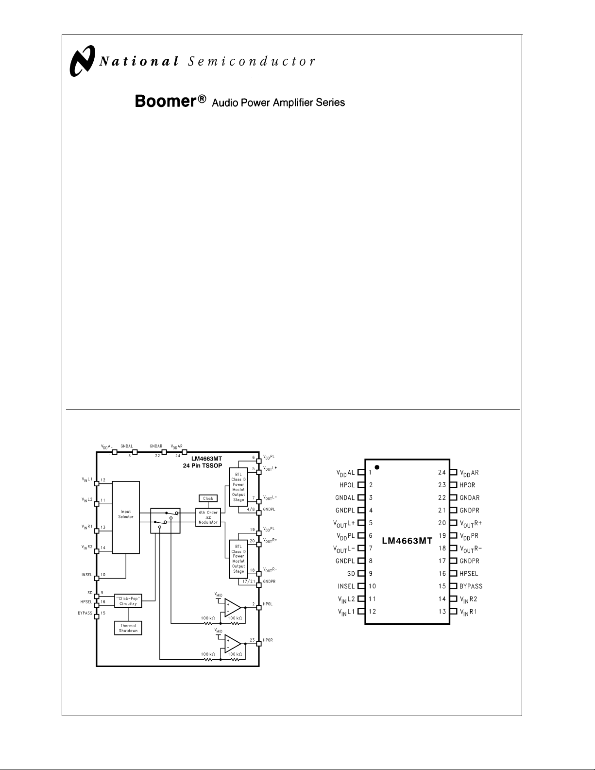
Block Diagram Connection Diagram
TSSOP Package
DS101269-2
Top View
Order Number LM4663MT
See NS Package Number MTC24
DS101269-1
BOOMER™is a trademark of National Semiconductor Corporation.
© 2000 National Semiconductor Corporation DS101269 www.national.com
(TSSOP Package)
Page 2
Absolute Maximum Ratings (Note 2)
If Military/Aerospace specified devices are required,
LM4663
please contact the National Semiconductor Sales Office/
Distributors for availability and specifications.
Supply Voltage 6.0V
Input Voltage −0.3V to V
DD
+0.3V
Power Dissipation (Note 3) Internally Limited
Load Resistance 2.5Ω, min
ESD Susceptibility(Note 4) 2000V
Pins 5,7,18,20 600V
ESD Susceptibility (Note 5) 200V
Pins 5,7,18,20 50V
Junction Temperature (Note 6) 150˚C
Storage Temperature −65˚C ≤ T
≤ 150˚C
A
Electrical Characteristics (Notes 1, 2, 7)
The following specifications apply for V
Limits apply for T
= 25˚C.
A
=
DD
Symbol Parameter Conditions
V
S
I
S
I
S
I
SD
R
IN
V
IH
V
IL
V
IH
V
IL
Operating Supply Voltage
Range
Quiescent Power Supply
Current, Class D Mode
Quiescent Power Supply
Current, Headphone Mode
Quiescent Power Supply
Current, Shutdown Mode
Input Resistance in Both Modes 20 kΩ
Minimum High Level Input
Voltage
Maximum Low Level Input
Voltage
Minimum High Level Input
Voltage
Maximum Low Level Input
Voltage
Power Amplifiers
P
R Output Power, Per Channel THD+N ≤ 1%,f
O
P
D1
P
D2
P
D3
E
FF1
E
FF2
E
FF3
Power Dissipation P
Power Dissipation P
Power Dissipation P
Efficiency P
Efficiency
Efficiency P
THD+N Harmonic Distortion + Noise P
V
NOISE
PSRR
A
V
A
L−AVR Stereo Gain Tracking 1kHz, V
V
Output Noise Voltage, RMS.
A−Weighted
Power Supply Rejection Ratio
(Referred to Input)
Voltage Gain 1kHz, V
=
5V, R
4Ω, LC filter values as shown in Figure 1, unless otherwise specified.
L
=
V
0V
IN
RMS,VHPSEL
=
V
0V
IN
RMS,VHPSEL
=
V
5V 2 µA
SD
Shutdown Pin & Input Select
Pin
Shutdown Pin & Input Select
Pin
Headphone Select Pin 4.5 V
Headphone Select Pin 0.5 V
=
2W/Chan, f
O
=
1W/Chan, f
O
=
.25W/Chan, f
O
=
2W/Chan, f
O
=
1W/Chan, R
P
O
1kHz
=
.25W/Chan, f
O
=
1W/Chan, f
O
R
SOURCE
=
BW=8Hz to 22kHz
200mV, 1kHz, V
=
IN
=
IN
Soldering Information
TSSOP Package
Vapor Phase (60 sec.) 215˚C
Infrared (15 sec.) 220˚C
See AN-450 “Surface Mounting and their Effects on
Product Reliability” for other methods of soldering surface
mount devices.
Operating Ratings(Notes 1, 2)
Temperature Range
T
≤ TA≤ T
MIN
MAX
Supply Voltage 4.5V ≤ V
Thermal Resistance (TSSOP Package)
θ
JA
θ
JC
LM4663
Typical Max Min
5 5.5 4.5 V
=
0V 22 35 mA
=
V
S
510 mA
0.5 V
=
1kHz 2.1 W
IN
=
1kHz 0.82 W
IN
=
1kHz 0.49 W
IN
=
1kHz 0.23 W
IN
=
1kHz 83
IN
L
IN
IN
50Ω,C
IN
=
IN
100mV, R
100mV, R
=
=
=
044
=
8Ω,f
IN
85 80
1kHz 69
1kHz 0.2
=
1µF,
=
4Ω 13 dB
L
=
4Ω 0.1 dB
L
200 µV
−40˚C ≤ TA≤ +85˚C
≤ 5.5V
DD
80˚C/W
20˚C/W
Units
4.5 V
%
%
%
%
dB
www.national.com 2
Page 3
Electrical Characteristics (Notes 1, 2, 7) (Continued)
The following specifications apply for V
Limits apply for T
= 25˚C.
A
=
DD
Symbol Parameter Conditions
Headphone Amplifiers
P
O
Power Out Per Channel THD+N ≤ 1%,R
THD+N Distortion + Noise
V
NOISE
PSRR
A
V
A
L−AVR Stereo Gain Tracking 1kHz, V
V
Note 1: All voltages are measured with respect to the ground pin, unless otherwise specified.
Note 2:
functional, but do not guarantee specific performance limits.
guarantee specific performance limits. This assumes that the device iswithin the Operating Ratings. Specifications are not guaranteed for parameters where no limit
is given, however, the typical value is a good indication of device performance.
Note 3: For operating at case temperatures above 25˚C, the device must be derated based on a 150˚C maximum junction temperature and a thermal resistance of
= 80˚C/W (junction to ambient).
θ
JA
Note 4: Human body model, 100 pF discharged through a 1.5 kΩ resistor.
Note 5: Machine Model 220pF−240pF discharged through all pins.
Note 6: The operating junction temperature maximum is 150˚C.
Note 7: Limits are guaranteed to National’s AOQL (Average Outgoing Quality Level).
Output Noise Voltage, RMS
Power Supply Rejection Ratio
(Referred to Input)
Voltage Gain 1kHz, V
“Absolute Maximum Ratings”
indicate limits beyond which damage to the device may occur.
=
5V, R
4Ω, LC filter values as shown in Figure 1, unless otherwise specified.
L
1kHz
=
P
20mW, R
O
1kHz
=
50Ω,C
R
IN
IN
8Hz to 22kHz
200mV, 1kHz, V
32Ω
=
100mV, R
IN
=
100mV, R
IN
“Electrical Characteristics”
LM4663
Typical Max Min
=
32Ω,f
L
=
32Ω,f
L
=
1µF, BW
=
0, R
IN
state DC andACelectricalspecificationsunderparticulartestconditionswhich
=
IN
=
IN
=
=
L
=
32Ω 5.5 dB
L
=
32Ω 0.1 dB
L
80 60
0.15
30 µV
44 dB
“Operating Ratings”
indicate conditions for which the device is
Units
mW
LM4663
%
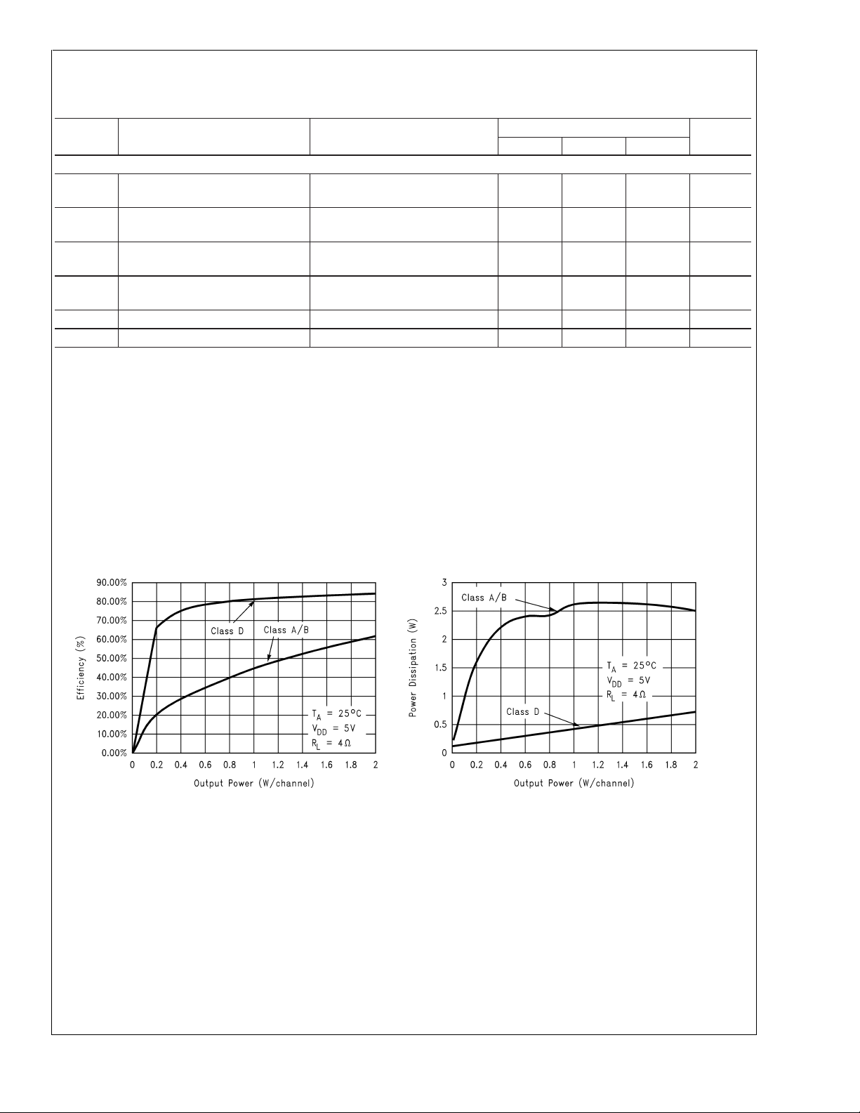
Typical Performace Characteristics
Efficiency vs Output Power
DS101269-10
Power Dissipation vs Output Power
DS101269-11
www.national.com3
Page 4

Typical Performace Characteristics (Continued)
LM4663
Class D Amplifier
In-Band Output Spectrum
Class D Amplifier
In-Band Output Spectrum
Class D Amplifier
THD+NvsPower vs Frequency
Headphone THD+NvsFrequency vs Power
DS101269-12
DS101269-14
DS101269-13
Class D Amplifier
THD+NvsFrequency vs Power
DS101269-15
www.national.com 4
DS101269-16
Page 5

Applications Information
LM4663
DS101269-3
FIGURE 1. Operating on a single 5V supply, this recommended application circuit is a complete solution with 2W
Class D amplifiers that drive 4Ω speakers and 80mW amplifiers drive 32Ω headphones.
Suggested Application Circuit
The LM4663 achieves its specified performance using the
recommended application circuit shown in Figure 1. The circuit provides fullaccess to the stereo 2W/channelpower amplifiers and the 80mW/channel stereo headphone amplifier.
The HPSELECT (headphone select ) input is controlled by a
stereo mini-plug/jack with additional control contact. Other
applications of this device may use external generated logic
signals to control this function.
Control Pins
The LM4663 has three controlpins: INSEL, SD, and HPSEL.
The INSEL pin is used to select between the two stereo inputs, V
supply selects V
V
IN2
IN1
and V
. Connecting the INSEL pin to the positive
IN2
, whereas pulling it to ground selects
IN1
. Micropower shutdown operation is selected by pulling
the SD to the positive supply.Applying the positive supply to
the HPSEL pin selects the headphone amplifiers and
grounding the HPSEL pin selects the Class D amplifiers.
Table 1 is a summary of the function selected when applying
ground or V
to the control pins.
DD
TABLE 1. Function selected when applying V
GND to the INSEL, SD, and HPSEL control pins.
Control
Function
INSEL 10 V
SD 9 Full power
HPSEL 16 Deactivate
Pin Apply GND Apply V
L&R V
IN1
IN2
L&R
Micropower
operation
shutdown
Deactivate Class
headphone amps
and activate
Class D amps
D amps and
activate
headphone amps
Output Filters
The LM4663’s 2W power amplifiers use a Class D switching
topology that requires a filter between the amplifier outputs
and the load.The balanced, L-C filters shownin Figure 1 use
component values recommended fora maximally flat magnitude in the pass-band and a cut-off frequency of 18kHz with
a load impedance of 4Ω. We do not recommend omitting the
filter because considerable out-of-band energy is present in
the Class D output waveform. This energy would be dissipated in the load impedance’s resistive component, which
diminishes efficiency.
or
DD
DD
www.national.com5
Page 6

Applications Information (Continued)
Bypass Pin Capacitor
LM4663
In order to achieve the largest unclipped output voltage
swing, a DC reference voltage for the circuit is derived internally by a resistor divider from the power supply voltage. To
reduce sensitivity to audio frequency variations on the reference voltage, a de-coupling capacitor is recommended between the BYPASS pin andthe best availableAC ground reference. This is typically the shield connection from the signal
source. A poor choice is the power ground because considerable current flows from the LM4663 through pins 4,8,17,
and 21 to the power supply return.This current is rich in harmonic frequencies related to the input audio frequency.
These harmonics can easily couple into the signal path by
sharing power ground conductors with the bypass capacitor
connection. The result is increased THD.
Minimum Load Resistance
As specified in the Absolute Maximum Ratings, the minimum
load resistance supported by theLM4663 at the output ofthe
filters is 2.5 Ohms. Loads (usually loudspeakers) should be
tested over the audio band to determinewhether ornot there
are resonant points of diminshed impedance less than this
limit.
Output Filter Components
Table 2 shows suggested standard values of the capacitor
(C) and the inductor (L) used in Figure 1’s output filter for 4Ω
and 8Ω loads. The bandwidth for each case is typically
18kHz.
the power amp outputs and their associated pins. Short connections reduce inductance and EMI radiation from the output switching currents. Also, the distance from the switching
outputs to the filter inductors is similarly minimized to reduce
radiated noise. Table 4 is the recommended circuit’s
bill-of-materials (BOM). Figure 8 is a photograph of the recommended four-layer PC board.
The board is designed foruse with an external 5Vsupply,4Ω
speakers, and 32Ω headphones.Apply the supply voltage to
the V
channel speaker between the Lout+ and Lout− pads and the
right channel speaker between the Rout+ and Rout− pads.
Connect the left and right headphone speakers to the HPL
and HPR pads, respectively. The board has two sets of HPL
and HPR pads. Use the set found across the top edge for a
headphone jack like that shown in Figure 1. The other set
found along the right edge can be used for a three terminal
headphone jack. Ensure that a speaker’s + terminal is connected to an amplifier’s + output. This preserves the phase
relationship between the left and right channels.
The board accepts two stereo inputs. Apply channel 1’s right
and left input signals to the Rin1 and Lin1 pads,respectively.
Apply channel 2’s right and left input signals to the Rin2 and
Lin2 pads, respectively.
The board’s bottom edge has seven jumpers. From left to
right, these jumpers select micropower shutdown, input
channel, headphone amplifier, Class D amplifier, and headphone amplifier when plugging in headphones. Table 3 is a
guide for selecting the various functions.
pad and ground to the GND pad. Connect the left
DD
TABLE 2. Output filter component values for different
load resistance.
Load Resistance (Ω) Capacitor C (µF) Inductor L (µH)
4222
8144
Short Circuit Tolerance
The LM4663, when used in the recommended application
circuit, is tolerant of limited duration short circuit connections
between the filtered positive and negative outputs. Shorts
from either output to ground or supply voltage, or from the
unfiltered outputs to any other low impedance node can result in permanent damage to the IC.
Start-up Current
The LM4663 exhibits abnormally high quiescent current
drain when the supply voltage is below the specified operating range of 4.5 to 5.5V. It is, therefore, recommended that
the IC be initially powered up in the shutdown mode (SD
V
). Normal application of power from laboratory bench
DD
supplies is not usually a problem unless the current limit of
the supply is set too low (
have a much lower current capability (such as USB applications). In these cases power must be applied with shutdown
asserted and switched to the operating mode after power is
present and settled. An external circuit that provides this
condition automatically is given in Figure 2, and is recommended for those current-critical applications.
Printed Circuit Board Layout
Figures 3 through 7 show the layout of a recommended
four-layer PC board that is optimized for the LM4663 and associated external components. This layoutemphasizes short
connections between the power reservoir capacitors near
<
1A); however, some applications
TABLE 3. These are the functions selected by the
jumpers on the recommended PC board.
Jumper Function
SD-L Shorting selects normal operation.
SD-H Jumper is open.
SD-H Shorting activates shutdown:
micropower operation.
SD-L Jumper is open.
INSEL-L Shorting selects stereo input 1.
INSEL-H Jumper is open.
INSEL-H Shorting selects stereo input 2.
INSEL-L Jumper is open.
Class AB Shorting activates the headphone
amplifier and deactivates the Class D
amplifier. Class D and HP jack
=
Class D Shorting activates the Class D amplifier
HP Jack Shorting allows the act of plugging in
jumpers are open
and deactivates the headphone
amplifier. Class AB and HP jack
jumpers are open
headphones to activate the headphone
amplifier and deactivate the Class D
amplifier. Removing headphones
restores Class D amplifier operation and
deactivates the headphone amplifier.
Class AB and Class D jumpers are
open. (Requires the use of a headphone
jack like that shown in Figure 1.)
www.national.com 6
Page 7

Applications Information (Continued)
DS101269-4
FIGURE 2. At power-up, the LP3740 forces the LM4663 into shutdown, which prevents abnormal quiescent current
flow through the amplifier. Once V
rises above 4V and after a 200ms delay set by C1, normal amplifier operation is
CC
restored.
LM4663
DS101269-5
FIGURE 3. Recommended PC board layout:
Component side silkscreen
DS101269-6
FIGURE 4. Recommended PC board layout:
Component side layout
DS101269-7
FIGURE 5. Recommended PC board layout: Inner
Layer ground plane layout
DS101269-8
FIGURE 6. Recommended PC board layout: Inner
Layer supply plane layout
www.national.com7
Page 8

Applications Information (Continued)
LM4663
DS101269-9
FIGURE 7. Recommended PC board layout: Bottom side layout
TABLE 4. Suggested PC Board Bill-of-Materials for recommended PC boards. (See Figures 1 and 3 through 7)
Component Footprint Type Value Size Comment
C1-C4 0805 SMD/Top 1µF
C5-C7 7243 SMD/Top 220µF ’D’ Tan./10V
C8,C10,C12,C14 0805 SMD/Top .47µF
C9,C11,C13,C15 3216 SMD/Top 2.2µF ’A’ Tan.
C16-C18 0805 SMD/Top 1µF
C19-C22 0805 SMD/Bot 1µF No Silkscreen
R5a,R6a 0805 SMD 100k
R7a 0805 SMD 1k
L1-L4 D03316P−223 SMD 22µH Coilcraft: (847)639−6400
U1 LM4663MT TSSOP 24 Pin National 2W Class D amplifier
http://www.coilcraft.com
www.national.com 8
Page 9

Applications Information (Continued)
LM4663
FIGURE 8. Recommended LM4663 PC Board
DS101269-35
www.national.com9
Page 10

Physical Dimensions inches (millimeters) unless otherwise noted
Order Number LM4663MT
NS Package Number MTC24
LIFE SUPPORT POLICY
NATIONAL’S PRODUCTS ARE NOT AUTHORIZED FOR USE AS CRITICAL COMPONENTS IN LIFE SUPPORT
DEVICES OR SYSTEMS WITHOUT THE EXPRESS WRITTEN APPROVAL OF THE PRESIDENT AND GENERAL
COUNSEL OF NATIONAL SEMICONDUCTOR CORPORATION. As used herein:
1. Life support devices or systems are devices or
systems which, (a) are intended for surgical implant
into the body, or (b) support or sustain life, and
whose failure to perform when properly used in
accordance with instructions for use provided in the
2. A critical component is any component of a life
support device or system whose failure to perform
can be reasonably expected to cause the failure of
the life support device or system, or to affect its
safety or effectiveness.
labeling, can be reasonably expected to result in a
LM4663 2 Watt Stereo Class D Audio Power Amplifier with Stereo Headphone Amplifier
significant injury to the user.
National Semiconductor
Corporation
Americas
Tel: 1-800-272-9959
Fax: 1-800-737-7018
Email: support@nsc.com
www.national.com
National does not assume any responsibility for use of any circuitry described, no circuit patent licenses are implied and National reserves the right at any time without notice to change said circuitry and specifications.
National Semiconductor
Europe
Fax: +49 (0) 1 80-530 85 86
Email: europe.support@nsc.com
Deutsch Tel: +49 (0) 1 80-530 85 85
English Tel: +49 (0) 1 80-532 78 32
Français Tel: +49 (0) 1 80-532 93 58
Italiano Tel: +49 (0) 1 80-534 16 80
National Semiconductor
Asia Pacific Customer
Response Group
Tel: 65-2544466
Fax: 65-2504466
Email: sea.support@nsc.com
National Semiconductor
Japan Ltd.
Tel: 81-3-5639-7560
Fax: 81-3-5639-7507
 Loading...