

Page 1
August 2000
LM4651 & LM4652 Overture
LM4651 & LM4652
Overture
™
Audio Power Amplifier
170W Class D Audio Power Amplifier Solution
General Description
The IC combination of the LM4651 driver and the LM4652
power MOSFET provides a high efficiency, Class D subwoofer amplifier solution.
The LM4651 is a fully integrated conventional pulse width
modulator driver IC. The IC contains short circuit, under
voltage, over modulation, and thermal shut down protection
circuitry. It contains a standby function, which shuts down
the pulse width modulation and minimizes supply current.
The LM4652 is a fully integrated H-bridge power MOSFET
IC in a TO-220 power package. Together, these two IC’s
form a simple, compact high power audio amplifier solution
complete with protection normally seen only in Class AB
amplifiers. Few external components and minimal traces
between the IC’s keep the PCB area small and aids in EMI
control.
The near rail-to-rail switching amplifier substantially increases the efficiencycompared to Class AB amplifiers. This
high efficiency solution significantly reduces the heat sink
size compared to a Class AB IC of the same power level.
This two-chip solution is optimum for powered subwoofers
and self powered speakers.
Key Specifications
n Output power into 4Ω with<10% THD. 170W (Typ)
n THD at 10W, 4Ω, 10 − 500Hz.
n Maximum efficiency at 125W 85% (Typ)
n Standby attenuation.
Features
n Conventional pulse width modulation.
n Externally controllable switching frequency.
n 50kHZ to 200kHz switching frequency range.
n Integrated error amp and feedback amp.
n Turn−on soft start and under voltage lockout.
n Over modulation protection (soft clipping).
n Short circuit current limiting and thermal shutdown
protection.
n 15 Lead TO−220 isolated package.
n Self checking protection diagnostic.
Applications
n Powered subwoofers for home theater and PC’s
n Car booster amplifier
n Self-powered speakers
<
0.3% THD (Typ)
>
100dB (Min)
™
170W Class D Audio Power Amplifier Solution
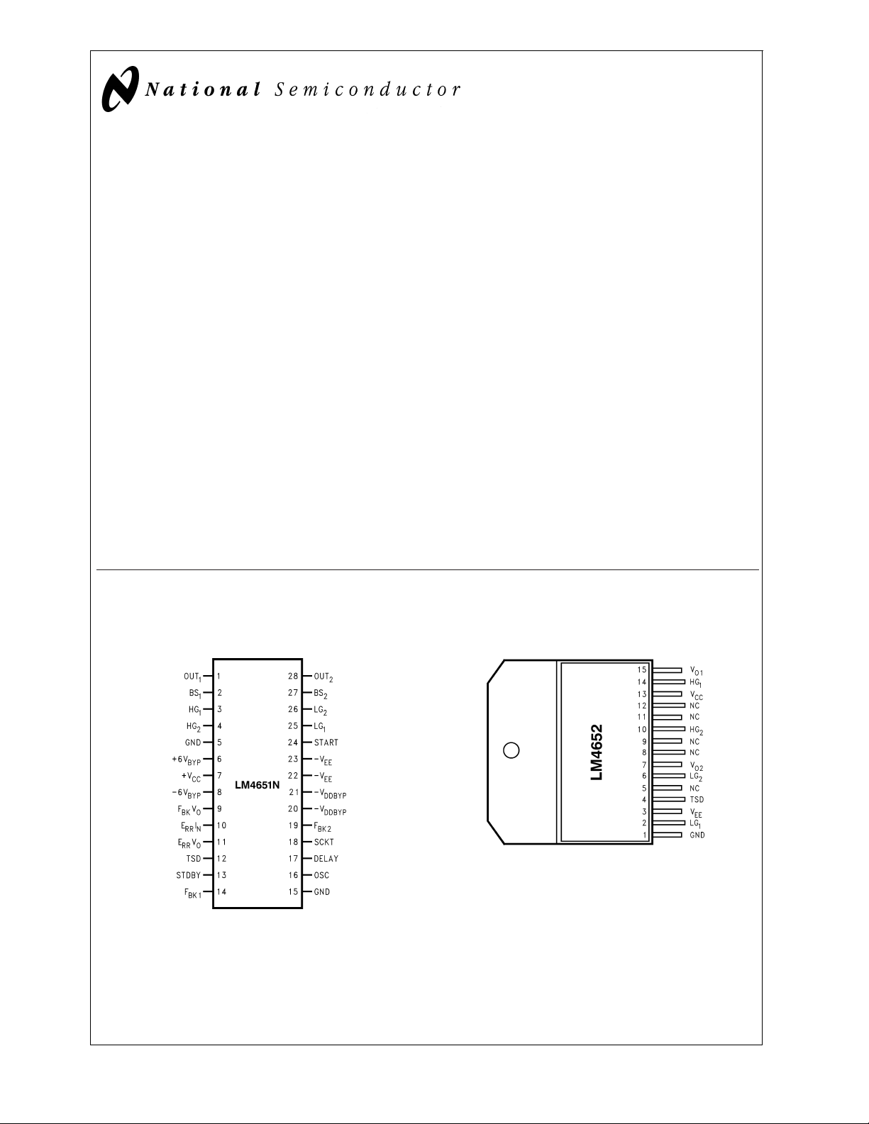
Connection Diagrams
LM4651 Plastic Package
Top View
Order Number LM4651N
See NS Package Number N28B
DS101277-72
LM4652 Plastic Package (Note 8)
DS101277-73
Isolated TO-220 Package
Order Number LM4652TF
See NS Package Number TF15B
or
Non-Isolated TO-220 Package
Order Number LM4652TA
See NS Package Number TA15A
Overture®is a registered trademark of National Semiconductor Corporation.
© 2001 National Semiconductor Corporation DS101277 www.national.com
Page 2
Absolute Maximum Ratings (Notes 1, 2)
If Military/Aerospace specified devices are required,
please contact the National Semiconductor Sales Office/
Distributors for availability and specifications.
Supply Voltage
Output Current (LM4652) 10A
LM4651 & LM4652
Power Dissipation (LM4651) (Note 3) 1.5W
Power Dissipation (LM4652) (Note 3) 32W
±
22V
Operating Ratings (Notes 1, 2)
Temperature Range −40˚C ≤ T
Supply Voltage |V
Thermal Resistance
LM4651 N Package
θJA 52˚C/W
θJC 22˚C/W
+
|+|V−| 22V to 44V
ESD Susceptibility (LM4651) (Note 4) 2000V
LM4652 (pins 2,6,10,11) 500V
ESD Susceptibility (LM4651) (Note 5) 200V
LM4652 (pins 2,6,10,11) 100V
LM4652 TF, TO−220 Package
θJA 43˚C/W
θJC 2.0˚C/W
Junction Temperature (Note 6) 150˚C
Soldering Information
N, TA and TF Package (10 seconds) 260˚C
Storage Temperature −40˚C to + 150˚C
LM4652 T, TO−220 Package
θJA 37˚C/W
θJC 1.0˚C/W
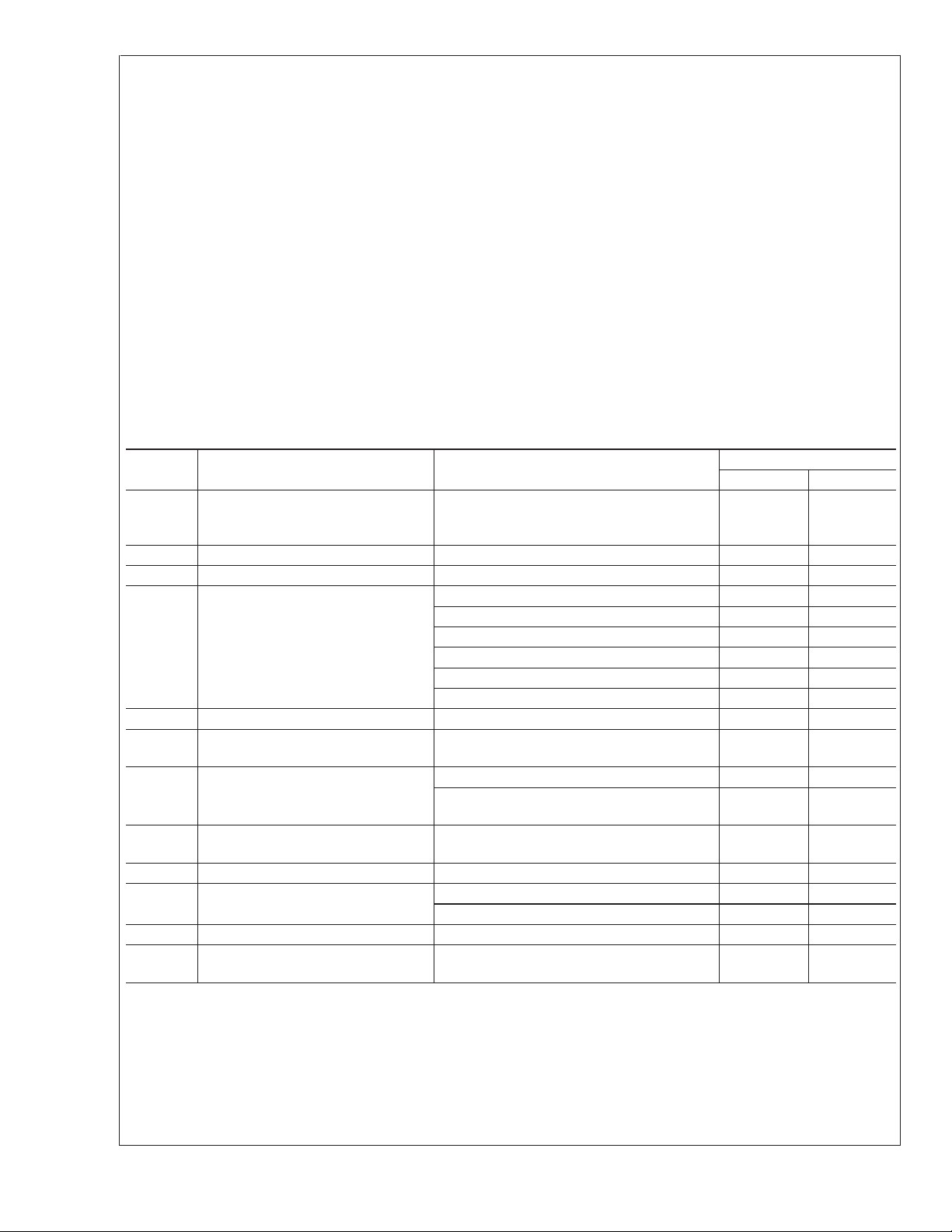
System Electrical Characteristics for LM4651 and LM4652 (Notes 1, 2)
The following specifications apply for +VCC= +20V, −VEE= −20V, fSW= 125kHz, fIN= 100Hz, RL=4Ω, unless otherwise
specified. Typicals apply for T
Symbol Parameter Conditions
I
CQ
I
STBY
A
P
M
O
Total Quiescent Power Supply
Current
Standby Current V
Standby Attenuation V
Output Power (Continuous Average)
η Efficiency at P
η
Pd
Efficiency
(LM4651 & LM4652)
Power Dissipation
(LM4651 + LM4652)
THD+N Total Harmonic Distortion Plus Noise
e
OUT
Output Noise A Weighted, no signal, RL=4Ω 550 µV
SNR Signal-to-Noise Ratio
V
OS
Output Offset Voltage VIN= 0V, IO= 0mA, R
PSRR Power Supply Rejection Ratio
= 25˚C. For specific circuit values, refer to Figure 1 (Typical Audio Application Circuit).
A
Typical Units
= 0V, LO= 0mA, |I
V
CIN
R
DLY
R
DLY
13 = 5V, Stby: On 17 mA
PIN
13 = 5V, Stby: On
PIN
R
=4Ω, 1% THD 125 W
L
R
=4Ω, 10% THD 155 W
L
R
=8Ω, 1% THD 75 W
L
R
=8Ω, 10% THD 90 W
L
f
= 75kHz, RL=4Ω, 1% THD 135 W
SW
f
= 75kHz, RL=4Ω, 10% THD 170 W
SW
=5W PO= 5W, R
O
= 125W, THD = 1% 85 %
P
O
= 125W, THD = 1% (max) 22 W
P
O
f
= 75kHz, PO= 135W,
SW
=0Ω
= 10kΩ
=5kΩ 55 %
DLY
VCC+
|+|I
VEE−
|
THD = 1% (max)
10W, 10Hz ≤ f
≤ 500Hz, AV=18dB
IN
10Hz ≤ BW ≤ 80kHz
A-Wtg, P
22kHz BW, P
=4Ω, 10Hz ≤ BW ≤ 30kHz
R
L
+V
CC
= 125W, RL4Ω 92 dB
out
= 125W, RL4Ω 89 dB
out
=0Ω 0.7 V
OFFSET
AC
=−V
=1V
EE
RMS,fAC
AC
= 120Hz
LM4651 & LM4652
237
124
>
115 dB
22 W
0.3 %
37 dB
≤ +85˚C
A
mA
mA
www.national.com 2
Page 3
Electrical Characteristics for LM4651 (Notes 1, 2, 7)
The following specifications apply for +VCC= +20V, −VEE= −20V, fSW= 125kHz, unless otherwise specified. Limits apply for
T
= 25˚C. For specific circuit values, refer to Figure 1 (Typical Audio Application Circuit).
A
Symbol Parameter Conditions
I
CQ
Standby
V
IL
V
IH
f
SW
f
SWerror
T
dead
T
OverMod
Total Quiescent Current
Standby Low Input Voltage Not in Standby Mode 0.8 V
Standby High Input Voltage In Standby Mode 2.5 2.0 V
Switching Frequency Range
50% Duty Cycle Error R
Dead Time R
Over Modulation Protection Time Pulse Width Measured at 50% 310 ns
LM4652 not connected, I
|+|I
|I
VCC+
R
= 15kΩ 65 kHz
OSC
R
=0Ω 200 kHz
OSC
=4kΩ,fSW= 125kHz 1 3 %
OSC
=0Ω 27 ns
DLY
VEE−
|, R
DLY
O
=0Ω
= 0mA,
Min Typical Max Units
15 36 45 mA
LM4651
Electrical Characteristics for LM4652 (Notes 1, 2, 7)
The following specifications apply for +VCC= +20V, −VEE= −20V, unless otherwise specified. Limits apply for TA= 25˚C. For
specific circuit values, refer to Figure 1 (Typical Audio Application Circuit).
Symbol Parameter Conditions
DSS
V
(BR)
I
DSS
VGS
th
R
DS(ON)
t
r
t
f
I
D
Note 1: Absolute Maximum Ratings indicate limits beyond which damage to the device may occur. Operating Ratings indicate conditions for which the device is
functional, but do not guarantee specific performance limits. Electrical Characteristics state DC and AC electrical specifications under particular test conditions which
guarantee specific performance limits. This assumes that the device is within the Operating Ratings. Specifications are not guaranteed for parameters where no limit
is given, however, the typical value is a good indication of device performance.
Note 2: All voltages are measured with respect to the GND pin unless otherwise specified.
Note 3: For operating at case temperatures above 25˚C, the LM4651 must be de−rated based on a 150˚C maximum junction temperature and a thermal resistance
of θ
2.0 ˚C/W (junction to case) for the isolated package (TF) or a thermal resistance of θ
Note 4: Human body model, 100 pF discharged through a 1.5 kΩ resistor.
Note 5: Machine Model, 220pF-240pF discharge through all pins.
Note 6: The operating junction temperature maximum, T
Note 7: Limits are guaranteed to National’s AOQL (Average Outgoing Quality Level).
Note 8: The LM4652TA package TA15A is a non-isolated package, setting the tab of the device and the heat sink at −V potential when the LM4652 is directly
mounted to the heat sink using only thermal compound. If a mica washer is used in addition to thermal compound, θ
will be isolated from −V.
Drain−to−Source Breakdown
Voltage
VGS = 0 55 V
Drain−to−Source Leakage Current VDS = 44VDC, VGS = 0V 1.0 mA
Gate Threshold Voltage VDS = VGS, ID = 1mA
Static Drain−to−Source On
Resistance
Rise Time
Fall Time
Maximum Saturation Drain
Current
= 62 ˚C/W (junction to ambient), while the LM4652 must be de−rated based on a 150˚C maximum junction temperature and a thermal resistance of θJC=
JA
VGS=6V
VGD=6V
=0Ω
VGD=6V
=0Ω
VGS=6V
is 150˚C.
jmax
,ID=6A
DC
, VDS = 40VDC,R
DC
, VDS = 40VDC,R
DC
, VDS = 10V
DC
DC
DC
GATE
GATE
DC
= 1.0˚C/W (junction to case) for the non-isolated package (T).
JC
Min Typical Max Units
810 A
(case to sink) is increased, but the heat sink
CS
LM4652
0.85 V
200 300 mΩ
25 ns
26 ns
LM4651 & LM4652
DC
www.national.com3
Page 4
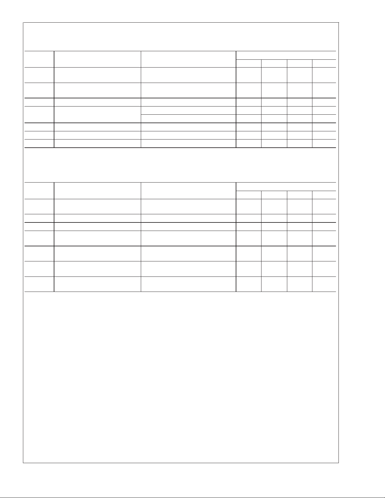
Electrical Characteristics for LM4652 (Notes 1, 2, 7) (Continued)
LM4651 & LM4652
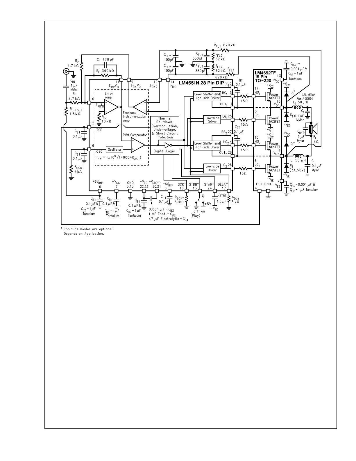
FIGURE 1. Typical Application Circuit and Test Circuit
DS101277-68
www.national.com 4
Page 5
LM4651 Pin Descriptions
Pin No. Symbol Description
1 OUT
2,27 BS
3HG
4HG
1
,BS
1
2
1
2
5,15 GND The ground pin for all analog circuitry.
6 +6V
7+V
8 −6V
9F
10 E
11 E
BYP
CC
BYP
BKVO
RRIN
RRVO
12 TSD The thermal shut down input pin for the thermal shut down output of the LM4652.
13 STBY Standby function input pin. This pin is CMOS compatible.
14 FBK
1
16 OSC
17 Delay The dead time setting pin.
18 SCKT Short circuit setting pin. Minimum setting is 10A.
19 FBK
20,21 −V
22,23 −V
2
DDBYP
EE
24 START
25 LG
26 LG
28 OUT
1
2
2
The reference pin of the power MOSFET output to the gate drive circuitry.
The bootstrap pin provides extra bias to drive the upper gates, HG1,HG2.
High−Gate#1 is the gate drive to a top side MOSFET in the H-Bridge.
High−Gate#2 is the gate drive to a top side MOSFET in the H-Bridge.
The internally regulated positive voltage output for analog circuitry. This pin is available
for internal regulator bypassing only.
The positive supply input for the IC.
The internally regulated negative voltage output for analog circuitry. This pin is available
for internal regulator bypassing only.
The feedback instrumentation amplifier output pin.
The error amplifier inverting input pin. The input audio signal and the feedback signal are
summed at this input pin.
The error amplifier output pin.
The feedback instrumentation amplifier pin. This must be connected to the feedback filter
from V
(pin 15 on the LM4652 ).
O1
The switching frequency oscillation pin. Adjusting the resistor from 15.5kΩ to 0Ω
changes the switching frequency from 75kHz to 225kHz.
The feedback instrumentation amplifier pin. This must be connected to the feedback filter
from V
(pin 7 on the LM4652 ).
O2
The regulator output for digital blocks. This pin is for bypassing only.
The negative voltage supply pin for the IC.
The start up capacitor input pin. This capacitor adjusts the start up time of the diagnostic
sequence for the modulator. Refer to Start up Sequence and Timing in the
Application Information section.
Low−Gate#1 is the gate drive to a bottom side MOSFET in the H-Bridge.
Low−Gate#2 is the gate drive to a bottom side MOSFET in the H-Bridge.
The reference pin of the power MOSFET output to the gate drive circuitry.
LM4651 & LM4652
www.national.com5
Page 6
LM4652 Pin Descriptions
Pin No. Symbol Description
1 GND A ground reference for the thermal shut down circuitry.
LM4651 & LM4652
2LG
3−V
1
EE
4 TSD
Low−Gate#1 is the gate input to a bottom side MOSFET in the H-Bridge.
The negative voltage supply input for the power MOSFET H-Bridge.
The thermal shut down flag pin. This pin transitions to 6V when the die temperature
exceeds 150˚C.
5 NC No connection
6LG
7VO
2
2
Low−Gate#2 is the gate input to a bottom side MOSFET in the H-Bridge.
The switching output pin for one side of the H-Bridge.
8 NC No connection.
9 NC No connection.
10 HG
2
High−Gate#2 is the gate input to a top side MOSFET in the H-Bridge.
11 NC No connection.
12 NC No connection.
13 +V
14 HG
15 VO
CC
1
2
The positive voltage supply input for the power MOSFET H-Bridge.
High−Gate#1 is the gate input to a top side MOSFET in the H-Bridge.
The switching output pin for one side of the H-Bridge.
Note: NC, no connect pins are floating pins. It is best to connect the pins to GND to minimize any noise from being coupled into
the pins.
External Components Description (Refer to Figure 1)
Components Functional Description
1. R
2. R
3. R
4. C
1
2
f
f
Works with R2,R
)/ R
R
)−(R2/R1) + .5].
fl2
fl2
See description above for R1.
Sets the gain and bandwidth of the system by creating a low pass filter for the Error
Amplifier’s feedback with C
See description above for Rf.
fl1
and R
to set the gain of the system. Gain = [(R2/R1) x ((R
fl2
. 3dB pole is at fC= 1/(2πRfCf) (Hz).
f
Provides a reduction in the feedback with R
5. R
fI1
reduce effects on the pole created by R
fI2
System Gain.
6. R
7. C
8. R
9. C
10. L
11. C
12. C
byp
and C
fI2
fI1
fI3
fI2
1
1
fI2
note for R
See description above for R
Establish the second pole for the low pass filter in the feedback path at fC=
1/(2πR
See description above for R
Combined with C
= 1/[2π(L12C
Filters high frequency noise from the amplifier’s output to ground. Recommended value
is 0.1µF to 1µF.
See description for L1.
creates a low pass filter with a pole at fC= 1/(2πR
fI1
for effect on System Gain.
1,R2
.
fI2
) (Hz).
fI3CfI2
.
fI3
creates a 2−pole, low pass output filter that has a −3dB pole at f
BYP
1
)
⁄
2
] (Hz).
BYP
R
Bypass capacitors for VCC,VEE, analog and digital voltages (VDD, +6V, −6V). See
13. C
B1−CB4
Supply Bypassing and High Frequency PCB Design in the Application Information
section for more information.
14. B
15. R
16. C
START
17. R
18. R
19. D
BT
DLY
SCKT
OSC
1
Provides the bootstrap capacitance for the boot strap pin.
Sets the dead time or break before make to T
Controls the startup time with T
Sets the output short circuit current with I
START
= (8.5x10⁴)C
SCKT
Controls the switching frequency with fSW=1X10⁹/ (4000 + R
Schottky diode to protect the output MOSFETs from fly back voltages.
should be 10 X R
fI2.RfI1
and C
. See also note for R1,R2for effect on
fI1
= (1.7x10
DLY
START
= (1x10⁵)/ (10kΩ\ R
fI2CfI1
−12
)(500+R
(seconds).
OSC
minimum to
fI2
) (Hz). See also
) (seconds).
DLY
) (A).
SCKT
) (Hz).
+
fl1
C
www.national.com 6
Page 7

External Components Description (Refer to Figure 1) (Continued)
Components Functional Description
,
C
20.
21. R
SBY1,CSBY2
C
OFFSET
22. C
23. R
SBY3
IN
gate
Supply de-coupling capacitors. See Supply Bypassing in the Application Information
section.
Provides a small DC voltage at the input to minimize the output DC offset seen by the
load. This also minimize power on pops and clicks.
Blocks DC voltages from being coupled into the input and blocks the DC voltage created
OFFSET
from the source.
by R
Slows the rise and fall time of the gate drive voltages that drive the output FET’s.
Typical Performance Characteristics
LM4651 & LM4652
Output Power vs. Supply Voltage
THD+N vs. Output Power
R
=4Ω
L
DS101277-4
Output Power vs. Supply Voltage
THD+N vs. Output Power
R
=8Ω
L
DS101277-5
DS101277-6
DS101277-7
www.national.com7
Page 8

Typical Performance Characteristics (Continued)
THD+N vs. Output Power
R
=4Ω
L
LM4651 & LM4652
THD+N vs. Frequency vs. Bandwidth
R
=4Ω
L
DS101277-8
THD+N vs. Output Power
R
=8Ω
L
THD+N vs. Frequency vs. Bandwidth
R
=8Ω
L
DS101277-9
DS101277-10
THD+N vs. Frequency vs. Bandwidth
R
=4Ω
L
DS101277-12
www.national.com 8
THD+N vs. Frequency vs. Bandwidth
R
=8Ω
L
DS101277-11
DS101277-13
Page 9

Typical Performance Characteristics (Continued)
LM4651 & LM4652
Power Dissipation & Efficiency
vs. Output Power
Frequency Response
R
=4Ω
L
DS101277-16
Clipping Power Point & Efficiency
vs. Switching Frequency (f
SW
)
Supply Current vs. Switching Frequency
(LM4651 & LM4652)
DS101277-17
Supply Current vs. Supply Voltage
(LM4651 & LM4652)
DS101277-18
DS101277-21
R
DS
(ON)
DS101277-20
vs. Temperature
DS101277-23
www.national.com9
Page 10

Application Information
GENERAL FEATURES
System Functional Information: The LM4651 is a conven-
tional pulse width modulator/driver. As Figure 2 shows the
incoming audio signal is compared with a triangle waveform
with a much higher frequency than the audio signal (not
LM4651 & LM4652
drawn to scale). The comparator creates a variable duty
cycle squarewave. The squarewave has a duty cycle proportional to the audio signal level. The squarewave is then
properly conditioned to drive the gates of power MOSFETs in
an H-bridge configuration, such as the LM4652. The pulse
train of the power MOSFETs are then fed into a low pass
filter (usually a LC) which removes the high frequency and
delivers an amplified replica of the audio input signal to the
load.
DS101277-1
FIGURE 2. Conventional Pulse Width Modulation
Standby Function: The standby function of the LM4651 is
CMOS compatible, allowing the user to perform a muting of
the music as well as turning off all power MOSFETs by
shutting down the pulse width waveform. Standby has the
added advantage of minimizing the quiescent current. Because standby shuts down the pulse width waveform, the
attenuation of the music is complete (
mized, and any output noise is eliminated since there is no
modulation waveform. By placing a logic ’1’ or 5V at pin 13,
the standby function will be enabled. A logic ’0’ or 0V at pin
13 will disable the standby function allowing modulation by
the input signal.
>
120dB), EMI is mini-
The value of C
sets the time it takes for the IC to go
START
though the start-up sequence and the frequency that the
diagnostic circuitry checks to see if an error condition has
been corrected. An Error condition occurs if current limit,
thermal shut down, under voltage detection, or standby are
sensed. The self-diagnostic circuit checks to see if any one
of these error flags has been removed at a frequency set by
the C
capacitor. For example, if the value of C
START
START
10µF then the diagnostic circuitry will check approximately
every second to see if an error condition has been corrected.
If the error condition is no longer present, the LM4651/52 will
return to normal operation.
DS101277-70
FIGURE 3. Startup Timing Diagram
Current Limiting and Short Circuit Protection: The resis-
tor value connected between the SCKT pin and GND determines the maximum output current. Once the output current
is higher than the set limit, the short circuit protection turns
all power MOSFETsoff. The current limit is set to a minimum
of 10A internally but can be increased by adjusting the value
of the R
resistor.Equation (3) shows how to find R
SCKT
I
= 1X10⁵/(10kΩ\ R
SCKT
) (Amps) (3)
SCKT
SCKT
is
.
Under Voltage Protection: The under voltage protection
disables the output driver section of the LM4651 while the
supply voltage is below
±
10.5V. This condition can occur as
power is first applied or when low line, changes in load
resistance or power supply sag occurs. The under voltage
protection ensures that all power MOSFETs are off, eliminating any shoot-through current and minimizing pops or clicks
during turn-on and turn-off. The under voltage protection
gives the digital logic time to stabilize into known states
providing a popless turn on.
Start Up Sequence and Self-Diagnostic Timing: The
LM4651 has an internal soft start feature (see Figure 3) that
ensures reliable and consistent start-up while minimizing
turn-on thumps or pops. During the start-up cycle the system
is in standby mode. This start-up time is controlled externally
by adjusting the capacitance (C
) value connected to
START
the START pin. The start-up time can be controlled by the
capacitor value connected to the START pin given by Equation (1) or (2):
t
= (8.4x10⁴)C
START
C
START=TSTART
www.national.com 10
START
/(8.5x104) (Farads) (2)
(seconds) (1)
This feature is designed to protect the MOSFETs by setting
the maximum output current limit under short circuit conditions. It is designed to be a fail-safe protection when the
output terminals are shorted or a speaker fails and causes a
short circuit condition.
Thermal Protection The LM4651 has internal circuitry (pin
12) that is activated by the thermal shutdown output signal
from the LM4652 (pin 4). The LM4652 has thermal shut
down circuitry that monitors the temperature of the die. The
voltage on the TSD pin (pin 4 of the LM4652) goes high (6V)
once the temperature of the LM4652 die reaches 150˚C.
This pin should be connected directly to the TSD pin of the
LM4651 (pin 12). The LM4651 disables the pulse width
waveform when the LM4652 transmits the thermal shutdown
flag. The pulse width waveform remains disabled until the
TSD flag from the LM4652 goes low, signaling the junction
temperature has cooled to a safe level.
Dead Time Setting The DELAY pin on the LM4651 allows
the user to set the amount of dead time or break before
make of the system. This is the amount of time one pair of
FETs are off before another pair is switched on. Increased
dead time will reduce the shoot through current but has the
disadvantage of increasing THD. The dead time should be
Page 11

Application Information (Continued)
reduced as the desired bandwidth of operation increases.
The dead time can be adjusted with the R
Equation (4):
T
DLY
= 1.7x10
−12
(500 + R
) (Seconds) (4)
DLY
Currently, the recommended value is 5kΩ.
Oscillator Control: The modulation frequency is set by an
external resistor, R
, connected between pin 16 and
OSC
GND. The modulation frequency can be set within the range
of 50kHz to 225kHz according to the design requirements.
The values of R
OSC
and f
can be found by Equation (5)
OSC
and (6):
f
= 1x10⁹/ (4000 + R
OSC
R
= (1x10⁹/f
OSC
) − 4000 (Ω) (6)
OSC
) (Hz) (5)
OSC
DLY
resistor by
LM4651 & LM4652
Feedback Amplifier and Filter: The purpose of the feed-
back amplifier is to differentially sample the output and provide a single-ended feedback signal to the error amplifier to
close the feedback loop. The feedback is taken directly from
the switching output before the demodulating LC filter to
avoid the phase shift caused by the output filter. The signal
fed back is first low pass filtered with a single pole or dual
pole RC filter to remove the switching frequency and its
harmonics. The differential signal, derived from the bridge
output, goes into the high input impedance instrumentation
amplifier that is used as the feedback amplifier. The instrumentation amplifier has an internally fixed gain of 1. The use
of an instrumentation amplifier serves two purposes. First,
it’s input are high impedance so it doesn’t load down the
output stage. Secondly, an IA has excellent common-mode
rejection when its gain setting resistors are properly
matched. This feature allows the IA to derive the true feedback signal from the differential output, which aids in improving the system performance.
Equations (5) and (6) are for R
greater than zero will increase the value needed for R
For R
DLY
=5kΩ,R
will need to be increased by about
OSC
= 0. Using a value of R
DLY
DLY
OSC
2kΩ.As the graphs show, increasing the switching frequency
will reduce the THD but also decreases the efficiency and
maximum output power level before clipping. Increasing the
switching frequency increases the amount of loss because
switching currents lower the efficiency across the output
power range. A higher switching frequency also lowers the
maximum output power before clipping or the 1% THD point
occur.
Over-Modulation Protection: The over-modulation protection is an internally generated fixed pulse width signal that
prevents any side of the H-bridge power MOSFETs from
remaining active for an extended period of time. This condition can result when the input signal amplitude is higher than
the internal triangle waveform. Lack of an over modulation
signal can increase distortion when the amplifier’s output is
clipping. Figure 4 shows how the over modulation protection
works.
DS101277-2
FIGURE 4. Over Modulation Protection
The over modulation protection also provides a ’soft clip’
type response on the top of a sine wave. This minimum
pulse time is internally set and cannot be adjusted. As the
switching frequency increases this minimum time becomes a
higher percentage of the period (T
= 1/fSW). Because
PERIOD
the over modulation protection time is a higher percentage of
the period, the peak output voltage is lower and, therefore,
the output power at clipping is lower for the same given
supply rails and load.
.
DS101277-3
FIGURE 5. Feedback instrumentation Amplifier
Schematic
Error Amplifier: The purpose of the error amplifier is to sum
the input audio signal with the feedback signal derived from
the output. This inverting amplifier’s gain is externally configurable by resistors Rf and R1. The parallel feedback capacitor and resistor form a low pass filter that limits the
frequency content of the input audio signal and the feedback
signal. The pole of the filter is set by Equation (7).
f
= 1/(2πRfCf) (Hz) (7)
IP
On-Board Regulators: The LM4651 has its own internal
supply regulators for both analog and digital circuits. Sepa-
±
rate
6V regulators exist solely for the analog amplifiers,
oscillator and PWM comparators. A separate voltage regulator powers the digital logic that controls the protection,
level shifting, and high−/low−side driver circuits. System performance is enhanced by bypassing each regulator’s output.
±
The
6V regulator outputs, labeled +6V
−6V
regulator output, −V
passed to −V
(pin 8) should be bypassed to ground. The digital
BYP
DDBYP
(pins 22 & 23). The voltage level of −V
EE
(pins 20 & 21) should be by-
(pin 6) and
BYP
DDBYP
should be always be 6V closer to ground than the negative
rail, −V
. As an example, if −VEE= −20V, then −V
EE
DDBYP
should equal −14V. Recommended capacitor values and
type can be found in Figure 1, Typical audio Application
Circuit.
APPLICATIONS HINTS
www.national.com11
Page 12

Application Information (Continued)
Introduction
National Semiconductor (NSC) is committed to providing
application information that assists our customers in obtaining the best performance possible from our products. The
LM4651 & LM4652
following information is provided in order to support this
commitment. The reader should be aware that the optimization of performance was done using a reference PCB designed by NSC and shown in Figure 7 through 11. Variations
in performance can occur because of physical changes in
the printed circuit board and the application. Therefore, the
designer should know that component value changes may
be required in order to optimize performance in a given
application. The values shown in this data sheet can be used
as a starting point for evaluation purposes. When working
with high frequency circuits, good layout practices are also
critical to achieving maximum performance.
pin(s) using leads as short as possible. For supply stabilizing, large electrolytic capacitors (3,300µF to 15,000µF) are
needed. The value used is design and cost dependent.
High Frequency PCB Design
A double-sided PCB is recommended when designing a
class D amplifier system. One side should contain a ground
plane with the power traces on the other side directly over
the ground plane. The advantage is the parasitic capacitance created between the ground plane and the power
planes. This parasitic capacitance is very small (pF) but is
the value needed for coupling high frequency noise to
ground. At high frequencies, capacitors begin to act more
like inductors because of lead and parasitic inductance in the
capacitor. For this reason, bypassing capacitors should be
surface mount because of their low parasitic inductance.
Equation (8) shows how to determine the amount of power to
ground plane capacitance.
Input Pre-Amplifier with Subwoofer Filter
The LM4651 and LM4652 Class D solution is designed for
low frequency audio applications where low gain is required.
This necessitates a pre−amplifier stage with gain and a low
pass audio filter. An inexpensive input stage can be designed using National’s LM833 audio operational amplifier
and a minimum number of external components. Again of 10
(20dB) is recommended for the pre−amplifier stage. For a
subwoofer application, the pole of the low pass filter is
normally set within the range of 60Hz − 180Hz. For a clean
sounding subwoofer the filter should be at least a
second-order filter to sharply roll off the high frequency audio
signals.A higher order filter is recommended for stand-alone
self-powered subwoofer applications. Figure 6 shows a
simple input stage with a gain of 10 and a second-order low
pass filter.
DS101277-77
FIGURE 6. Pre−amplifier Stage with Low Pass Filter
C=eoerA/d (Farads) (8)
where eo = 0.22479pF/in and er = 4.1
A is the common PCB area and d is the distance between
the planes. The designer should target a value of 100pF or
greater for both the positive supply to ground capacitance
and negative supply to ground capacitance. Signal traces
that cross over each other should be laid out at 90˚ to
minimized any coupling.
Output Offset Voltage Minimization
The amount of DC offset voltage seen at the output with no
input signal present is already quite good with the LM4651/
52. With no input signal present the system should be at
50% duty cycle.Any deviation from 50% duty cycle creates a
DC offset voltage seen by the load. To completely eliminate
the DC offset, a DC voltage divider can be used at the input
to set the DC offset to near zero. This is accomplished by a
simple resistor divider that applies a small DC voltage to the
input. This forces the duty cycle to 50% when there is no
input signal. The result is a LM4651 and LM4652 system
with near zero DC offset. The divider should be a 1.8MΩ
from the +6V output (pin 6) to the input (other side of 25k,
R
). R1acts like the second resistor in the divider. Also use
1
a 1µF input capacitor before R
the source. R
and the 1µF capacitor create a high pass filter
1
with a 3dB point at 6.35Hz. The value of R
to block the DC voltage from
1
is set
OFFSET
according to the application. Variations in switching frequency and supply voltage will change the amount of offset
voltage requiring a different value than stated above. The
value above (1.8MΩ)isfor
±
20V and a switching frequency
of 125kHz.
Supply Bypassing
Correct supply bypassing has two important goals. The first
is to ensure that noise on the supply lines does not enter the
circuit and become audible in the output. The second is to
help stabilize an unregulated power supply and provide current under heavy current conditions. Because of the two
different goals multiple capacitors of various types and values are recommended for supply bypassing. For noise
de-coupling, generally small ceramic capacitors (.001µF to
.1µF) along with slightly larger tantalum or electrolytic capacitors (1µF to 10µF) in parallel will do an adequate job of
removing most noise from the supply rails. These capacitors
should be placed as close as possible to each IC’s supply
www.national.com 12
Output Stage Filtering
As common with Class D amplifier design, there are many
trade-offs associated with different circuit values. The output
stage is not an exception. National has found good results
with a 50µF inductor and a 5µF Mylar capacitor (see Figure
1, Typical Audio Application Circuit) used as the output
LC filter. The two-pole filter contains three components; L
and C
output. The design formula for a bridge output filter is f
1/[2π(L
because the LM4651 and LM4652 have a bridged
BYP
1
)
⁄
2
12CBYP
].
C
A common mistake is to connect a large capacitor between
ground and each output. This applies only to single-ended
1
=
Page 13

Application Information (Continued)
applications. In bridge operation, each output sees C
This causes the extra factor of 2 in the formula. The alternative to C
V
, and V
O
size or cost efficient because each capacitor must be twice
C
BYP
is a capacitor connected between each output,
BYP
, and ground. This alternative is, however, not
O
2
’s value to achieve the same filter cutoff frequency. The
additional small value capacitors connected between each
output and ground (C
) help filter the high frequency from the
1
output to ground . The recommended value for C
1µF or 2% to 20% of C
BYP
.’
Modulation Frequency Optimization
Setting the modulation frequency depends largely on the
application requirements. To maximize efficiency and output
power a lower modulation frequency should be used. The
lower modulation frequency will lower the amount of loss
caused by switching the output MOSFETs increasing the
efficiency a few percent. A lower switching frequency will
also increase the peak output power before clipping because
the over modulation protection time is a smaller percentage
of the total period. Unfortunately, the lower modulation frequency has worse THD+N performance when the output
power is below 10 watts. The recommended switching frequency to balance the THD+N performance, efficiency and
output power is 125kHz to 145kHz.
THD+N Measurements and Out of Audio Band Noise
THD+N (Total Harmonic Distortion plus Noise) is a very
important parameter by which all audio amplifiers are measured. Often it is shown as a graph where either the output
power or frequency is changed over the operating range. A
very important variable in the measurement of THD+N is the
bandwidth limiting filter at the input of the test equipment.
Class D amplifiers, by design, switch their output power
devices at a much higher frequency than the accepted audio
range (20Hz - 20kHz). Switching the outputs makes the
amplifier much more efficient than a traditional Class A/B
amplifier. Switching the outputs at high frequency also increases the out-of-band noise. Under normal circumstances
this out-of-band noise is significantly reduced by the output
low pass filter. If the low pass filter is not optimized for a
given switching frequency, there can be significant increase
in out-of-band noise.
THD+N measurements can be significantly affected by
out-of-band noise, resulting in a higher than expected
THD+N measurement. To achieve a more accurate measurement of THD, the bandwidth at the input of the test
equipment must be limited. Some common upper filter points
are 22kHz, 30kHz, and 80kHz. The input filter limits the
noise component of the THD+N measurement to a smaller
bandwidth resulting in a more real-world THD+N value.
The output low pass filter does not remove all of the switching fundamental and harmonics. If the switching frequency
fundamental is in the measurement range of the test equipment, the THD+N measurement will include switching frequency energy not removed by the output filter.Whereas the
switching frequency energy is not audible, it’s presence degrades the THD+N measurement. Reducing the bandwidth
to 30kHz and 22kHz reveals the true THD performance of
is 0.1µF to
1
BYP
LM4651 & LM4652
the Class D amplifier. Increasing the switching frequency or
reducing the cutoff frequency of the output filter will also
.
reduce the level of the switching frequency fundamental and
it’s harmonics present at the output. This is caused by a
switching frequency that is higher than the output filter cutoff
frequency and, therefore, more attenuation of the switching
frequency.
In-band noise is higher in switching amplifiers than in linear
amplifiers because of increased noise from the switching
waveform. The majority of noise is out of band (as discussed
above), but there is also an increase of audible noise. The
output filter design (order and location of poles) has a large
effect on the audible noise level. Power supply voltage also
has an effect on noise level. The output filter removes a
certain amount of the switching noise. As the supply increases, the attenuation by the output fiter is constant. However, the switching waveform is now much larger resulting in
higher noise levels.
THERMAL CONSIDERATIONS
Heat Sinking
The choice of a heat sink for the output FETs in a Class D
audio amplifier is made such that the die temperature does
not exceed T
and activate the thermal protection cir-
JMAX
cuitry under normal operating conditions. The heat sink
should be chosen to dissipate the maximum IC power which
occurs at maximum output power for a given load. Knowing
the maximum output power, the ambient temperature surrounding the device, the load and the switching frequency,
the maximum power dissipation can be calculated. The additional parameters needed are the maximum junction temperature and the thermal resistance of the IC package (θ
JC
junction to case), both of which are provided in the Absolute
Maximum Ratings and Operating Ratings sections above.
It should be noted that the idea behind dissipating the power
within the IC is to provide the device with a low resistance to
convection heat transfer such as a heat sink. Convection
cooling heat sinks are available commercially and their
manufacturers should be consulted for ratings. It is always
safer to be conservative in thermal design.
Proper IC mounting is required to minimize the thermal drop
between the package and the heat sink. The heat sink must
also have enough metal under the package to conduct heat
from the center of the package bottom to the fins without
excessive temperature drop. A thermal grease such as
Wakefield type 120 or Thermalloy Thermacote should be
used when mounting the package to the heat sink. Without
some thermal grease, the thermal resistance θ
CS
(case to
sink) will be no better than 0.5˚C/W, and probably much
worse. With the thermal grease, the thermal resistance will
be 0.2˚C/W or less. It is important to properly torque the
mounting screw. Over tightening the mounting screw will
cause the package to warp and reduce the contact area with
the heat sink. It can also crack the die and cause failure of
the IC. The recommended maximum torque applied to the
mounting screw is 40 inch-lbs. or 3.3 foot-lbs.
Determining Maximum Power Dissipation
Power dissipation within the integrated circuit package is a
very important parameter. An incorrect maximum power dissipation (P
) calculation may result in inadequate heat sink-
D
ing, causing thermal shutdown circuitry to operate intermittently. There are two components of power dissipation in a
class D amplifier. One component of power dissipation in the
,
www.national.com13
Page 14

Application Information (Continued)
LM4652 is the R
current when operating at maximum output power.The other
component of power dissipation in the LM4652 is the switching loss. If the output power is high enough and the DC
resistance of the filter coils is not minimized then significant
loss can occur in the output filter. This will not affect the
LM4651 & LM4652
power dissipation in the LM4652 but should be checked to
be sure that the filter coils with not over heat.
The first step in determining the maximum power dissipation
is finding the maximum output power with a given voltage
and load. Refer to the graph Output Power verses Supply
Voltagetodetermine the output power for the given load and
supply voltage. From this power, the RMS output current can
be calculated as I
dissipation caused by the output current is P
(I
OUTRMS
2
)
*
(2*R
found from the Electrical Characteristics for the LM4652
table above. The percentage of loss due to the switching is
calculated by Equation (9):
%LOSS
SWITCH
t
and T
r,tf
OVERMOD
teristic for the LM4651 and Electrical Characteristic for
the LM4652 sections above. The system designer deter-
mines the value for f
pation caused by switching loss is found by Equation (10).
P
OUTMAX
is the 1% output power for the given supply voltage
and the load impedance being used in the application. P
can be determined from the graph Output Power vs.
MAX
Supply Voltage in the Typical Performance Characteristics section above.
P
DSWITCH
(1−%LOSS
P
for the LM4652 is found by adding the two compo-
DMAX
nents (P
DSWITCH
Determining the Correct Heat Sink
Once the LM4652’s power dissipation known, the maximum
thermal resistance (in ˚C/W) of a heat sink can be calculated.
This calculation is made using Equation (11) and is based on
the fact that thermal heat flow parameters are analogous to
electrical current flow properties.
P
=(T
DMAX
JMAX−TAMBIENTMAX
Where θ
Since we know θJC, θCS, and T
Maximum Ratings and Operating Ratings sections above
(taking care to use the correct θ
on which package type is being used in the application) and
have calculated P
the heat sink’s thermal resistance. The following equation is
derived from Equation (11):
θ
= [(T
SA
JMAX−TAMBIENTMAX
of the FET times the RMS output
DS
(ON)
OUTRMS
= SQRT(P
). The value for R
DS
(ON)
=(tr+tf+T
OVERMOD
OUT/RL
)*f
SW
can be found in the Electrical Charac-
(switching frequency). Power dissi-
SW
= (%LOSS
+P
DOUT
SWITCH
) of power dissipation together.
*
SWITCH
P
OUTMAX
) (Watts) (10)
)/θJA(Watts) (11)
= θJC+ θCS+ θ
DMAX
JA
and T
JMAX
for the LM4652 depending
JC
AMBIENTMAX
SA
from the Absolute
, we only need θSA,
)/P
DMAX
). The power
DOUT
can be
DS
(ON)
(9)
OUT
)/
]−θJC− θ
CS
Again, it must be noted that the value of θSAis dependent
upon the system designer’s application and its corresponding parameters as described previously. If the ambient temperature surrounding the audio amplifier is higher than
T
AMBIENTMAX
, then the thermal resistance for the heat sink,
given all other parameters are equal, will need to be lower.
Example Design of a Class D Amplifier
The following is an example of how to design a class D
amplifier system for a power subwoofer application utilizing
the LM4651 and LM4652 to meet the design requirements
listed below:
Output Power, 1% THD 125W
•
Load Impedance 4Ω
=
•
Input Signal level 3V RMS (max)
•
Input Signal Bandwidth 10Hz − 150Hz
•
Ambient Temperature 50˚C (max)
•
Determine the Supply Voltage
From the graph Output Power verses Supply voltage at
1% THD the supply voltage needed for a 125 watt, 4Ω
application is found to be
Determine the Value for R
±
20V.
(Modulation Frequency)
OSC
The oscillation frequency is chosen to obtain a satisfactory
efficiency level while also maintaining a reasonable THD
-
performance. The modulation frequency can be chosen using the Clipping Power Point and Efficiency verses
Switching Frequency graph. A modulation frequency of
125kHz is found to be a good middle ground for THD performance and efficiency.The value of the resistor for R
OSC
is
found from Equation (6) to be 3.9 kΩ.
Determine the Value for R
(Circuit Limit)
SCKT
The current limit is internally set as a failsafe to 10 amps.
The inductor ripple current and the peak output current must
be lower than 10 amps or current limit protection will turn on.
Atypical 4Ω load driven by a filter using 50µH inductors does
not require more than 10A. The current limit will have to be
increased when loads less than 4Ω are used to acheive
higher output power. With R
equal to 100kΩ, the current
SCKT
limit is 10A.
Determine the Value for R
(Dead Time Control)
DLY
The delay time or dead time is set to the recommended
value so R
is desired, R
value for R
equals 5kΩ. If a higher bandwidth of operation
DLY
should be a lower value resistor. If a zero
DLY
is desired, connect the LM4651’s pin 17 to
DLY
GND.
Determine the Value of L
C
(the Output and Feedback Filters)
f
1,CBYP,C1,Rfl1Rfl2,Cfl1Cfl2,Rf
All component values show in
Figure 1
Typical Audio Ap-
,
plication Circuit, are optimized for a subwoofer application.
Use the following guidelines when changing any component
values from those shown. The frequency response of the
output filter is controlled by L
and C
1
. Refer to the Ap-
BYP
plication Information section titled Output Stage Filtering
for a detailed explanation on calculating the correct values
for L
and C
1
BYP
.
www.national.com 14
Page 15

Application Information (Continued)
C
should be in the range of 0.1µF to 1µF or 2 - 20% of C
1
R
fl1
and R
are found by the ratio R
fl2
fl1
= 10R
fl2
Alower ratio can be used if the application is for lower output
voltages than the 125Watt, 4Ω solution show here.
The feedback RC filter’s pole location should be higher than
the output filter pole. The reason for two capacitors in parallel instead of one larger capacitor is to reduce the possible
EMI from the feedback traces. C
is placed close as pos-
fl1
sible to the output of the LM4652 so that an audio signal is
present on the feedback trace instead of a high frequency
square wave. C
is then placed as close as possible to the
fl2
feedback inputs (pins 14, 19) of the LM4651 to filter off any
noise picked up by the feedback traces. The combination
lowers EMI and provides a cleaner audio feedback signal to
the LM4651. R
should be in range of 100kΩ to1MΩ.C
f
controls the bandwidth of the error signal and should be in
the range of 100pF to 470pF.
BYP
.
LM4651 & LM4652
Equations (9) - (11) to calculate the amount of power dissi-
.
f
pation for the LM4652. The appropriate heat sink size, or
thermal resistance in ˚C/W, will then be determined.
Equation (9) determines the percentage of loss caused by
the switching. Use the typical values given in the Electrical
Characteristics for the LM4651 and Electrical Characteristics for the LM4652 tables for the rise time, fall time and
over modulation time:
*
%Loss = (25ns+26ns+350ns)
125kHz
%Loss = 5.0%
This switching loss causes a maximum power dissipation,
using Equation (10), of:
P
DSWITCH
= (5.0%*125W) / (1−5.0%)
P
DSWITCH
= 6.6W
Determine the Value for C
(Start Up Delay)
START
The start-up delay is chosen to be 1 second to ensure
minimum pops or clicks when the amplifier is powered up.
Using Equation (2), the value of C
is 11.7µF.Astandard
START
value of 10µF is used.
Determine the Value of Gain, R
, and R
1
2
The gain is set to produce a 125W output at no more than
1% distortion with a 3V
4Ω load requires a 22.4V
input. A dissipation of 125W in a
RMS
signal. To produce this output
RMS
signal, the LM4651/LM4652 amplifier needs an overall
closed-loop gain of 22.4V
RMS
/3V
, or 7.5V/V (17.5db).
RMS
Equation (12) shows all the variables that affect the system
gain.
Gain = [(R
The values for R
the Value of the Filters section above. Therefore, R
620kΩ,R
fI2
also found as the first step in this example to be
2/R1
fI1,RfI2
) x ((R
fl1+Rfl2
, and Rfwere found in the Determine
)/ R
)−(R2/R1) + .5].(3)
fl2
fI1
= 62kΩ and Rf= 390kΩ. The value of VCCwas
±
20V.
Inserting these values into equation (12) and reducing gives
the equation below:
R
= .7R
2
1
The input resistance is desired to be 20kΩ so R
20kΩ.R
Lowering R
ing R
is then found to be 14kΩ.
2
direcly affects the noise of the system. Chang-
2
to increase gain with the lower value for R2has very
1
is set to
1
(4)
little affect on the noise level. The percent change in noise is
about what whould be expected with a higher gain. The
drawback to a lower R
value is a larger CINvalue, neces-
1
sary to properly couple the lowest desired signal frequencies. If a 20kΩ input impedance is not required, then the
recommended values shown in
Application Circuit should be used: with R
4.7kΩ and R
’s value set to 3.5kΩ for a gain 7.5V/V.
2
Figure 1
, Typical Audio
’s value set to
1
Determine the Needed Heat Sink
The only remaining design requirement is a thermal design
that prevents activating the thermal protection circuitry. Use
Next the power dissipation caused by the R
DS(ON)
of the
output FETs is found by multiplying the output current times
the R
. Again, the value for R
DS(ON)
is found from the
DS(ON)
Electrical Characteristics for the LM4652 table above.
The value for R
at 100˚C is used since we are calcu-
DS(ON)
lating the maximum power dissipation.
I
OUTRMS
= SQRT(125watts/4Ω) = 5.59 amps
2
P
RDS(ON)
= (5.59A)
P
RDS(ON)
*
(0.230Ω*2)
= 14.4W
The total power dissipation in the LM4652 is the sum of
these two power losses giving:
P
= 6.6W + 14.4W = 21W
DTOTAL
The value for Maximum Power Dissipation given in the Sys-
tem Electrical Characteristics for the LM4651 and
=
LM4652 is 22 watts. The difference is due to approximately
1 watt of power loss in the LM4651. The above calculations
are for the power loss in the LM4652.
Lastly,use Equation (11) to determine the thermal resistance
of the LM4652’s heat sink. The values for θ
JC
and T
JMAX
are
found in the Operating Ratings and the Absolute Maxi-
mum Ratings section above for the LM4652. The value of
θ
is 2˚C/W for the isolated (TF) package or 1˚C/W for the
JC
non-isolated (T) package. The value for T
value for θ
is set to 0.2˚C/W since this is a reasonable
CS
is 150˚C. The
JMAX
value when thermal grease is used. The maximum ambient
temperature from the design requirements is 50˚. The value
of θ
for the isolated (TF) package is:
SA
θ
= [(150˚C − 50˚C)/21W] − 2˚C/W − 0.2˚C/W
SA
θ
= 2.5˚C/W
SA
and for the non-isolated (T) package without a mica washer
to isolate the heat sink from the package:
θ
= [(150˚C − 50˚C)/21W] − 1˚C/W − 0.2˚C/W
SA
θ
= 3.5˚C/W
SA
www.national.com15
Page 16
Application Information (Continued)
To account for the use of a mica washer simply subtract the
thermal resistance of the mica washer from θ
calculated
SA
above.
Recommendations for Critical External Components
LM4651 & LM4652
Circuit
Symbol
C
fI1
C
fI2
C
C
B2
C
B1&CBT
C
B3
C
1&CBYP
C
1&CBYP
D
L
L
L
f
1
1
1
1
Suggested
Value
Suggested Type Supplier/Contact Information
330pF Ceramic Disc
100pF Ceramic Disc
470pF Ceramic Disc
1µF Resin Dipped Solid Tantalum
0.1µF Monolithic Ceramic
0.001µF Monolithic Ceramic
5µF - 10µF Metalized Polypropylene or
Polyester Film
5µF - 10µF Metalized Polypropylene or
Polyester Film
3A, 50V Fast Schottky Diode
47µH, 5A High Saturation Open Core
(Vertical Mount Power Chokes)
50µH, 5.6A High Saturation Flux Density
Ferrite Rod
68µH, 7.3A High Saturation Flux Density
Ferrite Rod
Bishop Electronics Corp.
(562) 695 - 0446
http://www.bishopelectronics.com/
Nichicon Corp.
(847) 843-7500
http://www.nichicon-us.com/
CoilCraft
(847) 639-6400
http://www.coilcraft.com/
J.W. Miller
(310) 515-1720
http://www.jwmiller.com/
J.W. Miller
(310) 515-1720
http://www.jwmiller.com/
Supplier Part
#
BEC-9950
A11A-50V
QAF2Exx
or
QAS2Exx
PCV-0-
473-05
5504
5512
FIGURE 7. Reference PCB silkscreen layer
www.national.com 16
DS101277-29
Page 17

Application Information (Continued)
FIGURE 8. Reference PCB top layer
LM4651 & LM4652
DS101277-26
FIGURE 9. Reference PCB bottom layer
DS101277-27
www.national.com17
Page 18
Application Information (Continued)
LM4651 & LM4652
FIGURE 10. Reference PCB top layer solder mask
DS101277-28
FIGURE 11. Reference PCB bottom layer solder mask
www.national.com 18
DS101277-78
Page 19

Physical Dimensions inches (millimeters) unless otherwise noted
Order Number LM4651N
NS Package Number N28B
LM4651 & LM4652
Order Number LM4652TF
NS Package Number TF15B
www.national.com19
Page 20

Notes
170W Class D Audio Power Amplifier Solution
™
LIFE SUPPORT POLICY
NATIONAL’S PRODUCTS ARE NOT AUTHORIZED FOR USE AS CRITICAL COMPONENTS IN LIFE SUPPORT
DEVICES OR SYSTEMS WITHOUT THE EXPRESS WRITTEN APPROVAL OF THE PRESIDENT AND GENERAL
COUNSEL OF NATIONAL SEMICONDUCTOR CORPORATION. As used herein:
LM4651 & LM4652 Overture
1. Life support devices or systems are devices or
systems which, (a) are intended for surgical implant
into the body, or (b) support or sustain life, and
whose failure to perform when properly used in
accordance with instructions for use provided in the
labeling, can be reasonably expected to result in a
significant injury to the user.
2. A critical component is any component of a life
support device or system whose failure to perform
can be reasonably expected to cause the failure of
the life support device or system, or to affect its
safety or effectiveness.
National Semiconductor
Corporation
Americas
Tel: 1-800-272-9959
Fax: 1-800-737-7018
Email: support@nsc.com
www.national.com
National does not assume any responsibility for use of any circuitry described, no circuit patent licenses are implied and National reserves the right at any time without notice to change said circuitry and specifications.
National Semiconductor
Europe
Fax: +49 (0) 180-530 85 86
Email: europe.support@nsc.com
Deutsch Tel: +49 (0) 69 9508 6208
English Tel: +44 (0) 870 24 0 2171
Français Tel: +33 (0) 1 41 91 8790
National Semiconductor
Asia Pacific Customer
Response Group
Tel: 65-2544466
Fax: 65-2504466
Email: ap.support@nsc.com
National Semiconductor
Japan Ltd.
Tel: 81-3-5639-7560
Fax: 81-3-5639-7507
 Loading...