

Page 1
February 1999
LM4549
AC ’97 Rev 2.1 Codec with Sample Rate Conversion and
National 3D Sound
LM4549 AC ’97 Rev 2.1 Codec with Sample Rate Conversion and National 3D Sound
General Description
The LM4549 is an audio codec for PC systems which is fully
PC98 compliant and performs the analog intensivefunctions
of the AC97 Rev2.1 architecture. Using 18-bit Sigma-Delta
A/D’s and D/A’s, the LM4549 provides 90dB of Dynamic
Range.
The LM4549 was designed specifically to provide a high
quality audiopathand provide all analog functionality in a PC
audio system. It features full duplex stereo A/D’s and D/A’s
and an analog mixer with 4 stereo and 3 mono inputs, each
of which has separate gain, attenuation and mute control.
The codec features a second Line Output known as True
Line Level Out that is identical to Line Out but with independent volume control. The LM4549 also features National’s
3D Sound stereo enhancement and variable sample rate
conversion. The sample rate for the A/D and D/A can be programmed separately with a resolution of 1Hz to convert any
rate between 4kHz-48kHz.
TheAC97 architecture separates the analog and digital functions of the PC audio system allowing both for system design
flexibility and increased performance.
Block Diagram
Key Specifications
n Analog Mixer Dynamic Range 97dB (typ)
n D/A Dynamic Range 89dB (typ)
n A/D Dynamic Range 90dB (typ)
Features
n AC’97 Rev 2.1 compliant
n National’s 3D Sound circuitry
n High quality Sample Rate Conversion (SRC) from 4kHz
to 48kHz in 1Hz increments.
n Multiple Codec Support
n External Amplifier Power Down (EAPD) control from
codec
n PC-Beep passthrough to Line Out while reset is held
active low
n True Line Level Output with volume control independent
of Line Out
n Digital 3V and 5V compliant
Applications
n Desktop PC Audio Systems on PCI cards, AMR cards,
or with motherboard chips sets featuring AC-Link
n Portable PC Systems as on MDC cards, or with a
chipset or accelerator featuring AC-Link
DS101035-1
FIGURE 1. LM4549 Block Diagram
© 1999 National Semiconductor Corporation DS101035 www.national.com
Page 2
Absolute Maximum Ratings (Note 3)
If Military/Aerospace specified devices are required,
please contact the National Semiconductor Sales Office/
Distributors for availability and specifications.
Supply Voltage 6.0V
Storage Temperature −65˚C to +150˚C
Input Voltage −0.3V to V
ESD Susceptibility (Note 5) 2000V
pin 3 750V
ESD Susceptibility (Note 6) 200V
pin 3 100V
Junction Temperature 150˚C
DD
+0.3V
Soldering Information
TQFP Package
Vapor Phase (60 sec.) 215˚C
Infrared (15 sec.) 220˚C
See AN-450 ″Surface Mounting and their Effects on
Product Reliability″ for other methods of
soldering surface mount devices.
θ
(typ)—VBH48A 74˚C/W
JA
Operating Ratings
Temperature Range
T
≤ TA≤ T
MIN
MAX
Analog Supply Range 4.2V ≤ AV
Digital Supply Range 3.0V ≤ DV
−40˚C ≤ TA≤ 85˚C
DD
DD
≤ 5.5V
≤ 5.5V
Electrical Characteristics (Notes 1, 3)
The following specifications apply for AVDD= 5V, DVDD= 5V, Fs = 48kHz, single codec configuration, unless otherwise noted.
Limits apply for TA= 25˚C. The reference for 0dB is 1Vrms unless otherwise specified.
Symbol Parameter Conditions
AV
DD
Analog Supply Range 4.2 V (min)
Typical
(Note 7)
LM4549
Limit
(Note 8)
5.5 V (max)
DV
DD
Digital Supply Range 3.0 V (min)
5.5 V (max)
D
IDD
A
IDD
I
DSD
I
ASD
V
REF
Digital Quiescent Power Supply
Current
Analog Quiescent Power Supply
D
=5V 43 mA
VDD
= 3.3V 20 mA
D
VDD
53 mA
Current
Digital Shutdown Current 500 µA
Analog Shutdown Current 30 µA
Reference Voltage 2.23 V
PSRR Power Supply Rejection Ratio 40 dB
Analog Loopthru Mode
Dynamic Range (Note 2)
THD Total Harmonic Distortion V
CD Input to Line Output, -60dB Input
THD+N, A-Weighted
= -3dB, f = 1kHz, RL= 10kΩ 0.01 0.02
O
97 90 dB (min)
Analog Input Section
V
IN
Line Input Voltage 1 Vrms
Mic Input with 20dB Gain 0.1 Vrms
Mic Input with 0dB Gain 1 Vrms
Xtalk Crosstalk CD Left to Right -95 dB
Z
IN
C
IN
Input Impedance(Note 2) 40 10 kΩ (min)
Input Capacitance 15 pF
Interchannel Gain Mismatch CD Left to Right 0.01 dB
Record Gain Amplifier - A/D
A
S
Step Size 0dB to 22.5dB 1.5 dB
Mixer Section
A
S
A
M
Step Size +12dB to -34.5dB 1.5 dB
Mute Attenuation 86 dB
Analog to Digital Converters
Resolution 18 Bits
Units
(Limits)
%
(max)
www.national.com 2
Page 3
Electrical Characteristics (Notes 1, 3) (Continued)
The following specifications apply for AVDD= 5V, DVDD= 5V, Fs = 48kHz, single codec configuration, unless otherwise noted.
Limits apply for TA= 25˚C. The reference for 0dB is 1Vrms unless otherwise specified.
Symbol Parameter Conditions
Analog to Digital Converters
Dynamic Range (Note 2) -60dB Input THD+N, A-Weighted 90 86 dB (min)
Frequency Response -1dB Bandwidth 20 kHz
Digital to Analog Converters
Resolution 18 Bits
Dynamic Range (Note 2) -60dB Input THD+N, A-Weighted 89 85 dB (min)
THD Total Harmonic Distortion V
= -3dB, f=1kHz, RL= 10kΩ 0.01
IN
Frequency Response 20 - 21k Hz
Group Delay (Note 2) 2 mS (max)
Out of Band Energy -40 dB
Stop Band Rejection 70 dB
D
T
Discrete Tones -96 dB
True Line Level Output Volume Section
A
S
A
M
Step Size 0dB to -46.5dB 1.5 dB
Mute Attenuation 86 dB
Digital I/O (Note 2)
V
IL
V
HI
V
OH
V
OL
I
L
I
L
I
DR
Low level input voltage
High level input voltage
High level output voltage
Low level output voltage
Input Leakage Current AC Link inputs
Tri state Leakage Current High impedance AC Link outputs
Output drive current AC Link outputs 5 mA
Digital Timing Specifications (Note 2)
F
BC
T
BCP
T
CH
F
SYNC
T
SP
T
SH
T
SL
T
SETUP
T
HOLD
T
RISE
T
FALL
T
RST_LOW
T
RST2CLK
BIT_CLK frequency 12.288 MHz
BIT_CLK period 81.4 nS
BIT_CLK high
Variation of BIT_CLK period from 50
duty cycle
SYNC frequency 48 kHz
SYNC period 20.8 µS
SYNC high pulse width 1.3 µS
SYNC low pulse width 19.5 µS
Setup Time
Hold Time
Rise Time
Fall Time
SDATA_IN, SDATA_OUT to falling
edge of BIT_CLK
Hold time of SDATA_IN, SDATA_OUT
from falling edge of BIT_CLK
BIT_CLK, SYNC, SDATA_IN or
SDATA_OUT
BIT_CLK, SYNC, SDATA_IN or
SDATA_OUT
RESET# active low pulse width For cold reset 1.0 µS (min)
RESET# inactive to BIT_CLK start
up
For cold reset 162.8 nS (min)
%
Typical
(Note 7)
LM4549
(Note 8)
(Limits)
Limit
0.30 x
DVDD
0.40 x
DVDD
0.50 x
DVDD
0.20 x
DVDD
±
±
±
V (max)
V (min)
V (min)
V (max)
10 µA
10 µA
%
20
15 nS (min)
5 nS (min)
6 nS (max)
6 nS (max)
Units
%
(max)
www.national.com3
Page 4
Electrical Characteristics (Notes 1, 3) (Continued)
The following specifications apply for AVDD= 5V, DVDD= 5V, Fs = 48kHz, single codec configuration, unless otherwise noted.
Limits apply for TA= 25˚C. The reference for 0dB is 1Vrms unless otherwise specified.
Symbol Parameter Conditions
Digital Timing Specifications (Note 2)
T
SH
T
SYNC2CLK
T
SU2RST
T
RST2HZ
Note 1: All voltages are measured with respect to the ground pin, unless otherwise specified.
Note 2: These specifications are guaranteed by design and characterization; they are not production tested.
Note 3:
tional, but do not guarantee specific performance limits.
antee specific performance limits. This assumes that the device is within the Operating Ratings. Specifications are not guaranteed for parameters where no limit is
given, however, the typical value is a good indication of device performance.
Note 4: The maximum power dissipation must be derated at elevated temperatures and is dictated by T
allowable power dissipation is P
typical junction-to-ambient thermal resistance is 74˚C/W for package number VBH48A.
Note 5: Human body model, 100 pF discharged through a 1.5 kΩ resistor.
Note 6: Machine Model, 220 pF–240 pF discharged through all pins.
Note 7: Typicals are measured at 25˚C and represent the parametric norm.
Note 8: Limits are guaranteed to National’s AOQL (Average Outgoing Quality Level).
SYNC active high pulse width For warm reset 1.3 µS
SYNC inactive to BIT_CLK start up For warm reset 162.8 nS (min)
Setup to trailing edge of RESET# For ATE Test Mode 15 nS (min)
Rising edge of RESET# to Hi-Z For ATE Test Mode 25 nS (max)
Absolute Maximum Ratings
indicate limits beyond which damage to the device may occur.
=(T
DMAX
JMAX–TA
Electrical Characteristics
)/θJAor the number given in Absolute Maximum Ratings, whichever is lower. For the LM4549, T
state DC and AC electrical specifications under particular test conditions which guar-
Operating Ratings
JMAX
indicate conditions for which the device is func-
, θJA, and the ambient temperature TA. The maximum
Typical
(Note 7)
LM4549
Limit
(Note 8)
JMAX
(Limits)
= 150˚C. The
Units
www.national.com 4
Page 5
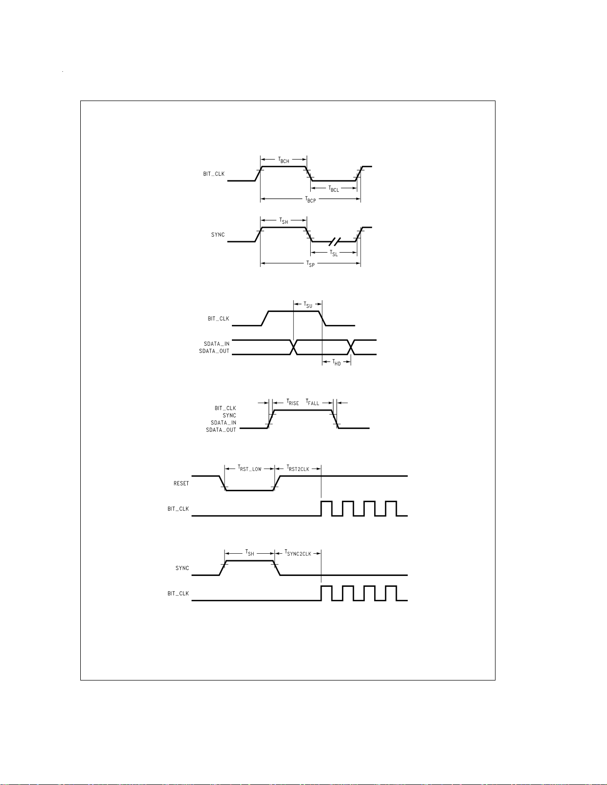
Timing Diagrams
Clocks
DS101035-10
Data Setup and Hold
DS101035-11
Digital Rise and Fall
Cold Reset
Warm Reset
DS101035-12
DS101035-13
DS101035-14
www.national.com5
Page 6
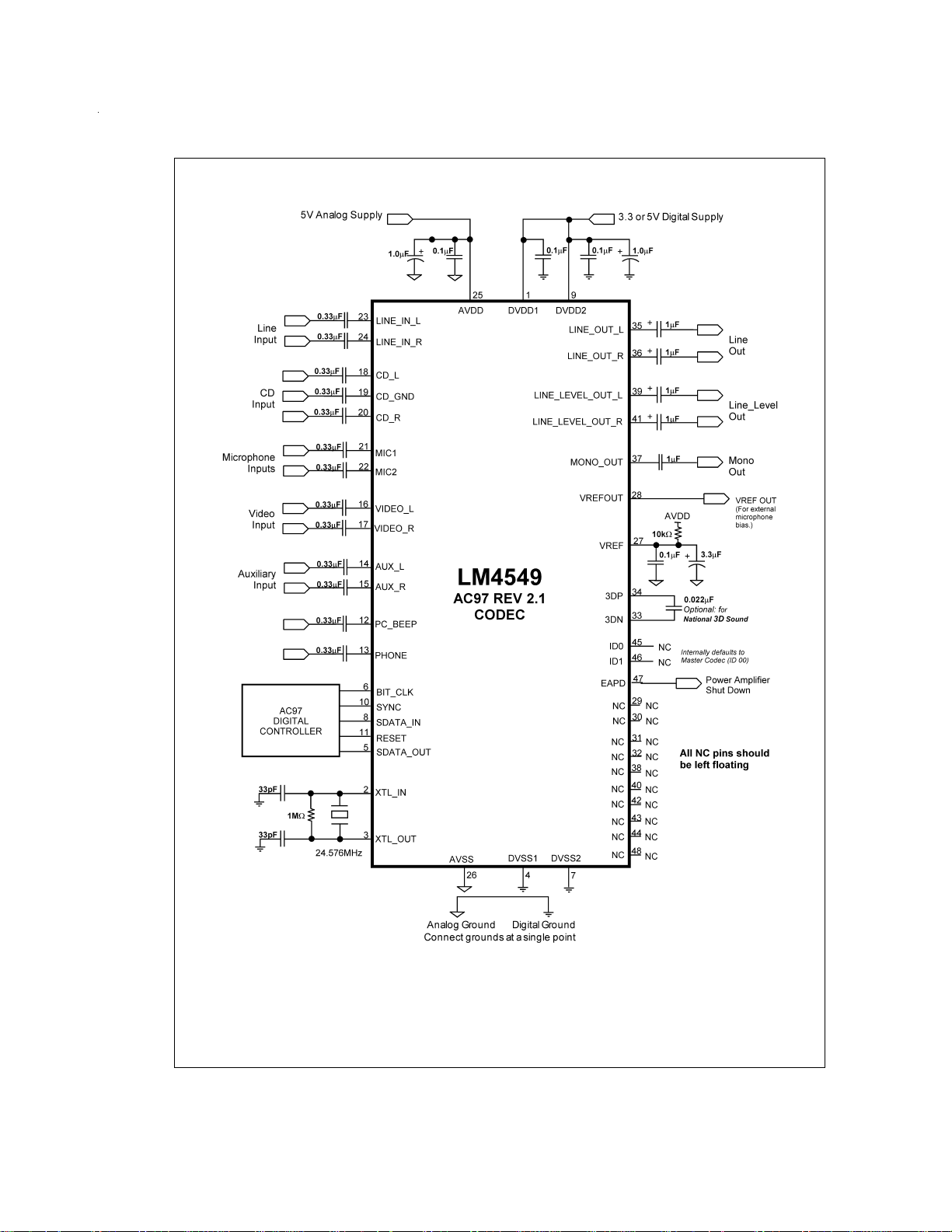
Typical Application
FIGURE 2. LM4549 Typical Application Circuit for a Single Codec Application
www.national.com 6
DS101035-3
Page 7

Connection Diagram
Pin Description
Analog I/O
Name Pin I / O
PC_BEEP 12 I
PHONE 13 I
AUX_L 14 I
DS101035-2
Top View
Order Number LM4549VH
See NS Package Number VBH48A
Functional Description
This is a mono input which gets summed into both the stereo line out and the true line level
out after the National 3D Sound block. The PC_BEEP level can be adjusted from 0dB to
−45dB in 3dB steps, or muted, via register 0Ah. This input is directly connected to the line
output while the reset pin is held active low to allow power on self test tones to be heard
through the audio system.
This is a mono input which gets summed into both the stereo line out and the true line level
out after the National 3D Sound block. The PHONE level can be adjusted from +12dB to
−34.5dB in 1.5dB steps as well as muted via register 0Ch.
This line level input can be routed through the Input Mux and recorded by the left ADC. In
addition, this analog input gets summed into the left output stream. The amount of AUX_L
signal mixed in the left output stream can be adjusted from +12dB to −34.5dB in 1.5dB steps
as well as muted via register 16h.
www.national.com7
Page 8

Pin Description (Continued)
Analog I/O (Continued)
Name Pin I / O
AUX_R 15 I
VIDEO_L 16 I
VIDEO_R 17 I
CD_L 18 I
CD_GND 19 I
CD_R 20 I
MIC1 21 I
MIC2 22 I
LINE_IN_L 23 I
LINE_IN_R 24 I
Functional Description
This line level input can be routed through the Input Mux and recorded by the right ADC. In
addition, this analog input gets summed into the right output stream. The amount of AUX_R
signal mixed in the right output stream can be adjusted from +12dB to −34.5dB in 1.5dB
steps as well as muted via register 16h.
This line level input can be routed through the Input Mux and recorded by the left ADC. In
addition, this analog input gets summed into the left output stream. The amount of VIDEO_L
signal mixed in the left output stream can be adjusted from +12dB to −34.5dB in 1.5dB steps
as well as muted via register 14h.
This line level input can be routed through the Input Mux and recorded by the right ADC. In
addition, this analog input gets summed into the right output stream. The amount of
VIDEO_R signal mixed in the right output stream can be adjusted from +12dB to −34.5dB in
1.5dB steps as well as muted via register 14h.
This line level input can be routed through the Input Mux and recorded by the left ADC. In
addition, this analog input gets summed into the left output stream. The amount of CD_L
signal mixed in the left output stream can be adjusted from +12dB to −34.5dB in 1.5dB steps
as well as muted via register 12h.
This input can be used to reject common mode signals on the CD_L and CD_R inputs.
CD_GND is an AC ground point and not a DC ground point. This input must be AC-coupled
to the source signal’s ground.
This line level input can be routed through the Input Mux and recorded by the right ADC. In
addition, this analog input gets summed into the right output stream. The amount of CD_R
signal mixed in the right output stream can be adjusted from +12dB to −34.5dB in 1.5dB
steps as well as muted via register 12h.
Either MIC1 or MIC2 can be selected via software and routed through the Input Mux for
recording. The 20dB boost circuit is enabled/disabled via register 0Eh. Also, the amount of
mic signal mixed in the output stream can be adjusted from +12dB to −34.5dB in 1.5dB
steps as well as muted via register 0Eh.
This line level input can be routed through the Input Mux and recorded by the left ADC. In
addition, this analog input gets summed into the left output stream. The amount of
LINE_IN_L signal mixed in the left output stream can be adjusted from +12dB to −34.5dB in
1.5dB steps as well as muted via register 10h.
This line level input can be routed through the Input Mux and recorded by the right ADC. In
addition, this analog input gets summed into the right output stream. The amount of
LINE_IN_R signal mixed in the right output stream can be adjusted from +12dB to −34.5dB
in 1.5dB steps as well as muted via register 10h.
LINE_OUT_L 35 O
LINE_OUT_R 36 O
MONO_OUT 37 O
LNLVL_OUT_L 39 O
LNLVL_OUT_R 41 O
www.national.com 8
This is a post-mixed output for the left audio channel. The level of this output can be
adjusted from 0dB to −45dB in 1.5dB steps as well as muted via register 02h.
This is a post-mixed output for the right audio channel. The level of this output can be
adjusted from 0dB to −45dB in 1.5dB steps as well as muted via register 02h.
This line level output is either the post-mixed output or the mic input. The level of this output
can be adjusted from 0dB to −45dB in 1.5dB steps as well as muted via register 06h.
This is a post-mixed output for the left audio channel. The level of this output can be
adjusted from 0dB to −45dB in 1.5dB steps as well as muted via register 04h.
This is a post-mixed output for the right audio channel. The level of this output can be
adjusted from 0dB to −45dB in 1.5dB steps as well as muted via register 04h.
Page 9

Pin Description (Continued)
Digital I/O and Clocking
Name Pin I / O Functional Description
XTL_IN 2 I
XTL_OUT 3 O
SDATA_OUT 5 I
BIT_CLK 6 I/O
SDATA_IN 8 O
SYNC 10 I
RESET# 11 I
ID0 45 I
ID1 46 I
EAPD 47 O
24.576 MHz crystal input. Use a fundamental-mode type crystal. When operating from a
crystal, a 1MΩ resistor must be connected across pins 2 and 3.
24.576 MHz crystal output. When operating from a crystal, a 1MΩ resistor must be
connected across pins 2 and 3.
This data stream contains both control data and DAC audio data. This input is sampled by
the LM4549 on the falling edge of BIT_CLK.
OUTPUT when in Primary Codec Mode: This pin outputs a 12.288 MHz clock which is
derived (internally divided by two) from the 24.576MHz crystal input (XTL_IN).
INPUT when in Secondary Codec Mode (Multiple Codec configurations only): 12.288MHz
clock is to be supplied from an external source, such as from the BIT_CLK of a Primary
Codec.
This data stream contains both control data and ADC audio data. This output is clocked out
by the LM4549 on the rising edge of BIT_CLK.
48kHz sync pulse which signifies the beginning of both the SDATA_IN and SDATA_OUT
serial streams. SYNC must be synchronous to BIT_CLK.
This active low signal causes a hardware reset which returns the control registers to their
default conditions.
ID0 and ID1 set the codec address for multiple codec use where ID0 is the LSB. Connect
these pins to DVdd or GND as required. If these pins are not connected (NC), they default
to Primary codec setting (same as connecting both pins to DVdd). These pins are of inverted
polarity relative to their internal ID0, ID1 registers. If pin 45 is connected to GND, then ID0
will be set to ″1″ internally. Connection to DVdd corresponds to a ″0″ internally.
ID0 and ID1 set the codec address for multiple codec use where ID1 is the MSB. Connect
these pins to DVdd or GND as required. If these pins are not connected (NC), they default
to Primary codec setting (same as connecting both pins to DVdd). These pins are of inverted
polarity relative to their internal ID0, ID1 registers. If pin46 is connected to GND, then ID1
will be set to ″1″ internally. Connection to DVdd corresponds to a ″0″ internally.
The contents of ″Powerdown Ctrl/Stat″ register 26h bit 15 determines the logic level output
on this pin. This pin is to be connected to an external power amplifier’s shutdown pin. If
EAPD=0, then a logic low is output and the external amplifer is enabled. If EAPD=1, the
amplifer is shutdown. Power up default is EAPD=0.
Power Supplies and References
Name Pin I / O Functional Description
AVDD 25 I Analog supply.
AVSS 26 I Analog ground.
DVDD 1,9 I Digital supply.
DVSS 4,7 I Digital ground.
VREF 27 O
VREFOUT 28 O
AFILT1 29 O
AFILT2 30 O
3DP, 3DN 33,34 O
Nominal 2.2V reference output. Not intended to sink or source current. Bypassing of this pin
should be done with short traces to maximize performance.
Nominal 2.2V reference output. Can source up to 5mA of current and can be used to bias a
microphone.
This pin is not used and should be left open (NC). However, a capacitor to ground on this
pin is permitted - it will not affect performance.
This pin is not used and should be left open (NC). However, a capacitor to ground on this
pin is permitted - it will not affect performance.
These pins are used to complete the National 3D Sound circuit. Connect a 0.022µF
capacitor between pins 3DP and 3DN. The National 3D Sound can be turned on and off via
bit D13 in control register 20h. This is a fixed-depth type stereo enhance circuit, thus writing
to register 22h has no effect. If National 3D Sound is not needed, then these pins should be
left as no connect (NC).
www.national.com9
Page 10

Typical Performance Characteristics
ADC Noise Floor
ADC Frequency
Response
DS101035-15
DS101035-19
DAC Noise Floor
DAC Frequency
Response
DS101035-16
DS101035-20
Analog Loopthru
Noise Floor
DS101035-18
True Line Level Out
Noise Floor (Analog Loopthrough)
DS101035-18
www.national.com 10
Page 11

0101h
LM4549 Register Map
00h Reset X 0001101010100000d50h
REG Name D15 D14 D13 D12 D11 D10 D9 D8 D7 D6 D5 D4 D3 D2 D1 D0 Default
True Line Level Out
02h Master Volume Mute X X ML4 ML3 ML2 ML1 ML0 X X X MR4 MR3 MR2 MR1 MR0 8008h
Mute X X ML4 ML3 ML2 ML1 ML0 X X X MR4 MR3 MR2 MR1 MR0 8000h
Volume
04h
Mute XXXXXXXXXXMM4MM3MM2MM1MM08000h
Mono
Master Volume
06h
08h Reserved XXXXXXXXXXXXXXXX0000h
0Ah PC_BEEP Volume Mute XXXXXXXXXXPV3PV2PV1PV0X0000h
0Eh Mic Volume Mute XXXXXXXX20dB X GN4 GN3 GN2 GN1 GN0 8008h
0Ch Phone Volume Mute XXXXXXXXXXGN4GN3GN2GN1GN08008h
10h Line In Volume Mute X X GL4 GL3 GL2 GL1 GL0 X X X GR4 GR3 GR2 GR1 GR0 8808h
12h CD Volume Mute X X GL4 GL3 GL2 GL1 GL0 X X X GR4 GR3 GR2 GR1 GR0 8808h
14h Video Volume Mute X X GL4 GL3 GL2 GL1 GL0 X X X GR4 GR3 GR2 GR1 GR0 8808h
16h Aux Volume Mute X X GL4 GL3 GL2 GL1 GL0 X X X GR4 GR3 GR2 GR1 GR0 8808h
18h PCM Out Vol Mute X X GL4 GL3 GL2 GL1 GL0 X X X GR4 GR3 GR2 GR1 GR0 8808h
1Ah Record Select XXXXXSL2SL1SL0XXXXXSR2SR1SR00000h
1Eh Reserved XXXXXXXXXXXXXXXX0000h
1Ch Record Gain Mute X X X GL3 GL2 GL1 GL0 XXXXGR3GR2GR1GR08000h
0000000100000001
fixed center and
3D Control (3D has
22h
20h General Purpose POP X 3D X X X MIX MS LPBK XXXXXXX0000h
depth)
24h Reserved XXXXXXXXXXXXXXXX0000h
EAPD PR6 PR5 PR4 PR3 PR2 PR1 PR0 XXXXREFANLDACADCna
Powerdown
26h
Ctrl/Stat
28h Extended Audio ID ID1 ID0 XXXXX000XX0X01X001h
XXXXXXXXXXXXXXXVRAXXX0h
SR15 SR14 SR13 SR12 SR11 SR10 SR9 SR8 SR7 SR6 SR5 SR4 SR3 SR2 SR1 SR0 BB80h
Status/Control
Extended Audio
PCM Front DAC
2Ah
2Ch
Rate
32h PCM ADC Rate SR15 SR14 SR13 SR12 SR11 SR10 SR9 SR8 SR7 SR6 SR5 SR4 SR3 SR2 SR1 SR0 BB80h
5Ah Vendor Reserved ---------------- -
www.national.com11
7Ah Vendor Reserved ---------------- -
7Ch Vendor ID1 01001110010100114E53h
7Eh Vendor ID2 01000011001100014331h
Page 12

Application Information
AC Link Serial Interface Protocol
DS101035-4
FIGURE 3. AC 97 Bidirectional Audio Frame
DS101035-6
FIGURE 4. AC Link Audio Output Frame
AC Link Output Frame: SDATA_OUT (output from
controller, input to LM4549)
The audio output frame (output from AC ’97 Controller) contains control and PCM data targeted for the LM4549 control
registers and stereo DAC. The Tag slot, slot 0, contains 16
bits that tell the AC Link interface circuitry on the LM4549 the
validity of the following data slots.
A new audio output frame is signaled with a low to high transition of SYNC. SYNC is synchronous to the rising edge of
BIT_CLK. On the next rising edge of BIT_CLK, the AC ’97
Controller drives SDATA_OUT with the first bit of slot 0. The
LM4549 samples SDATA_OUT on the falling edge of BIT_CLK. The AC ’97 Controller will continue outputting the
SDATA_OUT stream on each successive rising edge of BIT_CLK.
SDATA_OUT Slot 0: Tag Phase
The first bit of slot 0 is designated the ″Valid Frame″ bit. If
this bit is 1, it indicates that the current data frame contains
at least one slot of valid data and the LM4549 will further
sample the next four bits to determine which frames do in
fact have valid data. Valid slots are signified bya1intheir respective slot bit position.
www.national.com 12
FIGURE 5. Start of Audio Output Frame
Bit Description Comment
15 Valid Frame
Control
14
register
address
13
12
Control
register data
Left Playback
PCM Data
1 = This frame has valid
data.
1 = Control Address is
valid.
1 = Control Data is valid.
1 = Left PCM Data is
valid.
DS101035-5
Page 13

Application Information (Continued)
Bit Description Comment
11
Playback
PCM Data
SDATA_OUT Slot 1: Control Address
Slot 1 is used both to write to the LM4549 registers as well
as read back a register’s current value. The MSB of Slot 1
(bit 19) signifies whether the current control operation is a
read or a write. Bits 18 through 12 are used to specify the
register address of the read or write operation. The least significant twelve bits are reserved and should be stuffed with
zeros by the AC’97 controller.
Bits Description Comment
19 Read/Write 0 = Read, 1 = Write
Right
18:12
Control
Register
11:0 Reserved Set to ″0″
SDATA_OUT Slot 2: Control Data
Slot 2 is used to transmit 16 bit control data to the LM4549 in
the event that the current operation is a write operation. The
least significant four bits should be stuffed with zeros by the
AC ’97 controller. If the current operation is a register read,
the entire slot, bits 19 through 0 should be stuffedwith zeros.
1 = Right PCM Data is
valid.
Identifies the Control
Register
Bits Description Comment
19:4
Control
Register Write
Data
Set bits to ″0″ if read
operation
3:0 Reserved Set to ″0″
SDATA_OUT Slot 3: PCM Playback Left Channel
Slot 3 is a 20 bit field used to transmit data intended for the
left DAC on the LM4549. Any unused bits should be padded
with zeros. The LM4549 DAC’s have 18 bit resolution and
thus will use the first 18 bits of the 20 bit PCM stream.
Bits Description Comment
PCM Audio
19:0
Data for Left
Set unused bits to ″0″
DAC
SDATA_OUT Slot 4: PCM Playback Right Channel
Slot 4 is a 20 bit field used to transmit data intended for the
right DAC on the LM4549. Any unused bits should be padded with zeros. The LM4549 DAC’s have 18 bit resolution
and thus will use the first 18 bits of the 20 bit PCM stream.
Bits Description Comment
PCM Audio
19:0
Data for Right
Set unused bits to ″0″
DAC
SDATA_OUT Slots 5-12: Reserved
Set these SDATA_OUT slots to ″0″ as they are not currently
implemented and are reserved for future use.
FIGURE 6. AC Link Audio Input Frame
AC Link Input Frame: SDATA_IN (input to controller,
output from LM4549)
The audio input frame (input to the AC ’97 Digital Controller)
contains status and PCM data from the LM4549 control registers and stereo ADC. The Tag slot, slot 0, contains 16 bits
that tell the AC ’97 Digital Controller whether the LM4549 is
ready and the validity of data from certain device subsections.
A new audio input frame is signaled with a low to high transition of SYNC. SYNC is synchronous to the rising edge of
BIT_CLK. On the next rising edge of BIT_CLK, the LM4549
drives SDATA_IN with the first bit of slot 0. The Digital Controller samples SDATA_IN on the falling edge of BIT_CLK.
The LM4549 will continue outputting the SDATA_IN stream
on each successive rising edge of BIT_CLK. The LM4549
outputs data MSB first, in a MSB justified format. All reserved
bits and slots are stuffed with ″0″ ’s by the LM4549.
DS101035-8
SDATA_IN Slot 0: Codec Status Bits
The first bit of SDATA_IN Slot 0 (bit 15) indicates when the
Codec is ready. The digital controller must probe further to
see which other subsections are ready.
www.national.com13
Page 14

Application Information (Continued)
DS101035-7
FIGURE 7. Start of Audio Input Frame
Bit Description Comment
Codec Ready
15
14
13
12
11
Bit
Slot 1 data
valid
Slot 2 data
valid
Slot 3 data
valid
Slot 4 data
valid
SDATA_IN Slot 1: Status Address / Slot Request Bits
This slot echoes the control register which a read was requested on. The address echoed was initiated by a read request in the previous SDATA_OUT frame, slot 1. Bits 11 and
10 are slot request bits that support Sample Rate Conversion (SRC) functionality. If bit 11is set to 0, then the controller should respond with a valid PCM left sample in slot 3 of
the next frame. If bit 10 is set to 0, then the controller should
respond with a valid PCM right sample in slot 4 of the next
frame. If bits 11 or 10 are set to 1, the controller should not
send data in the next frame. Bits 9 through 2 are unused.
Bits 1 and 0 are reserved and should be set to 0.
Bits Description Comment
19 Reserved Stuffed with ″0″
18:12
Control
Register Index
Slot 3
11
Request bit
(PCM left)
Slot 4
10
Request bit
(PCM right)
0=Not Ready, 1=Ready
Status Address is valid
Status Data is valid
Left Audio PCM Data is
valid
Right Audio PCM Data is
valid
Echo of Control Register
for which data is being
returned.
0 = Controller should
send valid slot 3 data in
the next frame, 1 =
Controller should not
send slot 3 data in the
next frame
0 = Controller should
send valid slot 4 data in
the next frame, 1 =
Controller should not
send slot 4 data in the
next frame
Bits Description Comment
9:2
Other Slot
Request bits
Unused - stuff with ″0″
1,0 Reserved Stuff with ″0″
SDATA_IN Slot 2: Status Data
The slot returns the control register data. The data returned
was initiated by a read request in the previous SDATA_OUT
frame, slot 1.
Bits Description Comment
Control
19:4
Register Read
Data
3:0 Reserved Stuffed with ″0″ ’s
SDATA_IN Slot 3: PCM Record Left Channel
This slot contains the left ADC sample data. The signal to be
digitized is selected via register 1Ah and subsequently
routed through the Input Mux for recording by the left ADC.
This is a 20-bit slot, where the digitized 18-bit PCM data is
output from the codec MSB first and the last remaining 2 bits
will zeros.
Bits Description Comment
19:2
PCM Record
Left Channel
data
18 bit audio sample from
left ADC
1:0 Reserved Stuffed with ″0″’s
SDATA_IN Slot 4: PCM Record Right Channel
This slot contains the right ADC sample data. The signal digitized is selected via register 1Ah and subsequently routed
through the Input Mux for recording by the right ADC. This is
a 20-bit slot, where the digitized 18-bit PCM data is output
from the codec MSB first and the last remaining 2 bits will zeros.
Bits Description Comment
19:2
PCM Record
Right Channel
data
18 bit audio sample from
right ADC
1:0 Reserved Stuffed with ″0″’s
SDATA_IN Slots 5-12: Reserved
These SDATA_INslots are set to ″0″ as they are reserved for
future use.
AC Link Low Power Mode
DS101035-9
FIGURE 8. AC Link Powerdown Timing
www.national.com 14
Page 15

Application Information (Continued)
Register Descriptions
Reset Register (00h)
Writing any value to this register causes a register reset
which changes all of the registers back to their default values. If a read is performed on this register, the LM4549 will
return a value of 0D50h indicating that National 3D Sound is
implemented, 18bit data is supported for both the ADC’s and
DAC’s, and the volume control for True Line Level Out is
supported.
Master Volume Registers (02h, 04h, 06h)
These registers allow the output levels from LINE_OUT, LNLVL_OUT and MONO_OUT to be attenuated or muted.
There are 6-bits of volume control, plus one mute bit. It is a
5-bit volume range, where each step is nominally 1.5dB and
each output can be individually muted by either setting the
most significant bit (Mx5), and/or the mute bit (D15) to ″1.″
Mute Mx5:Mx0 Function
0 00 0000 0dB attenuation
0 01 1111 46.5dB attenuation
0 1X XXXX 46.5dB attenuation
1 XX XXXX mute
Default: 8000h
PC Beep Register (0Ah)
This register controls the level of the PC_BEEP input. The
PC_BEEP can be both attenuated and muted via register
0Ah. Step size is nominally 3dB. The signal present after the
attenuation and mute block is summed into both the left and
right channels.
Mute PV3:0 Function
0 0000 0dB attenuation
0 1111 45dB attenuation
1 XXXX mute
Default: 0000h
Mixer Input Volume Registers (Index 0Ch - 18h)
These registers set the input volume levels including mute.
Each volume control is 5 bit which provides from a range of
+12dB gain to 34.5dB attenuation in 1.5dB steps. For stereo
ports, the left and right levels can be independently set. Muting a given port is accomplished by setting the MSB to 1.
Setting the MSB to 1 for stereo ports mutes both the left and
right channel. Register 0Eh has an additional 20dB boost for
a microphone level input. This is enabled by setting bit 6 of
register 0Eh to 1.
Mute Gx4:Gx0 Function
0 00000 +12dB gain
0 01000 0dB gain
0 11111 34.5dB attenuation
1 XXXXX mute
Default: 8008h (mono regs.), 8808h (stereo regs.)
Record Select Register (1Ah)
This register independently controls the source for the right
and left channel which will be recorded by the stereo ADC.
The default value is 0000h which corresponds to Mic in.
SL2:SL0 Left Record Source
0 Mic
1 CDIn(L)
2 Video In (L)
3 Aux In (L)
4 Line In (L)
5 Stereo Mix (L)
6 Mono Mix (L)
7 Phone
SR2:SR0 Right Record Source
0 Mic
1 CDIn(R)
2 Video In (R)
3 Aux In (R)
4 Line In (R)
5 Stereo Mix (R)
6 Mono Mix (R)
7 Phone
Record (Input) Gain Register (1Ch)
This registers controls the Record (Input) Gain level for the
stereo input selected via the Record Select Control Register
(1Ah). The gain can be programmed from 0dB to +22.5dB in
1.5dB steps. The level for the left and right channel can be
individually controlled. The input can also be muted by setting the MSB to 1.
Mute Gx3:Gx0 Function
0 1111 22.5dB gain
0 0000 0dB gain
1 XXXX mute
Default: 8000h
General Purpose Register (20h)
This register controls many miscellaneous functions implemented on the LM4549. The miscellaneous functions include
POP which allows the PCM to bypass the National 3D
Sound circuitry, 3D which enables or disables the National
3D Sound circuitry, MIX which selects the MONO_OUT
source, MS which selects the microphone mux source and
LPBK which connects the output of the stereo ADC to input
of the stereo DAC. LPBK provides for a digital loopthru path
when enabled.
BIT Function
POP
3D National 3D Sound on / off1=on
MIX Mono output select0=Mix,1=Mic
MS Mic select 0 = Mic1 1 = Mic2
LPBK ADC/DAC loopback
Powerdown Control / Status Register (26h)
This read/write register is used to monitor subsystem readiness and also to program the LM4549 powerdown states.
The lower half of this register is read only with a ″1″, indicating the subsection is ready. Writing to the lower 8 bits will
have no effect.
PCM out path and mute,0=pre3D,1=
post 3D
www.national.com15
Page 16

Application Information (Continued)
When the AC Link ″Codec Ready″ indicator bit (SDATA_IN
slot 0, bit 15) is a ″1″, it indicates that theAC Link andAC ’97
registers are in a fully operational state. The AC ’97 Controller must further probe the Powerdown Control / Status Register to determine exactly which subsections are ready.
BIT Function
REF Vref’s up to nominal level
ANL Analog mixers ready
DAC DAC section ready to accept data
ADC ADC section ready to transmit data
Supported powerdown modes.
BIT Function
PRO PCM in ADC’s and Input Mux powerdown
PR1 PCM out DAC’s powerdown
PR2 Analog Mixer powerdown (VREF still on)
PR3 Analog Mixer powerdown (VREF off)
PR4
PR5 Internal Clk disable
PR6 not used
EAPD External amplifier powerdown
Extended Audio ID Register (28h)
This read only register identifies which AC97 Extended Audio features are supported. The LM4549 provides for VRA
(VariableRate Audio) and Multiple Codec support. VRA is indicated by a ″1″ in the LSB of register 28h. The two MSB’s,
ID1 and ID0, show the current codec configuration as connected via external pins 45 and 46. Note that the external
logic connection to pins 45 and 46 are inverse in polarity to
the internal register setting.
Pin46 (ID1) Pin45 (ID0) Reg 28h ID1 Reg 28h ID0 Codec Mode
NC (not
connected)
DVdd DVdd 0 0 Primary
DVdd GND 0 1 Secondary 1
GND DVdd 1 0 Secondary 2
GND GND 1 1 Secondary 3
Extended Audio Status/Control Register (2Ah)
This read/write register provides status and control of the
VariableSample Rate function. Setting the LSB of this register to ″1″ enables Variable Rate Audio (VRA) mode and allows DAC and ADC sample rates to be programmed via registers 2Ch and 32h.
BIT Function
VRA 0 = VRA off (48kHz fixed), 1 = VRA on
Sample Rate Control Registers (2Ch, 32h)
These read/write registers are used to set the sample rate
for the left and right channels of the DAC (2Ch) and the ADC
(32h). When VariableRate Audio is enabled via bit-0 of Register 2Ah, the sample rates can be programmed, in 1Hz increments, to be any value from 4kHz to 48kHz. Below is a list
of the most common sample rates and their corresponding
register values.
Digital Interface (AC Link) powerdown
(external clk off)
NC (not
connected)
00
Reserved Registers
Do not write to these registers as they are reserved.
SR15:SR0 Sample Rate (Hz)
1F40h 8000
2B11h 11025
3E80h 16000
5622h 22050
AC44h 44100
BB80h 48000
Primary
www.national.com 16
Page 17

17
Page 18

Physical Dimensions inches (millimeters) unless otherwise noted
48-Lead , TQFP,7X7X1.4mm, JEDEC (M)
Order Number LM4549VH
NS Package Number VBH48A
LIFE SUPPORT POLICY
NATIONAL’S PRODUCTS ARE NOT AUTHORIZED FOR USE AS CRITICAL COMPONENTS IN LIFE SUPPORT DEVICES OR SYSTEMS WITHOUT THE EXPRESS WRITTEN APPROVAL OF THE PRESIDENT OF NATIONAL SEMICONDUCTOR CORPORATION. As used herein:
1. Life support devices or systems are devices or systems which, (a) are intended for surgical implant into
the body, or (b) support or sustain life, and whose failure to perform when properly used in accordance
with instructions for use provided in the labeling, can
LM4549 AC ’97 Rev 2.1 Codec with Sample Rate Conversion and National 3D Sound
be reasonably expected to result in a significant injury
2. A critical component is any component of a life support
device or system whose failure to perform can be reasonably expected to cause the failure of the life support
device or system, or to affect its safety or effectiveness.
to the user.
National Semiconductor
Corporation
Americas
Tel: 1-800-272-9959
Fax: 1-800-737-7018
Email: support@nsc.com
www.national.com
National does not assume any responsibility for use of any circuitry described, no circuit patent licenses are implied and National reserves the right at any time without notice to change said circuitry and specifications.
National Semiconductor
Europe
Fax: +49 (0) 1 80-530 85 86
Email: europe.support@nsc.com
Deutsch Tel: +49 (0) 1 80-530 85 85
English Tel: +49 (0) 1 80-532 78 32
Français Tel: +49 (0) 1 80-532 93 58
Italiano Tel: +49 (0) 1 80-534 16 80
National Semiconductor
Asia Pacific Customer
Response Group
Tel: 65-2544466
Fax: 65-2504466
Email: sea.support@nsc.com
National Semiconductor
Japan Ltd.
Tel: 81-3-5639-7560
Fax: 81-3-5639-7507
 Loading...