

Page 1
LM431
Adjustable Precision Zener Shunt Regulator
LM431 Adjustable Precision Zener Shunt Regulator
November 2000
General Description
The LM431 is a 3-terminal adjustable shunt regulator with
guaranteed temperature stability over the entire temperature
range of operation. It is now available in a chip sized package (4-Bump micro SMD) using National’s micro SMD package technology. The output voltage may be set at any level
greater than 2.5V (V
external resistors that act as a voltage divided network. Due
to the sharp turn-on characteristics this device is an excellent replacement for many zener diode applications.
) up to 36V merely by selecting two
REF
Connection Diagrams
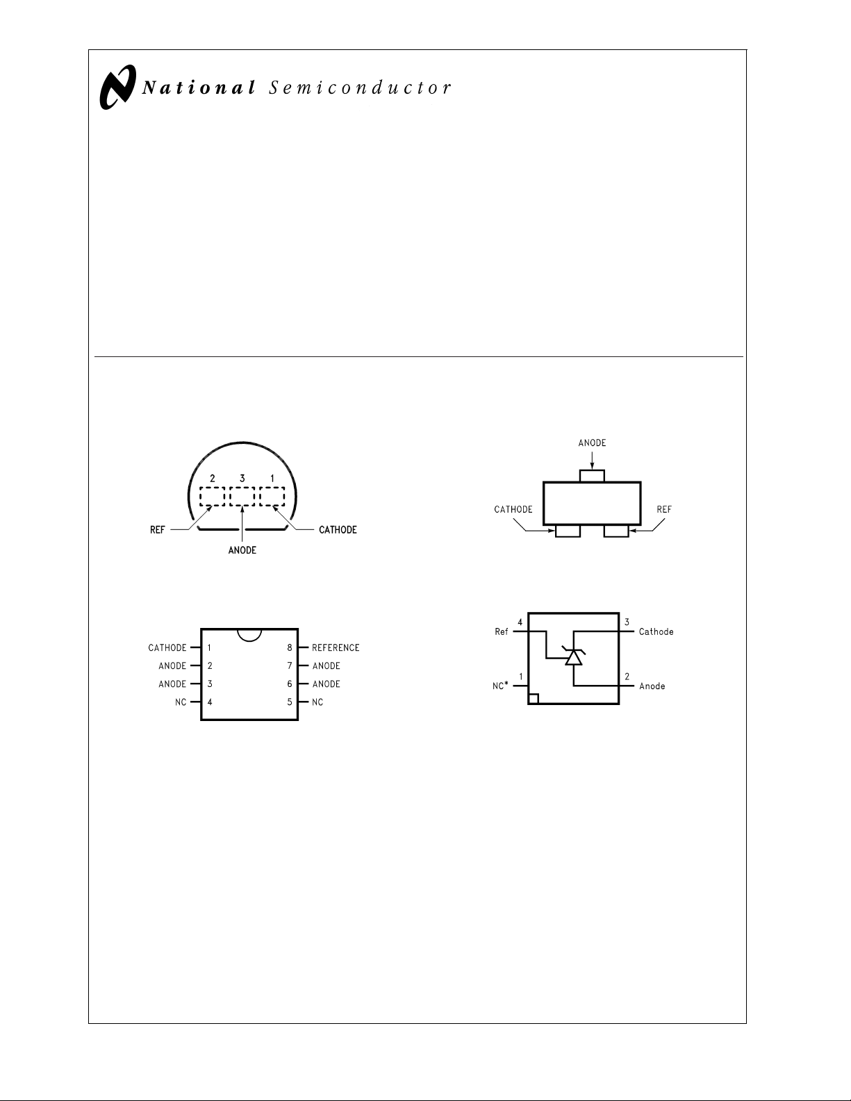
TO-92: Plastic Package
DS010055-1
Top View
SO-8: 8-Pin Surface Mount
Features
n Average temperature coefficient 50 ppm/˚C
n Temperature compensated for operation over the full
temperature range
n Programmable output voltage
n Fast turn-on response
n Low output noise
n LM431 in micro SMD package
n See AN-1112 for micro SMD considerations
SOT-23: 3-Lead Small Outline
DS010055-28
Top View
4-Bump micro SMD
DS010055-54
DS010055-2
Top view
Note:*NC = Not internally connected. Must be electrically isolated from the
rest of the circuit for the microSMD package.
© 2000 National Semiconductor Corporation DS010055 www.national.com
Top View
(bump side down)
Page 2
Ordering Information
LM431
Package Typical Accuracy Order Number/Package Marking Temperature
0.5% 1% 2%
TO-92 LM431CCZ/
LM431CCZ
LM431CIZ/
LM431CIZ
SO-8 LM431CCM/
431CCM
LM431CIM/
431CIM
SOT-23 LM431CCM3/
N1B
LM431CIM3
N1A
micro SMD
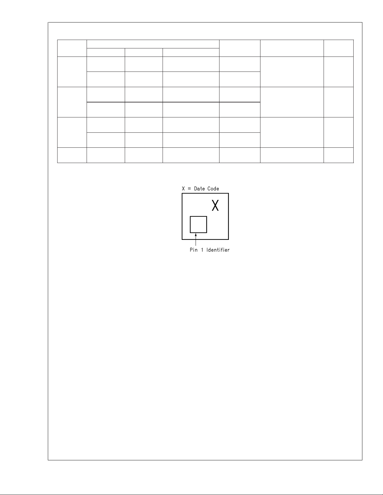
Note 1: The micro SMD package marking is a 1 digit manufacturing Date Code only
––
LM431BCZ/
LM431BCZ
LM431BIZ/
LM431BIZ
LM431BCM/
431BCM
LM431BIM/
431BIM
LM431BCM3/
N1D
LM431BIM3
N1C
LM431ACZ/
LM431ACZ
LM431AIZ/
LM431AIZ
LM431ACM/
LM431ACM
LM431AIM/
LM431AIM
LM431ACM3/
N1F
LM431AIM3
N1E
LM431AIBP
LM431AIBPX(Note 1)
micro SMD Top View Marking Example
Range
0˚C to +70˚C
−40˚C to +85˚C
0˚C to +70˚C
−40˚C to +85˚C
0˚C to +70˚C
−40˚C to +85˚C
−40˚C to +85˚C
Transport Media NSC
Drawing
Rails Z03A
Rails and Tape &Reel M08A
Rails and Tape &Reel MF03A
250 Units Tape and Reel
3k Units Tape and Reel
BPA04AFB
DS010055-56
www.national.com 2
Page 3
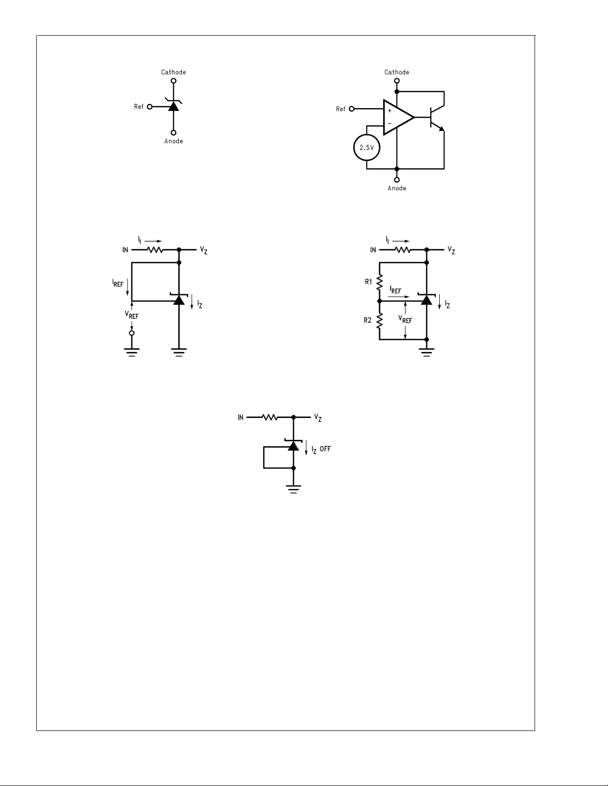
Symbol and Functional Diagrams
DS010055-99
DC Test Circuits
LM431
DS010055-55
DS010055-4
FIGURE 1. Test Circuit for VZ=V
FIGURE 3. Test Circuit for Off-State Current
REF
Note: VZ=V
FIGURE 2. Test Circuit for V
DS010055-6
(1 + R1/R2) + I
REF
REF
•
R1
DS010055-5
>
V
Z
REF
www.national.com3
Page 4
Absolute Maximum Ratings (Note 2)
LM431
If Military/Aerospace specified devices are required,
please contact the National Semiconductor Sales Office/
Distributors for availability and specifications.
Storage Temperature Range −65˚C to +150˚C
Operating Temperature Range
Reference Voltage −0.5V
Reference Input Current 10 mA
Internal Power Dissipation (Notes 3, 4)
TO-92 Package
SO-8 Package
SOT-23 Package
micro SMD Package 0.30W
Industrial (LM431xI) −40˚C to +85˚C
Commercial (LM431xC) 0˚C to +70˚C
Soldering Information
Infrared or Convection (20 sec.) 235˚C
Wave Soldering (10 sec.) 260˚C (lead temp.)
Cathode Voltage 37V
Operating Conditions
Min Max
Cathode Voltage V
Cathode Current 1.0 mA 100 mA
REF
Continuous Cathode Current −10 mA to +150 mA
LM431
Electrical Characteristics
TA= 25˚C unless otherwise specified
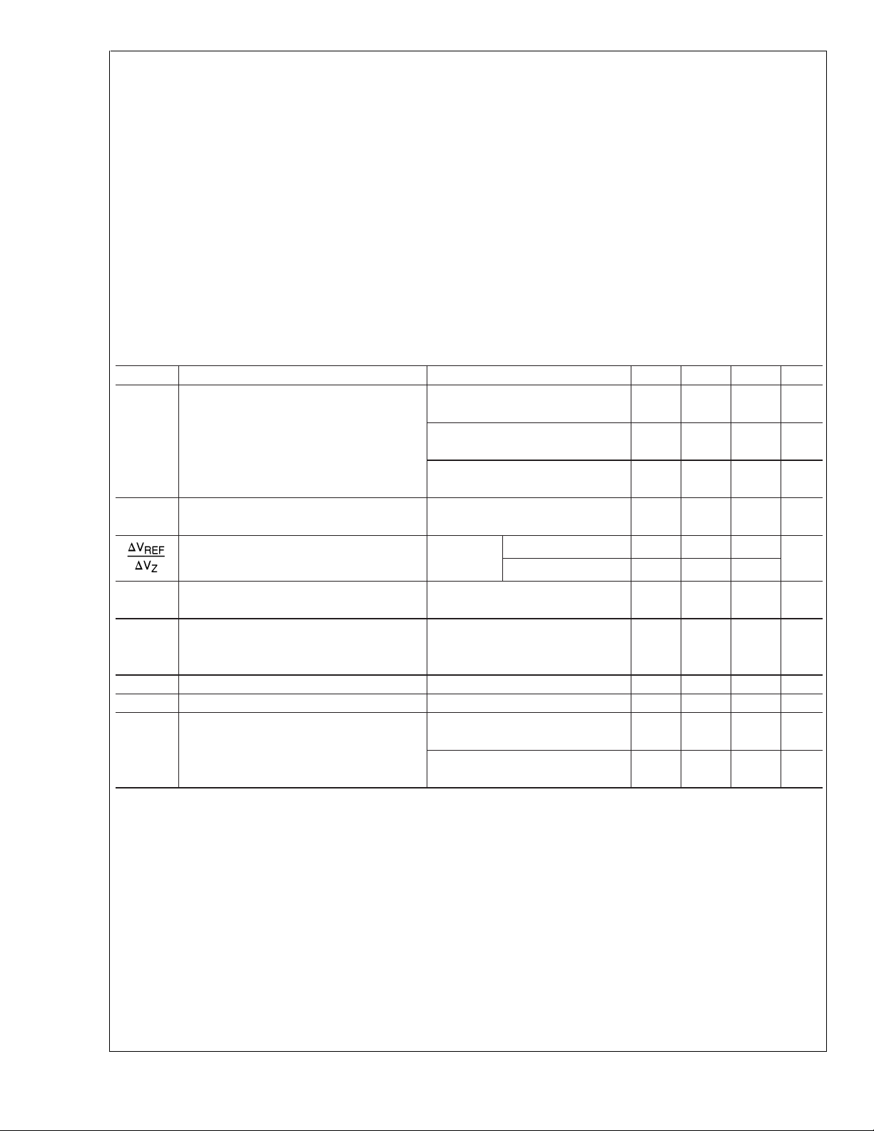
Symbol Parameter Conditions Min Typ Max Units
V
REF
V
DEV
I
REF
∝
I
REF
I
Z(MIN)
I
Z(OFF)
r
Z
Note 2: Absolute Maximum Ratings indicate limits beyond which damage to the device may occur. Electrical specifications do not apply when operating the device
beyond its rated operating conditions.
Note 3: T
Note 4: Ratings apply to ambient temperature at 25˚C. Above this temperature, derate the TO-92 at 6.2 mW/˚C, the SO-8 at 6.5 mW/˚C, the SOT-23 at 2.2 mW/˚C
and the micro SMD at 3mW/˚C.
Note 5: Deviation of reference input voltage, V
Reference Voltage VZ=V
LM431A
VZ=V
LM431B
VZ=V
LM431C
Deviation of Reference Input Voltage Over VZ=V
Temperature (Note 5) T
= Full Range
A
Ratio of the Change in Reference Voltage IZ=10mA VZfrom V
to the Change in Cathode Voltage
(Figure 2 )
= 10 mA 2.440 2.495 2.550 V
REF,II
(Figure 1 )
= 10 mA 2.470 2.495 2.520 V
REF,II
(Figure 1 )
= 10 mA 2.485 2.500 2.510 V
REF,II
(Figure 1 )
= 10 mA, 8.0 17 mV
REF,II
(Figure 1 )
to 10V −1.4 −2.7
REF
VZfrom 10V to 36V −1.0 −2.0
Reference Input Current R1=10kΩ,R2=∞, 2.0 4.0 µA
I
=10mA
I
(Figure 2 )
Deviation of Reference Input Current over R1=10kΩ,R2=∞,
Temperature I
Minimum Cathode Current for Regulation VZ=V
Off-State Current VZ= 36V, V
Dynamic Output Impedance (Note 6) VZ=V
= 150˚C.
J Max
, is defined as the maximum variation of the reference input voltage over the full temperature range.
DEV
= 10 mA, 0.4 1.2 µA
I
T
= Full Range
A
REF
REF
Frequency = 0 Hz
VZ=V
REF
Frequency = 0 Hz
(Figure 2 )
(Figure 1 )
=0V
REF
(Figure 3 )
0.4 1.0 mA
0.3 1.0 µA
, LM431A, 0.75 Ω
(Figure 1 )
, LM431B, LM431C 0.50 Ω
(Figure 1 )
0.78W
0.81W
0.28W
37V
mV/V
www.national.com 4
Page 5
LM431
Electrical Characteristics
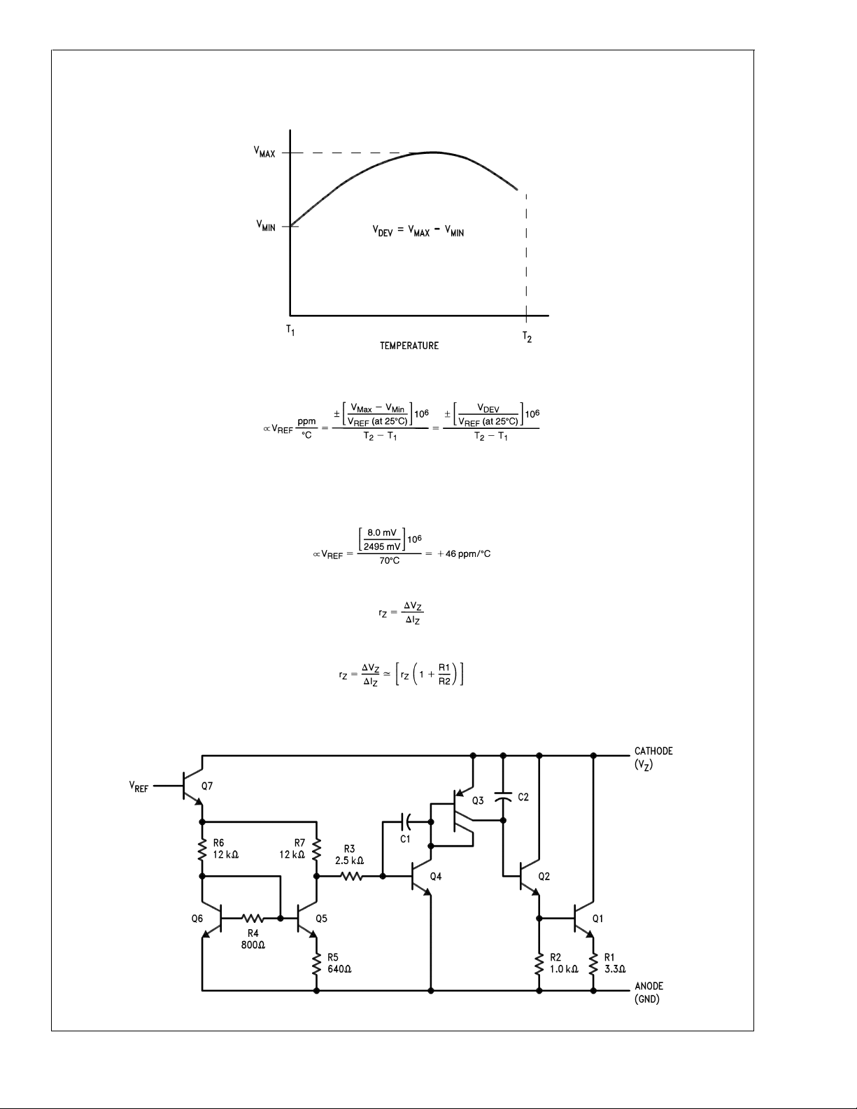
The average temperature coefficient of the reference input voltage,∝V
(Continued)
, is defined as:
REF
LM431
DS010055-7
Where:
T
= full temperature change (0-70˚C).
2−T1
∝
can be positive or negative depending on whether the slope is positive or negative.
V
REF
Example: V
Note 6: The dynamic output impedance, rZ, is defined as:
When the device is programmed with two external resistors, R1 and R2, (see
DEV
= 8.0 mV, V
= 2495 mV, T2−T1= 70˚C, slope is positive.
REF
Equivalent Circuit
Figure 2
), the dynamic output impedance of the overall circuit, rZ, is defined as:
DS010055-3
www.national.com5
Page 6
Typical Performance Characteristics
LM431
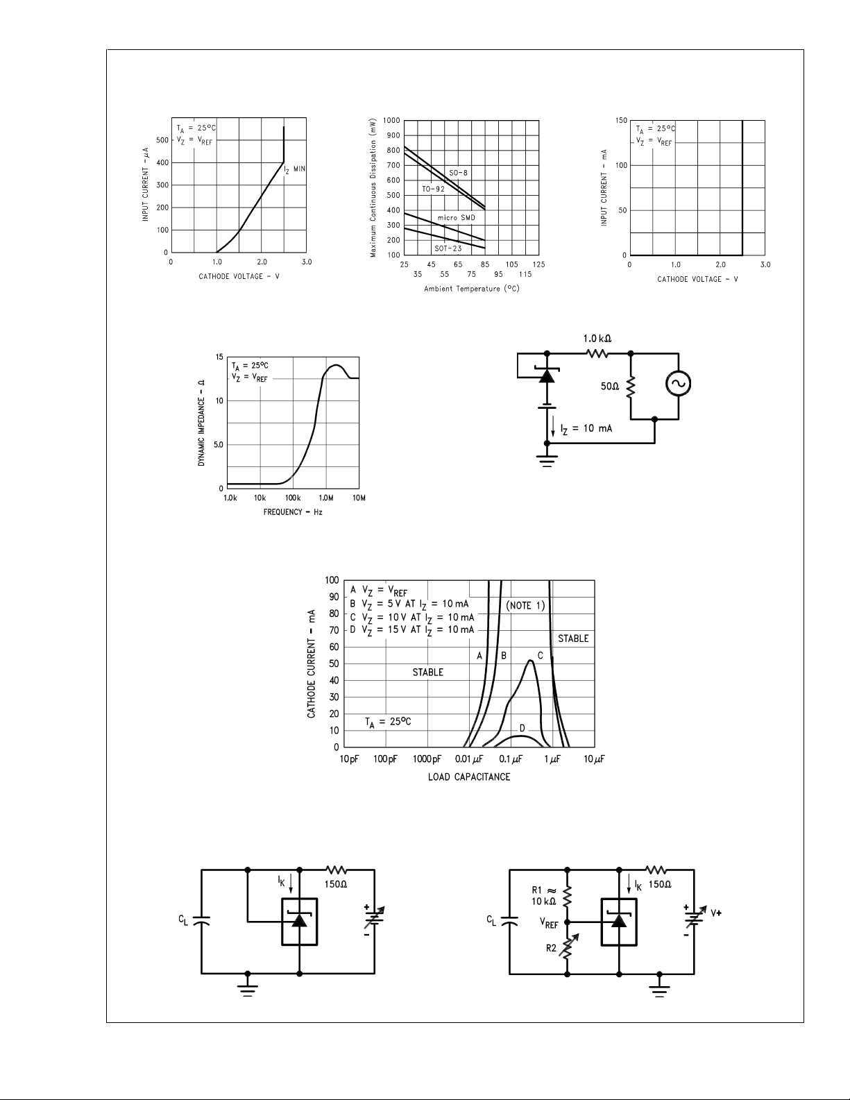
Input Current vs V
Z
Thermal Information
Input Current vs V
Z
DS010055-29
Dynamic Impedance vs Frequency
Stability Boundary Conditions
DS010055-30
DS010055-31
DS010055-10
DS010055-9
DS010055-11
Note: The areas under the curves represent conditions that may cause the device to oscillate. For curves B, C, and D, R2 and V+were adjusted to establish
the initial V
Test Circuit for Curve A Above
and IZconditions with CL=0.V+and CLwere then adjusted to determine the ranges of stability.
Z
Test Circuit for Curves B, C and D Above
DS010055-12
DS010055-13
www.national.com 6
Page 7
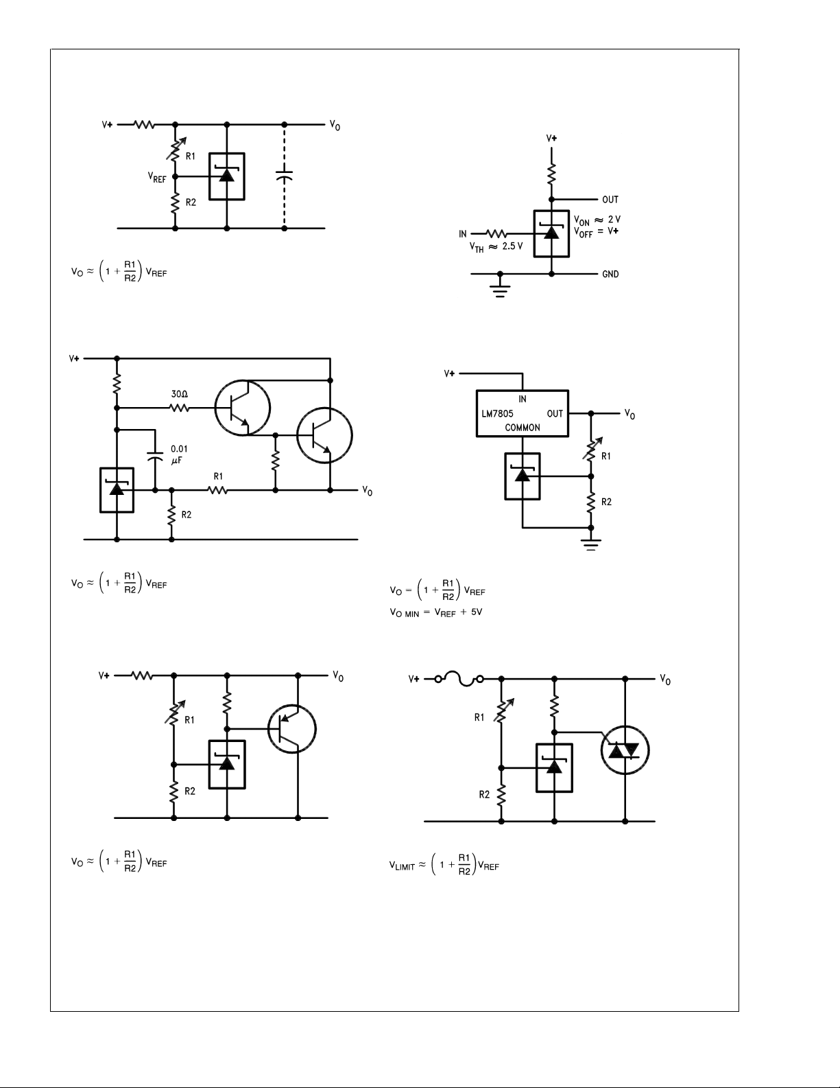
Typical Applications
LM431
Shunt Regulator
Series Regulator
Single Supply Comparator with
Temperature Compensated Threshold
DS010055-14
DS010055-15
Output Control of a Three
Terminal Fixed Regulator
Higher Current Shunt Regulator
DS010055-16
DS010055-18
DS010055-17
Crow Bar
DS010055-19
www.national.com7
Page 8
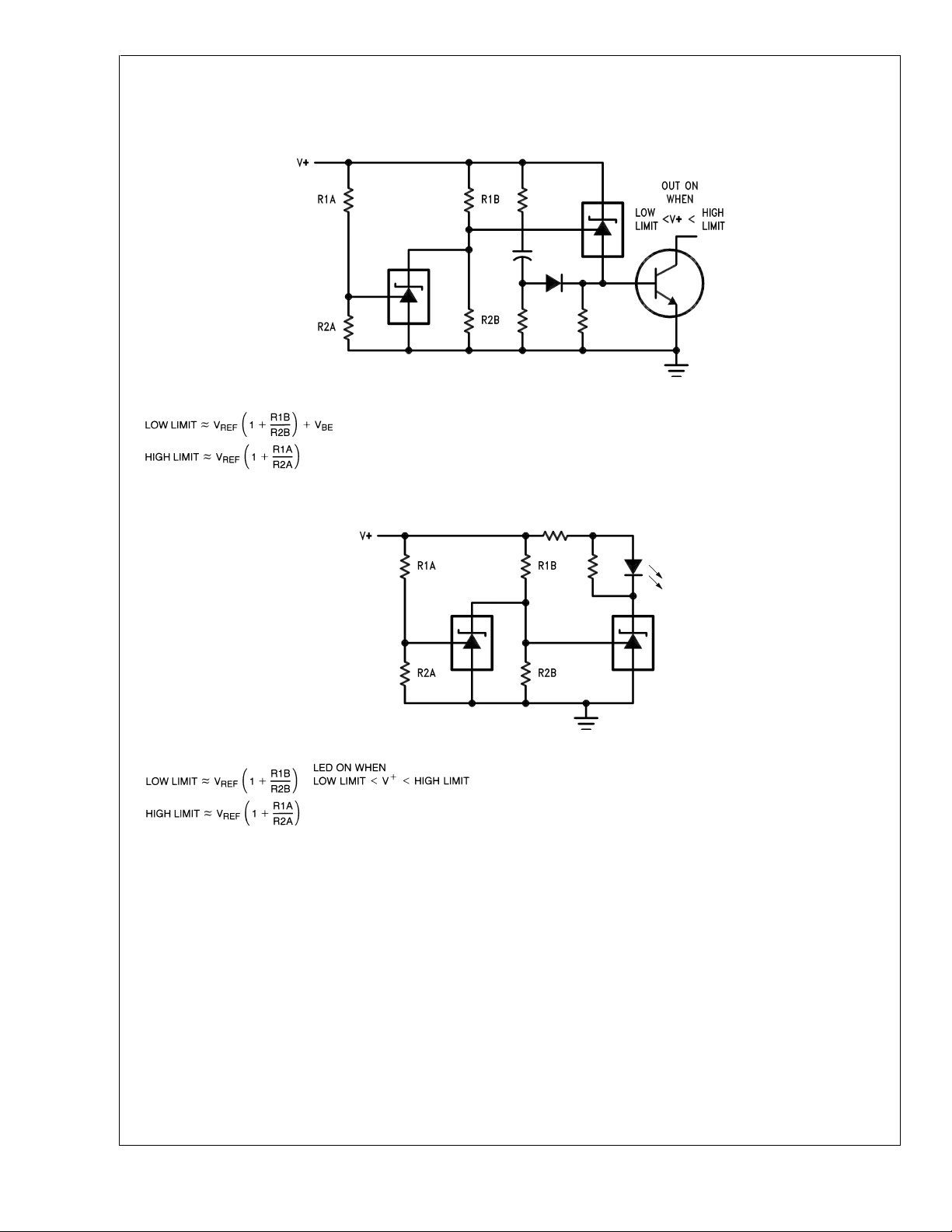
Typical Applications (Continued)
LM431
Over Voltage/Under Voltage
Protection Circuit
DS010055-20
Voltage Monitor
www.national.com 8
DS010055-21
Page 9
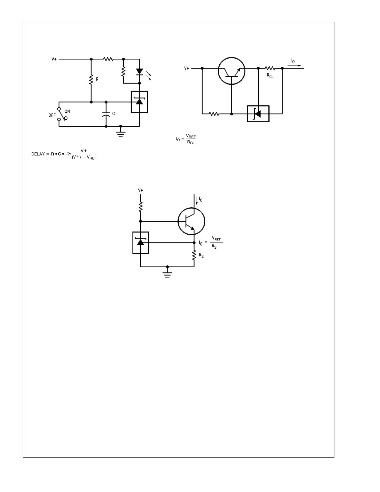
Typical Applications (Continued)
LM431
Delay Timer
Current Limiter or Current Source
DS010055-23
DS010055-22
Constant Current Sink
Application Info
1.0 Mounting
To ensure that the geometry of the micro SMD package
maintains good physical contact with the printed circuit
board, pin 1 (NC) must be soldered to the pcb. Please see
AN-1112 for more detailed information regarding board
mounting techniques for the micro SMD package.
DS010055-24
2.0 LM431 micro SMD Light Sensitivity
When the LM431 micro SMD package is exposed to bright
sunlight, normal office fluorescent light, and other LED’s and
lasers, it operates within the guaranteed limits specified in
the electrical characteristics table.
www.national.com9
Page 10
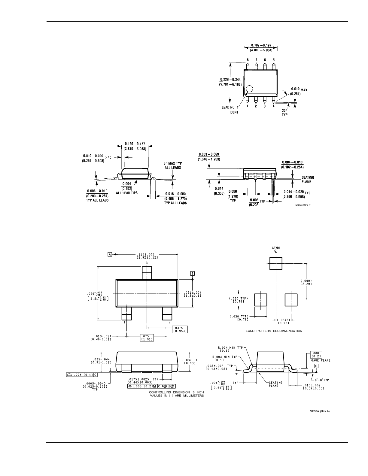
Physical Dimensions inches (millimeters) unless otherwise noted
LM431
NS Package Number M08A
SOT-23 Molded Small Outline Transistor Package (M3)
NS Package Number MF03A
www.national.com 10
Page 11
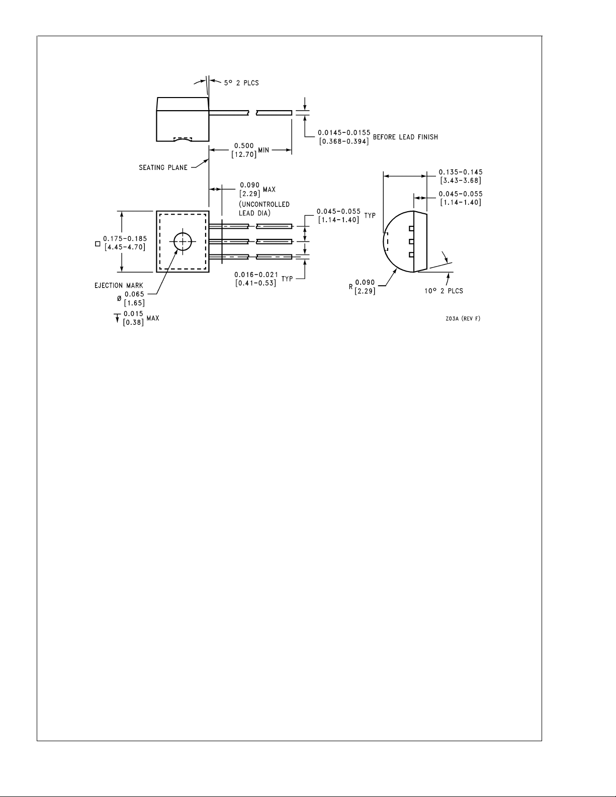
Physical Dimensions inches (millimeters) unless otherwise noted (Continued)
LM431
NS Package Number Z03A
www.national.com11
Page 12
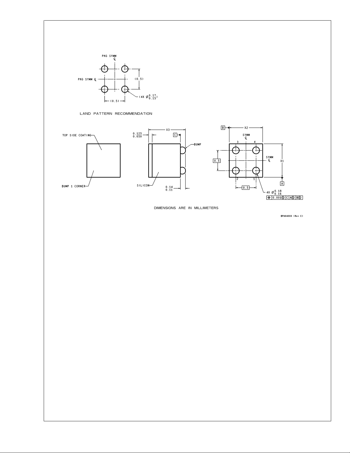
Physical Dimensions inches (millimeters) unless otherwise noted (Continued)
LM431
NOTES: UNLESS OTHERWISE SPECIFIED
1. EPOXY COATING
2. 63Sn/37Pb EUTECTIC BUMP
3. RECOMMEND NON-SOLDER MASK DEFINED LANDING PAD.
4. PIN 1 IS ESTABLISHED BY LOWER LEFT CORNER WITH RESPECT TO TEXT ORIENTATION. REMAINING PINS ARE
NUMBERED.
5. XXX IN DRAWING NUMBER REPRESENTS PACKAGE SIZE VARIATION WHERE X1 IS PACKAGE WIDTH, X2 IS
PACKAGE LENGTH AND X3 IS PACKAGE HEIGHT.
6. REFERENCE JEDEC REGISTRATION MO-211, VARIATION BA.
4-Bump micro SMD
X1 = 0.777 X2 = 0.904 X3 = 0.850
NS Package Number BPA04AFB
www.national.com 12
Page 13

Notes
LM431 Adjustable Precision Zener Shunt Regulator
LIFE SUPPORT POLICY
NATIONAL’S PRODUCTS ARE NOT AUTHORIZED FOR USE AS CRITICAL COMPONENTS IN LIFE SUPPORT
DEVICES OR SYSTEMS WITHOUT THE EXPRESS WRITTEN APPROVAL OF THE PRESIDENT AND GENERAL
COUNSEL OF NATIONAL SEMICONDUCTOR CORPORATION. As used herein:
1. Life support devices or systems are devices or
systems which, (a) are intended for surgical implant
into the body, or (b) support or sustain life, and
whose failure to perform when properly used in
accordance with instructions for use provided in the
2. A critical component is any component of a life
support device or system whose failure to perform
can be reasonably expected to cause the failure of
the life support device or system, or to affect its
safety or effectiveness.
labeling, can be reasonably expected to result in a
significant injury to the user.
National Semiconductor
Corporation
Americas
Tel: 1-800-272-9959
Fax: 1-800-737-7018
Email: [email protected]
www.national.com
National does not assume any responsibility for use of any circuitry described, no circuit patent licenses are implied and National reserves the right at any time without notice to change said circuitry and specifications.
National Semiconductor
Europe
Fax: +49 (0) 180-530 85 86
Email: [email protected]
Deutsch Tel: +49 (0) 69 9508 6208
English Tel: +44 (0) 870 24 0 2171
Français Tel: +33 (0) 1 41 91 8790
National Semiconductor
Asia Pacific Customer
Response Group
Tel: 65-2544466
Fax: 65-2504466
Email: [email protected]
National Semiconductor
Japan Ltd.
Tel: 81-3-5639-7560
Fax: 81-3-5639-7507
 Loading...