

Page 1
LM431A/LM431B/LM431C
Programmable Shunt Regulator
www.fairchildsemi.com
Features
• Programmable Output Voltage to 36 Volts
• Low Dynamic Output Impedance 0.20 Typical
• Sink Curren t Capability of 1.0 to 100mA
• Equivalent Full-Range Temperature Coefficient of
50ppm/°C Typical
• Temperature Compensated for Operation Over Full Rated
Operating Temperature Range
• Low Output Noise Voltage
• Fast Turn-on Response
Description
The LM431A/LM431B/LM431C are three terminal output
adjustable regulators with thermal stability over operating
temperature range. The output voltage can be set any value
between V
two external resistors. These devices have a typical dynamic
output imped ance of 0.2Ω Act ive output circ uit provides a
sharp turn-on characteristic, making these devices excellent
replacement for Zener Diodes in many applications.
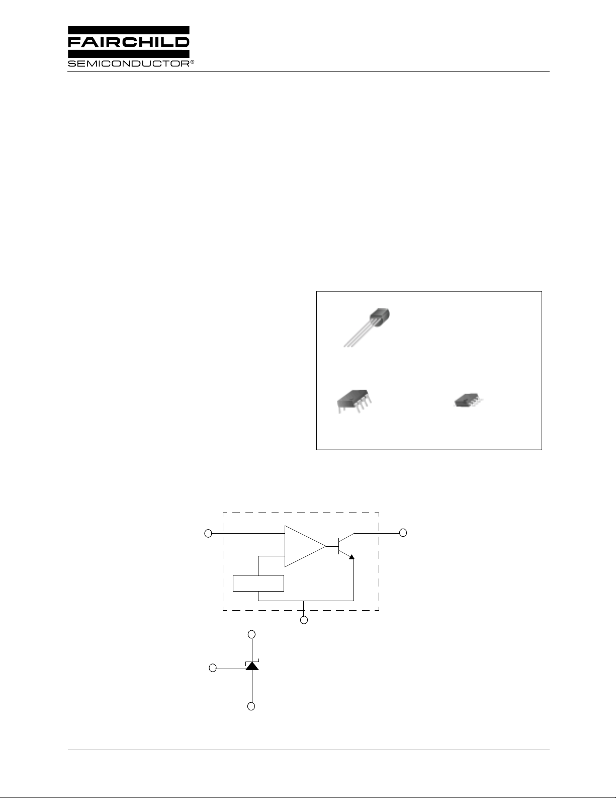
TO-92
1
1. Ref 2. Anode 3. Cathode
8-DIP 8-SOP
1.Cathode 2.3 .4.5.7.NC
6.Anode 8.Ref
(approximately 2.5 volts) and 36 volts with
REF
1
1.Cathode 2.3.6.7.A no de
4.5.NC 8.Ref
1
Internal Block Diagram
REFERENCE
REFERENCE (R)
©2002 Fairchild Semiconductor Corporation
CATHODE
2.5 Vref
ANODE
CA THODE (K)
ANODE (A)
Rev. 1.0.6
Page 2
LM431A/LM431B/LM431C
Absolute Maximum Ratings
(Operating temperature range applies unless otherwise specified.)
Parameter Symbol Value Unit
Cathode Voltage V
Cathode Current Range (Continuous) I
Reference Input Current Range I
KA
KA
REF
37 V
-100 ~ +150 mA
0.05 ~ +10 mA
Power Dissipation
M, Z Suffix Package
N Suffix Package
P
D
770
mW
1000
Operating Temperature Range
LM431xC
LM431xI -40 ~ +85 °C
Junction Temperature T
Storage Temperature Range T
T
OPR
J
STG
-25 ~ +85 °C
150 °C
-65 ~ +150 °C
Recommended Operating Conditions
Parameter Symbol Min Typ Max Unit
Cathode Voltage V
Cathode Current I
KA
KA
V
REF
1.0 - 100 mA
-36V
2
Page 3
Electrical Characteristics
(TA = +25°C, unless otherwise specified)
LM431A/LM431B/LM431C
Parameter Symbol Conditions
Reference
Input Voltage
Deviation of
Reference
Input Voltage
OverTemperature
Ratio of
Change in
Reference
Input Voltage
to the Change
in Cathode
Voltage
Reference
Input Current
Deviation of
Reference
Input Current
Over Full
Temperature
Range
Minimum
Cathode Current for
Regulation
Off - Stage
Cathode
Current
Dynamic
Impedance Z
V
REF
V
∆
∆
V
∆
V
∆
I
REF
I
∆
REF
I
KA(MIN)VKA=VREF
I
KA(OFF)
REF
T
REF
KA
/
/
/∆T
V
= V
KA
V
KA=VREF
T
MIN≤TA≤TMAX
IKA
=10mA
IKA=10mA,
=10kΩ,R2=∞
R
1
I
=10mA,
KA
=10kΩ,R2=∞
R
1
T
=Full Range
A
VKA=36V,
V
=0
REF
VKA=V
KA
KA
=1 to 100mA
I
f ≥1.0kHz
, I
REF
, IKA=10mA
∆
V
∆
10V
,
REF
KA
VKA=10V-
REF
VKA=36V-
LM431A LM431B LM431C
Min. Typ. Max. Min. Typ. Max. Min. Typ. Max.
Unit
=10mA 2.450 2.500 2.550 2.470 2.495 2.520 2.482 2.495 2.508 V
-
4.5 17
-
4.5 17
-
4.5 17 mV
- -1.0 -2.7 - -1.0 -2.7 - -1.0 -2.7
mV/V
- -0.5 -2.0 - -0.5 -2.0 - -0.5 -2.0
-1.54 -1.54 -1.54
-
0.4 1.2
-
0.4 1.2
-
0.4 1.2
µ
µ
- 0.45 1.0 - 0.45 1.0 - 0.45 1.0 mA
- 0.05 1.0 - 0.05 1.0 - 0.05 1.0
µ
- 0.15 0.5 - 0.15 0.5 - 0.15 0.5 Ω
A
A
A
Note1
•LM431
•LM431
C : T
X
I : T
X
MIN
MIN
= -25 °C, T
= -40°C, T
MAX
MAX
= +85°C
= +85°C
3
Page 4
LM431A/LM431B/LM431C
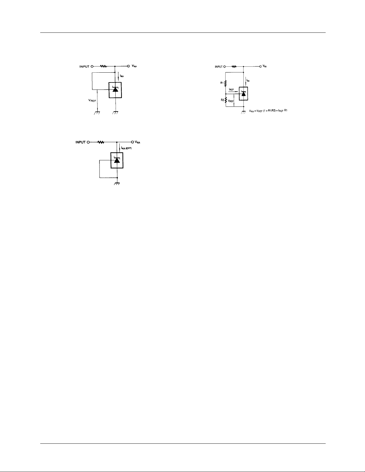
Test Circuits
LM431A/B/C
LM431A/B/C
Figure 1. Test Circuit for VKA=V
LM431A/B/C
Figure 3. Test Circuit for l
KA(OFF)
REF
Figure 2. Test Circuit for V
KA
≥≥≥≥V
REF
4
Page 5

Typical Performance Characteristic s
LM431A/LM431B/LM431C
Figure 6.
Figure 4.
Cathode Current vs. Cathode Voltage
Change In Reference Input Voltage vs.
Cathode Voltage
Figure 5.
Cathode Current vs. Cathode Voltage
Figure7. Dynamic Impedance Frequency
Figure 8. Small Signal Voltage Amplification vs. Frequency
Figure 9.
Pulse Response
5
Page 6

LM431A/LM431B/LM431C
Typical Performance Characte ristic s
140
A VKA = Vref
120
100
80
60
40
, CATHODE CURRENT(mA)
K
I
20
0
100p 1n 10n 100n 1µ 10µ
= 5.0 V @ IK = 10
B V
KA
C VKA = 10 V @ IK = 10
D VKA = 15 V @ IK = 10
TA = 25oC
CL, LOAD CAPACITANCE
Figure 10. Stability Boundary Conditions
A
mA
mA
mA
B
C
D
(Continued)
6
Page 7

Typical Application
LM431A/LM431B/LM431C
R
1
V
1
------ -+
=
O
Figure 11. Shunt Regulator
V
ref
R
2
LM431A/B/C
Figure 12
LM431A/B/C
Figure 14. Current Limit or Current Source
VOV
=
LM7805/MC7805
LM431A/B/C
.
Output Control for
-
minal Fixed RegulatorThree- Ter-
R
1
1
------ -+
ref
R
2
R
V
1
------ -+
=
O
R
Figure 13. High Current Shunt Regulator
LM431A/B/C
Figure 15. Constant-Current Sink
1
V
ref
2
LM431A/B/C
7
Page 8

LM431A/LM431B/LM431C
Mechanical Dimensions
Package
Dimensions in millimeters
0.46
±0.10
4.58
+0.25
–0.15
TO-92
±0.20
4.58
±0.40
14.47
1.27TYP
[1.27
±0.20
1.27TYP
]
3.60
±0.20
[1.27
±0.20
]
0.38
+0.10
–0.05
3.86MAX
(0.25)
+0.10
±0.10
1.02
–0.05
0.38
(R2.29)
8
Page 9

LM431A/LM431B/LM431C
Mechanical Dimensions
Package
#1
#4
(Continued)
8-SOP
1.55
±0.20
0.061
#8
MAX
5.13
#5
±0.008
0.202
Dimensions in millimeters
0.1~0.25
MIN
0.004~0.001
0.56
0.022
()
±0.008
±0.20
4.92
0.194
±0.10
±0.004
0.006
-0.002
0.50
0.020
+
0.004
±0.20
±0.008
0.15
-0.05
+
0.10
6.00
0.236
3.95
0.156
5.72
0.225
±0.30
±0.012
±0.20
±0.008
0.071
0~8°
1.80
MAX
MAX0.10
MAX0.004
1.27
0.050
0.41
0.016
9
Page 10

LM431A/LM431B/LM431C
Mechanical Dimensions
Package
6.40
±0.20
±0.008
0.252
#1
#4 #5
#8
(Continued)
MAX
9.60
0.378
8-DIP
±0.008
±0.20
9.20
0.362
Dimensions in millimeters
0.79
0.031
()
±0.10
0.46
2.54
±0.004
0.018
0.100
±0.10
±0.004
1.524
0.060
0~15°
7.62
0.300
0.25
0.010
5.08
0.200
3.40
0.134
+0.10
–0.05
+0.004
–0.002
MAX
±0.20
±0.008
0.33
0.013
MIN
3.30
0.130
±0.30
±0.012
10
Page 11

Ordering Information
Product Number Output Voltage Tolerance Package Operating Temperature
LM431CCZ
LM431CCM 8-SOP
LM431BCZ
LM431BCM 8-SOP
0.5%
1%
LM431ACN
LM431ACZ TO-92
2%
LM431ACM 8-SOP
LM431CIZ
LM431CIM 8-SOP
LM431BIZ
LM431BIM 8-SOP
LM431AIZ
LM431AIM 8-SOP
0.5%
1%
2%
TO-92
TO-92
8-DIP
TO-92
TO-92
TO-92
-25 ~ +85
-40 ~ +85
LM431A/LM431B/LM431C
°
C
°
C
11
Page 12

LM431A/LM431B/LM431C
DISCLAIMER
FAIRCHILD SEMICONDUCTOR RESERVES THE RIGHT TO MAKE CHANGES WITHOUT FURT HER NOTICE TO ANY
PRODUCTS HEREI N TO IMPROVE RELIABILITY, FUNCTIO N OR DESIGN. FAIRCH IL D DOES NOT ASSUME ANY
LIABILITY ARISING OUT OF THE APPLICATION OR USE OF ANY PRODUCT OR CIRCUIT DESCRIBED HEREIN; NEITHER
DOES IT CONVEY ANY LICENSE UNDER IT S PATENT RIGHTS, NOR THE RIGHTS OF OTHE RS.
LIFE SUPPORT POL I CY
FAIRCHILD’S PR ODUCTS ARE NOT AUTH ORIZED FOR USE AS C RITICAL COMPONENT S IN LIFE SUPPORT DE VICES
OR SYSTEMS WITHOUT THE EXPRESS WRITTEN APPROVAL OF THE PRESIDENT OF FAIRCHILD SEMICONDUCTOR
CORPORATION. As used herein :
1. Life support devices or systems are devices or systems
which, (a) are intended for surgical implant into the body,
or (b) support or sustain life, and (c) whose failure to
perform when properly used in accordance with
2. A critical component in any component of a life support
device or sy stem whose fai lure to perform can be
reasonably expec ted to cause the failur e of the life support
device or system, or to affect its safety or effec t iv ene ss .
instructions for use provided in the labeling, can be
reasonably expected to result in a significant injury of the
user.
www.fairchildsemi.com
8/20/02 0.0m 001
2002 Fairchild Semiconductor Corporation
Stock#DSxxxxxxxx
 Loading...