

Datasheet LM4041DIM3-ADJ, LM4041CIM3-ADJ, LM4041CIM3-1.2, LM4040CIM3-5.0, LM4040CIM3-2.5 Datasheet (MICREL)
...Page 1
LM4040/4041 Micrel
LM4040/4041
Precision Micropower Shunt Voltage Reference
General Description
Ideal for space critical applications, the LM4040 and LM4041
precision voltage references are available in the subminiature (3mm × 1.3mm) SOT-23 surface-mount package.
The LM4040 is the available in fixed reverse breakdown
voltages of 2.500V, 4.096V and 5.000V. The LM4041 is
available with a fixed 1.225V or an adjustable reverse breakdown voltage.
The LM4040 and LM4041’s advanced design eliminates the
need for an external stabilizing capacitor while ensuring
stability with any capacitive load, making them easy to use.
The minimum operating current ranges from 60µA for the
LM4041-1.2 to 74µA for the LM4040-5.0. LM4040 versions
have a maximum operating current of 15mA. LM4041
versions have a maximum operating current of 12mA.
The LM4040 and LM4041 utilizes zener-zap reverse breakdown voltage trim during wafer sort to ensure that the prime
parts have an accuracy of better than ±0.1% (A grade) at
25°C. Bandgap reference temperature drift curvature correction and low dynamic impedance ensure stable reverse
breakdown voltage accuracy over a wide range of operating
temperatures and currents.
Features
• Small SOT-23 package
• No output capacitor required
• Tolerates capacitive loads
• Fixed reverse breakdown voltages of 1.225, 2.500V,
4.096V and 5.000V
• Adjustable reverse breakdown version
• Contact Micrel for parts with extended temperature
range.
Key Specifications
• Output voltage tolerance (A grade, 25°C) .. ±0.1% (max)
• Low output noise (10Hz to 100Hz)
LM4040 ................................................35µV
LM4041 ................................................20µV
RMS
RMS
(typ)
(typ)
• Wide operating current range
LM4040 ................................................ 60µA to 15mA
LM4041 ................................................ 60µA to 12mA
• Industrial temperature range ..................–40°C to +85°C
• Low temperature coefficient ................100ppm/°C (max)
Applications
• Battery-Powered Equipment
• Data Acquisition Systems
• Instrumentation
• Process Control
• Energy Management
• Product Testing
• Automotive Electronics
• Precision Audio Components
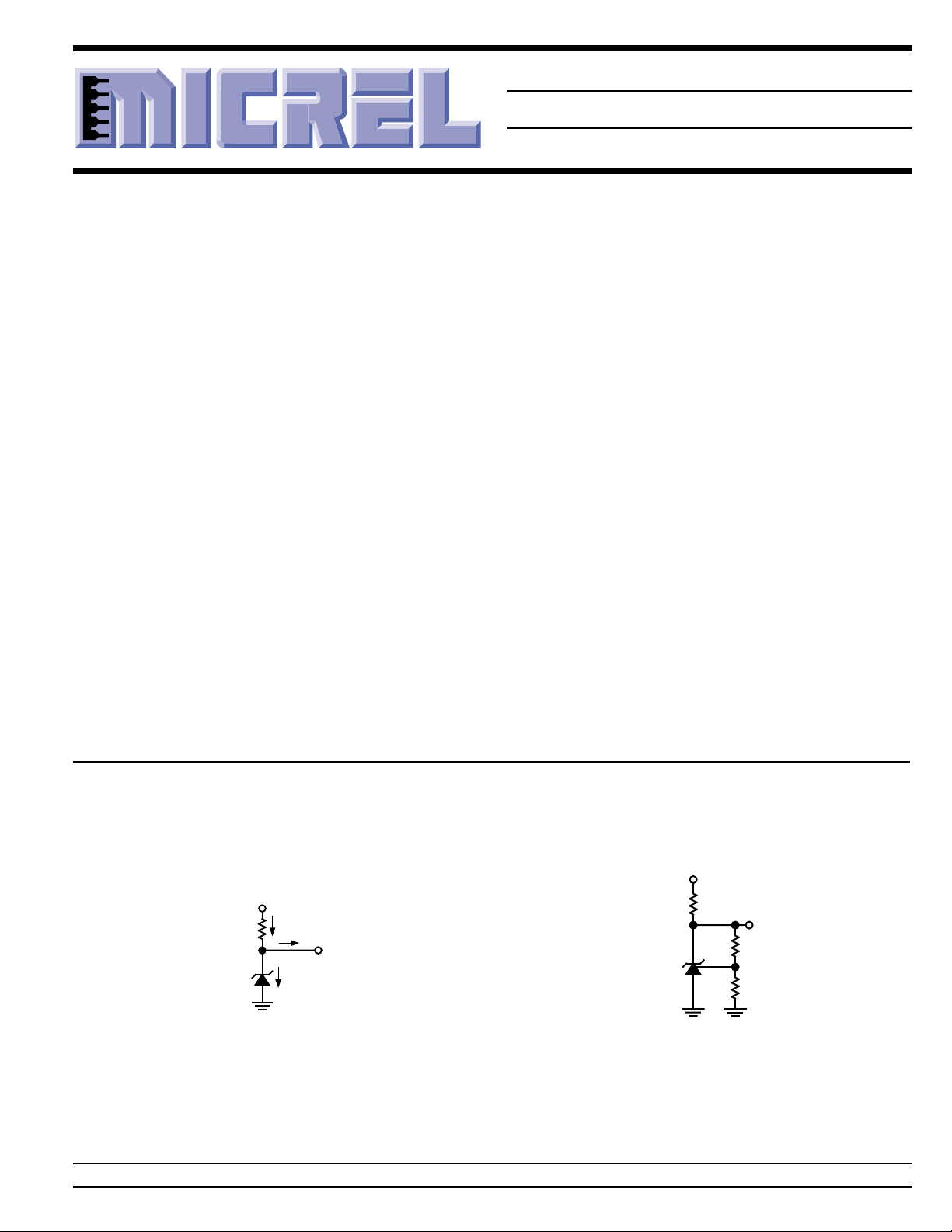
Typical Applications
V
S
V
S
IQ + I
R
S
V
R
LM4040
LM4041
Figure 1. LM4040, LM4041 Fixed
Shunt Regulator Application
Micrel, Inc. • 1849 Fortune Drive • San Jose, CA 95131 • USA • tel + 1 (408) 944-0800 • fax + 1 (408) 944-0970 • http://www.micrel.com
L
I
L
V
O
I
Q
Adjustable
Figure 2. LM4041 Adjustable
Shunt Regulator Application
January 2000 1 LM4040/4041
LM4041
R
S
V
R
V
O
R
1
VO = 1.233 (R2/R1 + 1)
R
2
Page 2
LM4040/4041 Micrel
Pin Configuration
1
+
3
–
2
Pin 3 must float or
be connected to pin 2.
Fixed Version
SOT-23 (M3) Package
Top View
Ordering Information
Part Number * Voltage Accuracy,
Temp. Coefficient
LM4040AIM3-2.5 2.500V ±0.1%, 100ppm/°C
LM4040BIM3-2.5 2.500V ±0.2%, 100ppm/°C
LM4040CIM3-2.5 2.500V ±0.5%, 100ppm/°C
LM4040DIM3-2.5 2.500V ±1.0%, 150ppm/°C
LM4040AIM3-4.1 4.096V ±0.1%, 100ppm/°C
LM4040BIM3-4.1 4.096V ±0.2%, 100ppm/°C
LM4040CIM3-4.1 4.096V ±0.5%, 100ppm/°C
LM4040DIM3-4.1 4.096V ±1.0%, 150ppm/°C
LM4040AIM3-5.0 5.000V ±0.1%, 100ppm/°C
LM4040BIM3-5.0 5.000V ±0.2%, 100ppm/°C
LM4040CIM3-5.0 5.000V ±0.5%, 100ppm/°C
LM4040DIM3-5.0 5.000V ±1.0%, 150ppm/°C
1
FB
3 –
+
2
Adjustable Version
SOT-23 (M3) Package
Top View
Part Number * Voltage Accuracy,
Temp. Coefficient
LM4041AIM3-1.2 1.225V ±0.1%, 100ppm/°C
LM4041BIM3-1.2 1.225V ±0.2%, 100ppm/°C
LM4041CIM3-1.2 1.225V ±0.5%, 100ppm/°C
LM4041DIM3-1.2 1.225V ±1.0%, 150ppm/°C
LM4041CIM3-ADJ 1.24V to 10V ±0.5%, 100ppm/°C
LM4041DIM3-ADJ 1.24V to 10V ±1.0%, 150ppm/°C
SOT-23 Package Markings
Example Field Code
R _ _ 1st Character R = Reference
Example: R2C represents
±
0.5%
(LM4040CIM3-2.5)
Reference, 2.500V,
LM4040/4041 2 January 2000
Example Field Code
_ 2 _ 2nd Character 1 = 1.225V
2 = 2.500V
4 = 4.096V
5 = 5.000V
A = Adjustable
Example Field Code
_ _ A 3rd Character A = ±0.1%
B = ±0.2%
C = ±0.5%
D = ±1.0%
Note: If 3rd character is omitted, container will
indicate tolerance.
Page 3
LM4040/4041 Micrel
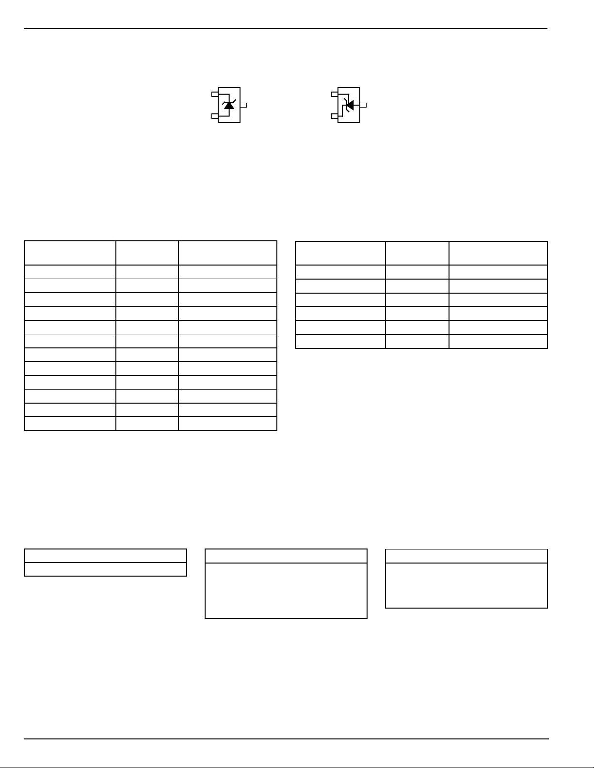
Functional Diagram
LM4040, LM4041 Fixed
Functional Diagram
LM4041 Adjustable
+
V
REF
FB
+
Absolute Maximum Ratings
Reverse Current.........................................................20mA
Forward Current .........................................................10mA
Maximum Output Voltage
LM4041-Adjustable ...................................................15V
Power Dissipation at TA = 25°C (Note 2) ................306mW
Storage Temperature ............................... –65°C to +150°C
Lead Temperature
Vapor phase (60 seconds) .............................. +215°C
Infrared (15 seconds) ...................................... +220°C
ESD Susceptibility
Human Body Model (Note 3).................................2kV
Machine Model (Note 3) ......................................200V
Operating Ratings (Notes 1 and 2)
Temperature Range
(T
≤ TA ≤ T
MIN
Reverse Current
LM4040-2.5 .......................................... 60µA to 15mA
LM4040-4.1 .......................................... 68µA to 15mA
LM4040-5.0 .......................................... 74µA to 15mA
LM4041-1.2 .......................................... 60µA to 12mA
LM4041-ADJ ........................................ 60µA to 12mA
Output Voltage Range
LM4041-ADJ .......................................... 1.24V to 10V
).......................... –40°C ≤ TA ≤ +85°C
MAX
January 2000 3 LM4040/4041
Page 4

LM4040/4041 Micrel
LM4040-2.5 Electrical Characteristics
Boldface limits apply for TA = TJ = T
Breakdown Voltage tolerance of ±0.1%, ±0.2%, ±0.5%, and ±1.0 respectively.
Symbol Parameter Conditions Typical Units
V
R
Reverse Breakdown Voltage IR = 100µA 2.500 V
Reverse Breakdown Voltage I
Tolerance ±19 ±21 ±29 mV (max)
I
RMIN
∆V
R
Minimum Operating Current 45 µA
/∆T Average Reverse Breakdown IR = 10mA 20 ppm/°C
Voltage Temperature I
Coefficient IR = 100µA 15 ppm/°C (max)
/∆IRReverse Breakdown Voltage I
∆V
R
Change with Operating 0.8 0.8 0.8 mV (max)
Current Change 1.0 1.0 1.0 mV (max)
Z
e
∆V
R
N
R
Reverse Dynamic Impedance IR = 1mA, f = 120Hz 0.3 Ω
Wideband Noise IR = 100µA
Reverse Breakdown Voltage t = 1000hrs
Long Term Stability T = 25°C ±0.1°C 120 ppm
MIN
to T
; all other limits TA = TJ = 25°C. The grades A, B, C, and D designate initial Reverse
MAX
LM4040AIM3 LM4040BIM3 LM4040CIM3
(Note 4) Limits Limits Limits (Limit)
(Note 5) (Note 5) (Note 5)
= 100µA ±2.5 ±5.0 ±12 mV (max)
R
60 60 60 µA (max)
65 65 65 µA (max)
= 1mA 15 100 100 100 ppm/°C (max)
R
≤ IR 1mA 0.3 mV
RMIN
1mA ≤ I
15mA 2.5 mV
R
0.6 0.6 0.6 mV (max)
8.0 8.0 8.0 mV (max)
IAC = 0.1 I
R
0.8 0.8 0.9 Ω (max)
10Hz ≤ f ≤ 10kHz 35 µV
IR = 100µA
RMS
Symbol Parameter Conditions Typical Units
LM4040DIM3
(Note 4) Limits (Limit)
(Note 5)
V
R
I
RMIN
Reverse Breakdown Voltage IR = 100µA 2.500 V
Reverse Breakdown Voltage I
Tolerance ±49 mV (max)
= 100µA ±25 mV (max)
R
Minimum Operating Current 45 µA
65 µA (max)
70 µA (max)
/∆T Average Reverse Breakdown IR = 10mA 20 ppm/°C
∆V
R
Voltage Temperature I
Coefficient IR = 100µA 15 ppm/°C (max)
/∆IRReverse Breakdown Voltage I
∆V
R
Change with Operating 1.0 mV (max)
= 1mA 15 150 ppm/°C (max)
R
≤ IR 1mA 0.3 mV
RMIN
Current Change 1.2 mV (max)
1mA ≤ I
15mA 2.5 mV
R
8.0 mV (max)
10.0 mV (max)
Z
e
∆V
R
N
R
Reverse Dynamic Impedance IR = 1mA, f = 120Hz 0.3 Ω
IAC = 0.1 I
R
1.1 Ω (max)
Wideband Noise IR = 100µA
10Hz ≤ f ≤ 10kHz 35 µV
RMS
Reverse Breakdown Voltage t = 1000hrs
Long Term Stability T = 25°C ±0.1°C 120 ppm
IR = 100µA
LM4040/4041 4 January 2000
Page 5

LM4040/4041 Micrel
LM4040-4.1 Electrical Characteristics
Boldface limits apply for TA = TJ = T
Breakdown Voltage tolerance of ±0.1%, ±0.2%, ±0.5%, and ± 1.0% respectively.
Symbol Parameter Conditions Typical Units
V
R
Reverse Breakdown Voltage IR = 100µA 4.096 V
Reverse Breakdown Voltage I
Tolerance ±31 ±35 mV (max)
I
RMIN
∆V
R
Minimum Operating Current 50 µA
/∆T Average Reverse Breakdown IR = 10mA 30 ppm/°C
Voltage Temperature I
Coefficient IR = 100µA 20 ppm/°C (max)
/∆IRReverse Breakdown Voltage I
∆V
R
Change with Operating 0.9 0.9 mV (max)
Current Change 1.2 1.2 mV (max)
Z
e
∆V
R
N
R
Reverse Dynamic Impedance IR = 1mA, f = 120Hz 0.5 Ω
Wideband Noise IR = 100µA
Reverse Breakdown Voltage t = 1000hrs
Long Term Stability T = 25°C ±0.1°C 120 ppm
MIN
to T
; all other limits TA = TJ = 25°C. The grades A, B, C, and D designate initial Reverse
MAX
LM4040AIM3 LM4040BIM3
(Note 4) Limits Limits (Limit)
(Note 5) (Note 5)
= 100µA ±4.1 ±8.2 mV (max)
R
68 68 µA (max)
73 73 µA (max)
= 1mA 20 100 100 ppm/°C (max)
R
≤ IR 1mA 0.5 mV
RMIN
1mA ≤ I
15mA 3.5 mV
R
7.0 7.0 mV (max)
10.0 10.0 mV (max)
IAC = 0.1 I
R
1.0 1.0 Ω (max)
10Hz ≤ f ≤ 10kHz 80 µV
IR = 100µA
RMS
Symbol Parameter Conditions Typical Units
LM4040CIM3 LM4040DIM3
(Note 4) Limits Limits (Limits)
(Note 5) (Note 5)
V
R
I
RMIN
Reverse Breakdown Voltage IR = 100µA 4.096 V
Reverse Breakdown Voltage I
Tolerance ±47 ±81 mV (max)
= 100µA ±20 ±41 mV (max)
R
Minimum Operating Current 50 µA
68 73 µA (max)
73 78 µA (max)
/∆T Average Reverse Breakdown IR = 10mA 30 ppm/°C
∆V
R
Voltage Temperature I
Coefficient IR = 100µA 20 ppm/°C (max)
/∆IRReverse Breakdown Voltage I
∆V
R
Change with Operating 0.9 1.2 mV (max)
= 1mA 20 100 150 ppm/°C (max)
R
≤ IR 1mA 0.5 mV
RMIN
Current Change 1.2 1.5 mV (max)
1mA ≤ I
15mA 3.0 mV
R
7.0 9.0 mV (max)
10.0 13.0 mV (max)
Z
e
∆V
R
N
R
Reverse Dynamic Impedance IR = 1mA, f = 120Hz 0.5 Ω
IAC = 0.1 I
R
1.0 1.3 Ω (max)
Wideband Noise IR = 100µA
10Hz ≤ f ≤ 10kHz 80 µV
RMS
Reverse Breakdown Voltage t = 1000hrs
Long Term Stability T = 25°C ±0.1°C 120 ppm
IR = 100µA
January 2000 5 LM4040/4041
Page 6

LM4040/4041 Micrel
LM4040-5.0 Electrical Characteristics
Boldface limits apply for TA = TJ = T
Breakdown Voltage tolerance of ±0.1%, ±0.2%, ±0.5%, and ± 1.0% respectively.
Symbol Parameter Conditions Typical Units
V
R
Reverse Breakdown Voltage IR = 100µA 5.000 V
Reverse Breakdown Voltage I
Tolerance ±38 ±43 mV (max)
I
RMIN
∆V
R
Minimum Operating Current 54 µA
/∆T Average Reverse Breakdown IR = 10mA 30 ppm/°C
Voltage Temperature I
Coefficient IR = 100µA 20 ppm/°C (max)
/∆IRReverse Breakdown Voltage I
∆V
R
Change with Operating 1.0 1.0 mV (max)
Current Change 1.4 1.4 mV (max)
Z
e
∆V
R
N
R
Reverse Dynamic Impedance IR = 1mA, f = 120Hz 0.5 Ω
Wideband Noise IR = 100µA
Reverse Breakdown Voltage t = 1000hrs
Long Term Stability T = 25°C ±0.1°C 120 ppm
MIN
to T
; all other limits TA = TJ = 25°C. The grades A, B, C, and D designate initial Reverse
MAX
LM4040AIM3 LM4040BIM3
(Note 4) Limits Limits (Limit)
(Note 5) (Note 5)
= 100µA ±5.0 ±10 mV (max)
R
74 74 µA (max)
80 80 µA (max)
= 1mA 20 100 100 ppm/°C (max)
R
≤ IR 1mA 0.5 mV
RMIN
1mA ≤ I
15mA 3.5 mV
R
8.0 8.0 mV (max)
12.0 12.0 mV (max)
IAC = 0.1 I
R
1.1 1.1 Ω (max)
10Hz ≤ f ≤ 10kHz 80 µV
IR = 100µA
RMS
Symbol Parameter Conditions Typical Units
LM4040CIM3 LM4040DIM3
(Note 4) Limits Limits (Limits)
(Note 5) (Note 5)
V
R
I
RMIN
Reverse Breakdown Voltage IR = 100µA 5.000 V
Reverse Breakdown Voltage I
Tolerance ±58 ±99 mV (max)
= 100µA ±25 ±50 mV (max)
R
Minimum Operating Current 54 µA
74 79 µA (max)
80 85 µA (max)
/∆T Average Reverse Breakdown IR = 10mA 30 ppm/°C
∆V
R
Voltage Temperature I
Coefficient IR = 100µA 20 ppm/°C (max)
/∆IRReverse Breakdown Voltage I
∆V
R
Change with Operating 1.0 1.3 mV (max)
= 1mA 20 100 150 ppm/°C (max)
R
≤ IR 1mA 0.5 mV
RMIN
Current Change 1.3 1.8 mV (max)
1mA ≤ I
15mA 3.5 mV
R
8.0 10.0 mV (max)
12.0 15.0 mV (max)
Z
e
∆V
R
N
R
Reverse Dynamic Impedance IR = 1mA, f = 120Hz 0.5 Ω
IAC = 0.1 I
R
1.1 1.5 Ω (max)
Wideband Noise IR = 100µA
10Hz ≤ f ≤ 10kHz 80 µV
RMS
Reverse Breakdown Voltage t = 1000hrs
Long Term Stability T = 25°C ±0.1°C 120 ppm
IR = 100µA
LM4040/4041 6 January 2000
Page 7
LM4040/4041 Micrel
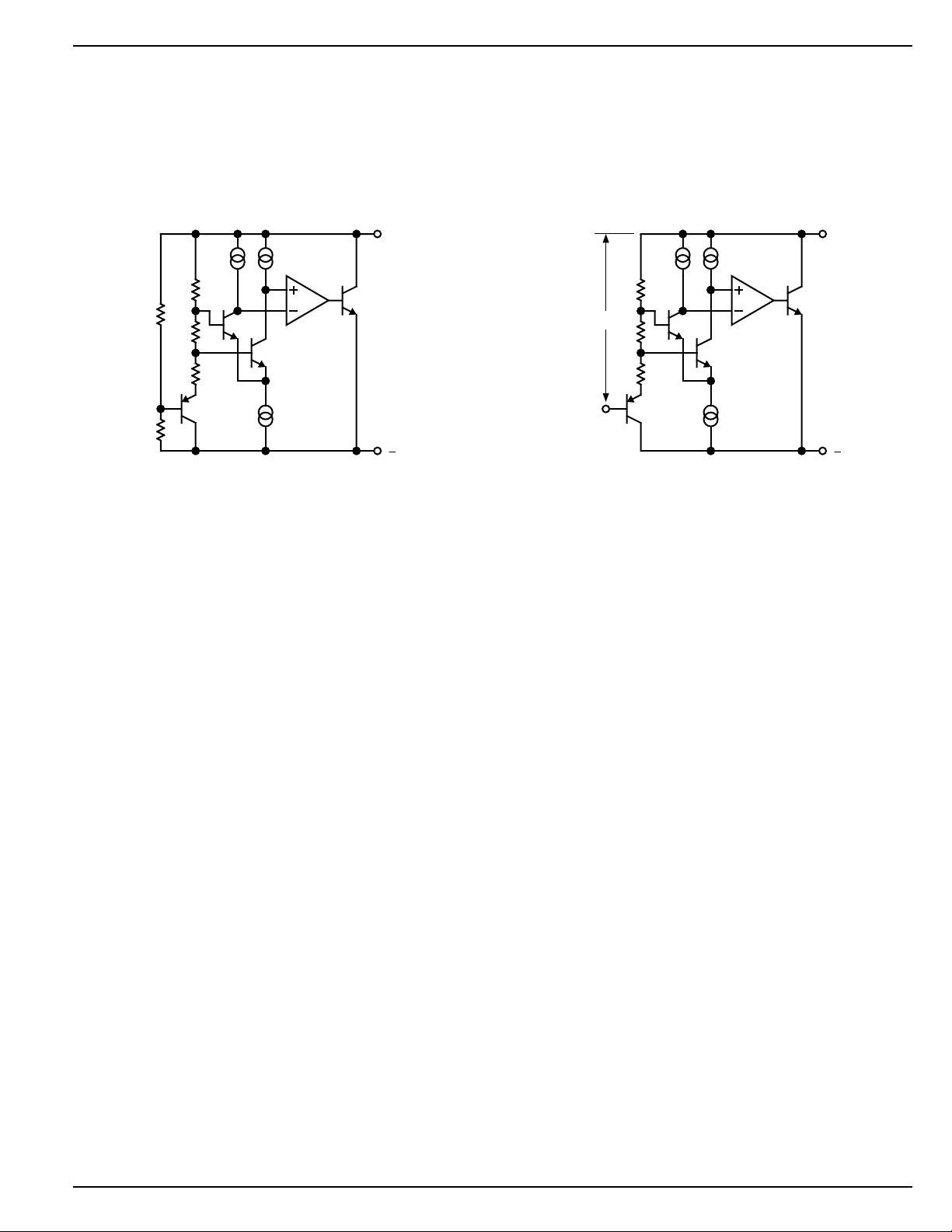
LM4040 T ypical Characteristics
Temperature Drift for Different
Average Temperature Coefficient
+0.5
+0.4
+0.3
+0.2
+0.1
0
-0.1
CHANGE (%)
R
-0.2
V
-0.3
-22ppm/°C
-0.4
-0.5
-40
-200 20406080100
TEMPERATURE (°C)
IR = 150µA
12ppm/°C
-51ppm/°C
Reverse Characteristics and
Minimum Operating Current
120
100
80
60
40
20
REVERSE CURRENT (µA)
0
0 2 4 6 8 10
1k
100
VR = 5V
10
IMPEDANCE (Ω)
1
0.1
100 1k 10k 100k 1M
5V
2.5V
4.1V
Guaranteed
D Suffix
I
RMIN
A, B, C, Suffix
•
•
•
Typical
TJ = 25°C
REVERSE VOLTAGE (V)
Output Impedance
vs. Frequency
IR = I
+ 100 µA
RMIN
= 25 °C, ∆ I
T
J
2.5V
FREQUENCY (Hz)
•
R
= 0.1 I
R
C
= 0
L
C
= 1µF
L
TANTALUM
IMPEDANCE (Ω)
X
CL
Noise Voltage
vs. Frequency
10.0
5.0
2.0
√
1.0
0.5
Noise (µV/ Hz )
0.2
0.1
1 10 100 1k 10k 100k
FREQUENCY (Hz)
Output Impedance
vs. Frequency
1k
100
10
1
0.1
100 1k 10k 100k 1M
IR = 200µA
T
= 25°C
J
5V
2.5V
IR= 1mA
= 25 °C, ∆IR = I
T
J
VR = 5V
2.5V
FREQUENCY (Hz)
CL= 1µF
TANTALUM
R
CL= 0
1Hz rate
LM4040-2.5 RS = 30k
5
(V)
IN
0
6
4
(V) V
R
2
V
0
0 20 40 60 80
RESPONSE TIME (µs)
V
IN
IJ = 25°C
R
S
LM4040
Test Circuit
(V)
V
(V)
R
V
V
R
LM4040-5.0 RS = 30k
10
IN
0
6
4
2
0
0 100 200 300 400
RESPONSE TIME (µs)
TJ = 25°C
January 2000 7 LM4040/4041
Page 8

LM4040/4041 Micrel
LM4041-1.2 Electrical Characteristics
Boldface limits apply for TA = TJ = T
Breakdown Voltage tolerance of ±0.1%, ±0.2%, ±0.5%, and ± 1.0%, respectively.
Symbol Parameter Conditions Typical Units
V
R
Reverse Breakdown Voltage IR = 100µA 1.225 V
Reverse Breakdown Voltage I
Tolerance ±9.2 ±10.4 ±14 mV (max)
I
RMIN
∆V
R
Minimum Operating Current 45 µA
/∆T Average Reverse Breakdown IR = 10mA 20 ppm/°C
Voltage Temperature I
Coefficient IR = 100µA 15 ppm/°C (max)
/∆IRReverse Breakdown Voltage I
∆V
R
Change with Operating 1.5 1.5 1.5 mV (max)
Current Change 2.0 2.0 2.0 mV (max)
Z
e
∆V
R
N
R
Reverse Dynamic Impedance IR = 1mA, f = 120Hz 0.5 Ω
Wideband Noise IR = 100µA
Reverse Breakdown Voltage t = 1000hrs
Long Term Stability T = 25°C ±0.1°C 120 ppm
MIN
to T
; all other limits TA = TJ = 25°C. The grades A, B, C, and D designate initial Reverse
MAX
LM4041AIM3 LM4041BIM3 LM4041CIM3
(Note 4) Limits Limits Limits (Limit)
(Note 5) (Note 5) (Note 5)
= 100µA ±1.2 ±2.4 ±6 mV (max)
R
60 60 60 µA (max)
65 65 65 µA (max)
= 1mA 15 ±100 ±100 ±100 ppm/°C (max)
R
≤ IR 1mA 0.7 mV
RMIN
1mA ≤ I
15mA 4.0 mV
R
6.0 6.0 6.0 mV (max)
8.0 8.0 8.0 mV (max)
IAC = 0.1 I
R
1.5 1.5 1.5 Ω (max)
10Hz ≤ f ≤ 10kHz 20 µV
IR = 100µA
RMS
Symbol Parameter Conditions Typical Units
LM4041DIM3 LM4041EIM3
(Note 4) Limits Limits (Limit)
(Note 5) (Note 5)
V
R
I
RMIN
Reverse Breakdown Voltage IR = 100µA 1.225 V
Reverse Breakdown Voltage I
Tolerance ±24 ±36 mV (max)
= 100µA ±12 ±25 mV (max)
R
Minimum Operating Current 45 µA
65 65 µA (max)
70 70 µA (max)
/∆T Average Reverse Breakdown IR = 10mA 20 ppm/°C
∆V
R
Voltage Temperature I
Coefficient IR = 100µA 15 ppm/°C (max)
/∆IRReverse Breakdown Voltage I
∆V
R
Change with Operating 2.0 2.0 mV (max)
= 1mA 15 ±150 ±150 ppm/°C (max)
R
≤ IR 1mA 0.3 mV
RMIN
Current Change 2.5 2.5 mV (max)
1mA ≤ I
15mA 2.5 mV
R
8.0 8.0 mV (max)
10.0 10.0 mV (max)
Z
e
∆V
R
N
R
Reverse Dynamic Impedance IR = 1mA, f = 120Hz 0.3 Ω
IAC = 0.1 I
R
2.0 2.0 Ω (max)
Wideband Noise IR = 100µA
10Hz ≤ f ≤ 10kHz 35 µV
RMS
Reverse Breakdown Voltage t = 1000hrs
Long Term Stability T = 25°C ±0.1°C 120 ppm
IR = 100µA
LM4040/4041 8 January 2000
Page 9

LM4040/4041 Micrel
LM4041-Adjustable Electrical Characteristics
Boldface limits apply for TA = TJ = T
I
≤ IR < 12mA, V
RMIN
±1%, respectively for V
REF
≤ V
OUT
≤ 10V. The grades C and D designate initial Reverse Breakdown Voltage tolerance of ±0.5% and
OUT
= 5V.
Symbol Parameter Conditions Typical Units
V
REF
Reference Breakdown Voltage IR = 100µA 1.233 V
Reference Breakdown Voltage IR = 100µA ±6.2 ±12 mV (max)
Tolerance (Note 8) ±14 ±24 mV (max)
I
RMIN
∆V
REF
/∆I
R
∆V
REF
/∆V
I
FB
∆V
REF
/∆T Voltage Temperature I
Minimum Operating Current 45 µA
Reference Voltage I
Change with Operating SOT-23: 1.5 2.0 mV (max)
Current Change V
Reference Voltage Change IR = 1mA –1.3 mV/V
with Output Voltage Change –2.0 –2.5 mV/V (max)
O
Feedback Current 60 nA
Average Reference V
Coefficient I
(Note 8) IR = 100µA 15 ppm/°C (max)
Z
e
∆V
OUT
N
REF
Dynamic Output Impedance IR = 1mA, f = 120Hz
Wideband Noise IR = 100µA
Reference Voltage t = 1000hrs
Long Term Stability T = 25°C ±0.1°C 120 ppm
MIN
to T
; all other limits TJ = 25°C unless otherwise specified (SOT-23, see Note 7),
MAX
LM4041CIM3 LM4041DIM3
(Note 4) Limits Limits (Limit)
(Note 5) (Note 5)
V
= 5V
OUT
60 65 µA (max)
65 70 µA (max)
≤ IR 1mA 0.7 mV
RMIN
≥ 1.6V 2.0 2.5 mV (max)
OUT
(Note 7)
1mA ≤ I
SOT-23: 4 6 mV (max)
15mA 2 mV
R
≥ 1.6V 68mV (max)
V
OUT
(Note 7)
–2.5 –3.0 mV/V (max)
100 150 nA (max)
120 200 nA (max)
= 5V
OUT
= 10mA 20 ppm/°C
R
= 1mA 15 ±100 ±150 ppm/°C (max)
R
= 0.1 I
I
AC
R
V
= V
V
OUT
OUT
REF
= 10V 2 Ω (max)
0.3 Ω
10Hz ≤ f ≤ 10kHz 20 µV
IR = 100µA
RMS
January 2000 9 LM4040/4041
Page 10

LM4040/4041 Micrel
LM4040 and LM4041 Electrical Characteristic Notes
Note 1. Absolute Maximum Ratings indicate limits beyond which damage to the device may occur. Operating Ratings indicate conditions for which the
Note 2. The maximum power dissipation must be derated at elevated temperatures and is dictated by T
Note 3. The human body model is a 100pF capacitor discharged through a 1.5kΩ resistor into each pin. The machine model is a 200pF capacitor
Note 4. Typicals are at TJ = 25°C and represent most likely parametric norm.
Note 5. Limits are 100% production tested at 25°C. Limits over temperature are guaranteed through correlation using Statistical Quality Control (SQL)
Note 6. The boldface (over temperature limit for Reverse Breakdown Voltage Tolerance is defined as the room temperature Reverse Breakdown
Note 7. When V
Note 8. Reference voltage and temperature coefficient will change with output voltage. See Typical Performance Characteristics curves.
device is functional, but do not guarantee specific performance limits. For guaranteed specification and test conditions, see the Electrical
Characteristics. The guaranteed specifications apply only for the test conditions listed. Some performance characteristics may degrade when
the device is not operated under the listed test conditions.
(maximum junction temperature), θ
(junction to ambient thermal resistance), and TA (ambient temperature). The maximum allowable power dissipation at any temperature is
= (T
PD
MAX
T
= 125°C, and the typical thermal resistance (θJA), when board mounted, is 326°C/W for the SOT-23 package.
JMAX
– TA)/θJA or the number given in the Absolute Maximum Ratings, whichever is lower. For the LM4040 and LM4041,
JMAX
JMAX
JA
discharged directly into each pin.
methods.
Voltage Tolerance ±[(∆VR/∆T)(65°C)(VR)]. ∆VR/∆T is the VR temperature coefficient, 65°C is the temperature range from –40°C to the
reference point of 25°C, and VR is the reverse breakdown voltage. The total over temperature tolerance for the different grades follows:
A-grade: ±0.75% = ±0.1% ±100ppm/°C × 65°C
B-grade: ±0.85% = ±0.2% ±100ppm/°C × 65°C
C-grade: ±1.15% = ±0.5% ±100ppm/°C × 65°C
D-grade: ±1.98% = ±1.0% ±150ppm/°C × 65°C
Example: The A-grade LM4040-2.5 has an over temperature Reverse Breakdown Voltage tolerance of ±2.5 × 0.75% = ±19mV.
≤ 1.6V, the LM4041-ADJ must operate at reduced IR. This is caused by the series resistance of the die attach between the die (–)
OUT
output and the package (–) output pin. See the Output Saturation curve in the Typical Performance Characteristics section.
LM4041 T ypical Characteristics
Temperature Drift for Different
Average Temperature Coefficient
+0.5
+0.4
+0.3
+0.2
+0.1
0
-0.1
CHANGE (%)
R
-0.2
V
-0.3
-0.4
-0.5
-40
-22ppm/°C
-200 20406080100
TEMPERATURE (°C)
Reverse Characteristics and
Minimum Operating Current
100
80
60
40
20
REVERSE CURRENT (µA)
0
0 0.4 0.8 1.2 1.6 2.0
REVERSE VOLTAGE (V)
LM4041-1.2
12ppm/°C
-51ppm/°C
IR = 150µA
Typical
= 25°C
T
J
LM4041-1.2
Output Impedence
vs. Frequency
1k
100
10
I
R
IMPEDANCE (Ω)
1
I
0.1
100 1k 10k 100k 1M
TJ = 25° C
∆I
LM4041-1.2
= 150µA
= 1mA
R
FREQUENCY (Hz)
R
= 0.1I
R
Reverse Characteristics and
Minimum Operating Current
100
80
60
40
20
REVERSE CURRENT (µA)
0
0 0.4 0.8 1.2 1.6 2.0
REVERSE VOLTAGE (V)
Typical
T
J
LM4041-1.2
CL= 0
CL= 1µF
TANTALUM
X
= 25°C
Voltage Impedance
1000
800
√
600
400
NOISE (nV/ Hz )
200
C
LM4041-ADJ: V
0
1 10 100 1k 10k 100k
FREQUENCY (Hz)
IR = 200µA
TJ = 25°C
LM4041-1.2
= V
OUT
REF
RS 30k
V
1Hz rate
IN
LM4041-1.2
V
R
Test Circuit
LM4040/4041 10 January 2000
Page 11

LM4040/4041 Micrel
T
LM4041 T ypical Characteristics
Reference Voltage vs. Output
Voltage and Temperature
1.244
25°C
1.240
1.236
85°C
-40°C
1.232
1.228
1.224
REFERENCE VOLTAGE (V)
1.220
0 2 4 6 8 10
OUTPUT VOLTAGE (V)
LM4041-ADJ
Output Saturation
1.7
LM4041-ADJ
= V
V
1.6
ADJ
1.5
1.4
1.3
1.2
1.1
OUTPUT SATURATION (V)
1.0
0 2 4 6 8 10 12
+ 5µV
REF
-40°C
25°C
OUTPUT CURRENT (mA)
85°C
85°C
-40°C
Reference Voltage vs.
Temperature and Output Voltage
1.244
LM4041-ADJ
IR = 1mA
1.240
1.236
1.232
V
= V
OUT
REF
V
= 5V
OUT
1.228
V
= 10V
1.224
OUT
REFERENCE VOLTAGE (V)
1.220
-40 -20 0 20 40 60 80 100
TEMPERATURE (°C)
Output Impedence
vs. Frequency *
1K
100
10
V
OUT
IMPEDANCE (Ω)
1
1.23V
0
100 1k 10k 100k 1M
LM4041-ADJ
= 25 °C
T
J
I
= 1mA
R
∆I
= 0.1I
R
= 10V
5V
2.5V
FREQUENCY (Hz)
R
CL = 0
=1µF
C
L
X
C
Feedback Current vs.
Output Voltage and Temperature
100
LM4041-ADJ
80
TJ = 85°C
60
40
FEEDBACK (nA)
20
TJ = 25°C, -40°C
0
0 2 4 6 8 10
OUTPUT VOLTAGE (V)
Output Impedence
vs. Frequency *
1K
100
10
IMPEDANCE (Ω)
1
0
100 1k 10k 100k 1M
LM4041-ADJ
T
V
= 10V
OUT
5V
2.5V
1.23V
FREQUENCY (Hz)
= 25 °C
J
I
= 1mA
R
∆I
= 0.1 I
R
CL = 0
R
=1µF
C
L
X
C
Reverse Characteristics
FB STEPS (V)
0 2 4 6 8
100
80
60
40
20
REVERSE CURRENT (µA)
0
0 2 4 6 8 10
TJ = 25°C
LM4041-ADJ
OUTPUT VOLTAGE (V)
Large Signal Response
-40°C
10
8
6
4
VOLTAGE (V)
2
0
0 10 20 30 40
RESPONSE TIME (µs)
LM4041-ADJ
OUTPUT
INPUT
T
= -40°C
J
-40°C
25°C
85°C
†
I
R
( + )
LM4041-ADJ
FB
( – )
2V / step
V
†
Reverse Characteristics
Test Circuit
V
OU
C
L
* Output Impedance vs. Freq.
Test Circuit
I
R
+
120k
FB
–
‡
+ 15V
5.1k
INPUT
100k
‡
Large Signal Response
FB
( + )
LM4041 - ADJ
( - )
V
OUT
Test Circuit
January 2000 11 LM4040/4041
Page 12

LM4040/4041 Micrel
k
Applications Information
The LM4040 and LM4041 have been designed for stable
operation without the need of an external capacitor connected between the (+) and (–) pins. If a bypass capacitor is
used, the references remain stable.
Schottky Diode
LM4040-x.x and LM4041-1.2 in the SOT-23 package have a
parasitic Schottky diode between pin 2 (–) and pin 3 (die
attach interface connect). Pin 3 of the SOT-23 package must
float or be connected to pin 1. LM4041-ADJs use pin 3 as the
(–) output.
Conventional Shunt Regulator
In a conventional shunt regulator application (see Figure 1),
an external series resistor (RS) is connected between the
supply voltage and the LM4040-x.x or LM4041-1.2 reference.
RS determines the current that flows through the load (IL) and
the reference (IQ). Since load current and supply voltage may
vary, RS should be small enough to supply at least the
minimum acceptable IQ to the reference even when the
supply voltage is at its minimum and the load current is at its
maximum value. When the supply voltage is at its maximum
and IL is at its minimum, RS should be large enough so that
the current flowing through the LM4040-x.x is less than
15mA, and the current flowing through the LM4041-1.2 or
LM4041-ADJ is less than 12mA.
RS is determined by the supply voltage (VS), the load and
operating current, (IL and IQ), and the reference’s reverse
breakdown voltage (VR).
Rs = (Vs – VR) / (IL + IQ)
Adjustable Regulator
The LM4041-ADJ’s output voltage can be adjusted to any
value in the range of 1.24V through 10V. It is a function of the
internal reference voltage (V
) and the ratio of the external
REF
feedback resistors as shown in Figure 2. The output is found
using the equation
(1) VO = V
´ [ (R2/R1) + 1 ]
REF
where VO is the desired output voltage. The actual value of
the internal V
is a function of VO. The “corrected” V
REF
REF
is
determined by
(2) V
where VO is the desired output voltage. ∆V
´ = VO (∆V
REF
/ ∆VO) + V
REF
Y
/ ∆VO is found
REF
in the Electrical Characteristics and is typically –1.3mV/V and
VY is equal to 1.233V. Replace the value of V
´ in equation
REF
(1) with the value found using equation (2).
Note that actual output voltage can deviate from that pre-
dicted using the typical ∆V
grade parts, the worst-case ∆V
/ ∆VO in equation (2); for C-
REF
/ ∆VO is –2.5mV/V and
REF
VY = 1.248V.
The following example shows the difference in output voltage
resulting from the typical and worst case values of
∆V
/ ∆VO:
REF
Let VO = +9V. Using the typical values of ∆V
REF
/∆VO , V
REF
is 1.223V. Choosing a value of R1 = 10kΩ, R2 = 63.272kΩ.
Using the worst case ∆V
/ ∆VO for the C-grade and D-
REF
grade parts, the output voltage is actually 8.965V and 8.946V
respectively. This results in possible errors as large as 0.39%
for the C-grade parts and 0.59% for the D-grade parts. Once
again, resistor values found using the typical value of
∆V
/ ∆VO will work in most cases, requiring no further
REF
adjustment.
FB
λ
R1
120
R2
1M
< –12V
LED ON
LM4041-ADJ
D1
+
–
R3
200
–5V
Figure 3. Voltage Level Detector
ADJ
+
–
R3
330
–5V
λ
D1
LM4041-
Figure 4. Voltage Level Detector
FB
R1
120k
R2
1M
> –12V
LED ON
LM4040/4041 12 January 2000
Page 13

LM4040/4041 Micrel
V
IN
R1I
LM4041-ADJ
D2
1N457
R3
1M
R2
330k
V
OUT
LM4041-ADJ
FB
+
–
FB
–
+
D1
1N457
R4
330k
V
IN
R1
I
V
R2
50µA
LM4041-ADJ
D1
1N914
+
FB
–
OUT
D2
1N914
R3
240k
R4
240k
LM4041-ADJ
+
FB
–
D1
1N457
V
IN
I
R1
V
R2
510k
R3
FB
–
+
OUT
D2
1N457
LM4041-ADJ
510k
Figure 5. Fast Positive Clamp
LM4041-ADJ
2.4V + ∆V
R3
500k
+
FB
–
D1
1N457
I
D1
V
IN
R1
R2
390k
R4
390k
FB
–
+
Figure 7. Bidirectional Adjustable Clamp
±18V to ±2.4V
0 to 20mA
R1
390Ω
1N4002
± 2%
D2
D1* 1
V
OUT
D2
1N457
LM4041-ADJ
FB
λ
+
LM4041-ADJ
–
Figure 6. Bidirectional Clamp
±2.4V
Figure 8. Bidirectional Adjustable Clamp
±2.4 to ±6V
+ 5V
R2
6
470k
N.C.
January 2000 13 LM4040/4041
I
THRESHOLD
2
3
N.C.
=
1.24V
R1
5µA
+
4N28 GAIN
4N28
= 3.2mA
5
CMOS
4
Figure 9. Floating Current Detector
Page 14

LM4040/4041 Micrel
+15V
0 to 20 mA
D2
1N4002
+
LM4041-ADJ
–
R2
120k
1µA < I
OUT
I
Figure 10. Current Source
R1
332Ω
±1%
1N914
2N2222
R2
22k
FB
+
LM4041-ADJ
–
1
FB
2N
3964
= 100mA
1.24V
=
OUT
R1
2N2905
R1
+5V
R3
100k
6
D1*
N.C.
2
3
4N28
I
THRESHOLD
1.24V
=
R1
λ
= 3.7mA ± 2%
Figure 11. Precision Floating Current Detector
* D1 can be any LED, VF = 1.5V to 2.2V at 3mA. D1 may act as an indicator. D1 will
be on if I
THRESHOLD
falls below the threshold current, except with I = O.
5
CMOS
R4
4
10M
LM4040/4041 14 January 2000
Page 15

LM4040/4041 Micrel
Package Information
C
L
2.36 (0.093)
2.28 (0.090)
3.05 (0.120)
2.67 (0.105)
0.445 (0.0175) TYP 3 PLACES
1.40 (0.055)
1.19 (0.047)
C
L
1.15 (0.045)
0.76 (0.030)
0.10 (0.004)
0.013 (0.0005)
2.50 (0.098)
2.10 (0.083)
8°
0°
DIMENSIONS:
MM (INCH)
0.15 (0.006)
0.076 (0.0030)
0.41 (0.016)
0.13 (0.005)
SOT-23 (M3)
January 2000 15 LM4040/4041
Page 16

LM4040/4041 Micrel
MICREL INC. 1849 FORTUNE DRIVE SAN JOSE, CA 95131 USA
TEL + 1 (408) 944-0800 FAX + 1 (408) 944-0970 WEB http://www.micrel.com
This information is believed to be accurate and reliable, however no responsibility is assumed by Micrel for its use nor for any infringement of patents or
other rights of third parties resulting from its use. No license is granted by implication or otherwise under any patent or patent right of Micrel Inc.
© 2000 Micrel Incorporated
LM4040/4041 16 January 2000
 Loading...