

Datasheet LM4040EIM3-2.5, LM4040EEM3X-2.5, LM4040EEM3-2.5, LM4040DIZ-8.2, LM4040DIZ-4.1 Datasheet (NSC)
...Page 1
LM4040
Precision Micropower Shunt Voltage Reference
General Description
Ideal for space critical applications, the LM4040 precision
voltage reference is available in the sub-miniature (3 mm x
1.3 mm) SOT-23 surface-mountpackage.The LM4040’s advanced design eliminates the need for an external stabilizing
capacitor while ensuring stability with any capacitive load,
thus making the LM4040 easy to use. Further reducing design effort is the availability of several fixed reverse breakdown voltages: 2.500V, 4.096V, 5.000V, 8.192V, and
10.000V. The minimum operating current increases from
60 µA for the LM4040-2.5 to 100 µA for the LM4040-10.0. All
versions have a maximum operating current of 15 mA.
The LM4040 utilizes fuse and zener-zap reverse breakdown
voltage trim during wafer sort to ensure that the prime parts
have an accuracy of better than
±
0.1%(A grade) at 25˚C.
Bandgap reference temperature drift curvature correction
and low dynamic impedance ensure stable reverse breakdown voltage accuracy over a wide range of operating temperatures and currents.
Also available is the LM4041 with two reverse breakdown
voltage versions: adjustable and 1.2V. Please see the
LM4041 data sheet.
Features
n Small packages: SOT-23, TO-92
n No output capacitor required
n Tolerates capacitive loads
n Fixed reverse breakdown voltages of 2.500V, 4.096V,
5.000V, 8.192V, and 10.000V
Key Specifications (LM4040-2.5)
n Output voltage tolerance
(A grade, 25˚C)
±
0.1%(max)
n Low output noise
(10 Hz to 10 kHz) 35 µV
rms
(typ)
n Wide operating current range 60 µA to 15 mA
n Industrial temperature range −40˚C to +85˚C
n Extended temperature range −40˚C to +125˚C
n Low temperature coefficient 100 ppm/˚C (max)
Applications
n Portable, Battery-Powered Equipment
n Data Acquisition Systems
n Instrumentation
n Process Control
n Energy Management
n Product Testing
n Automotive
n Precision Audio Components
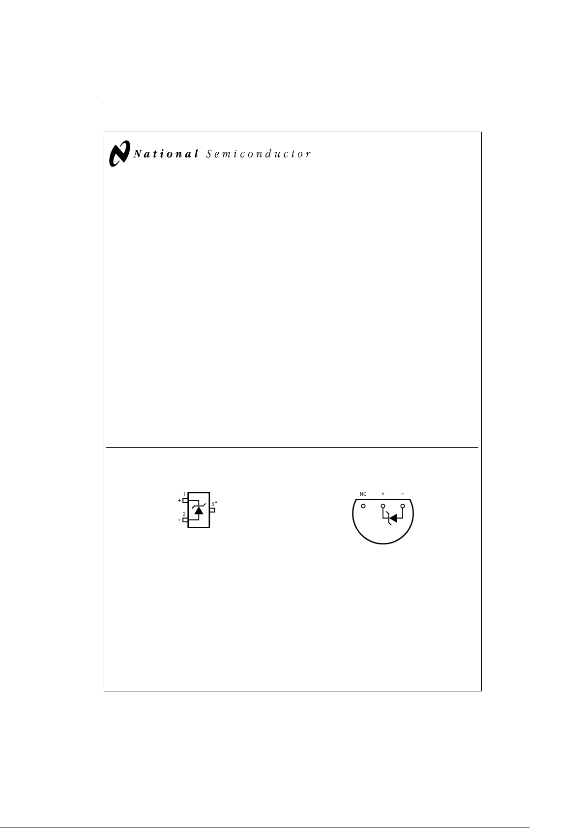
Connection Diagrams
SOT-23
DS011323-1
*This pin must be left floating or connected to pin 2.
Top View
See NS Package Number M03B
(JEDEC Registration TO-236AB)
TO-92
DS011323-3
Bottom View
See NS Package Number Z03A
September 1998
LM4040 Precision Micropower Shunt Voltage Reference
© 1998 National Semiconductor Corporation DS011323 www.national.com
Page 2

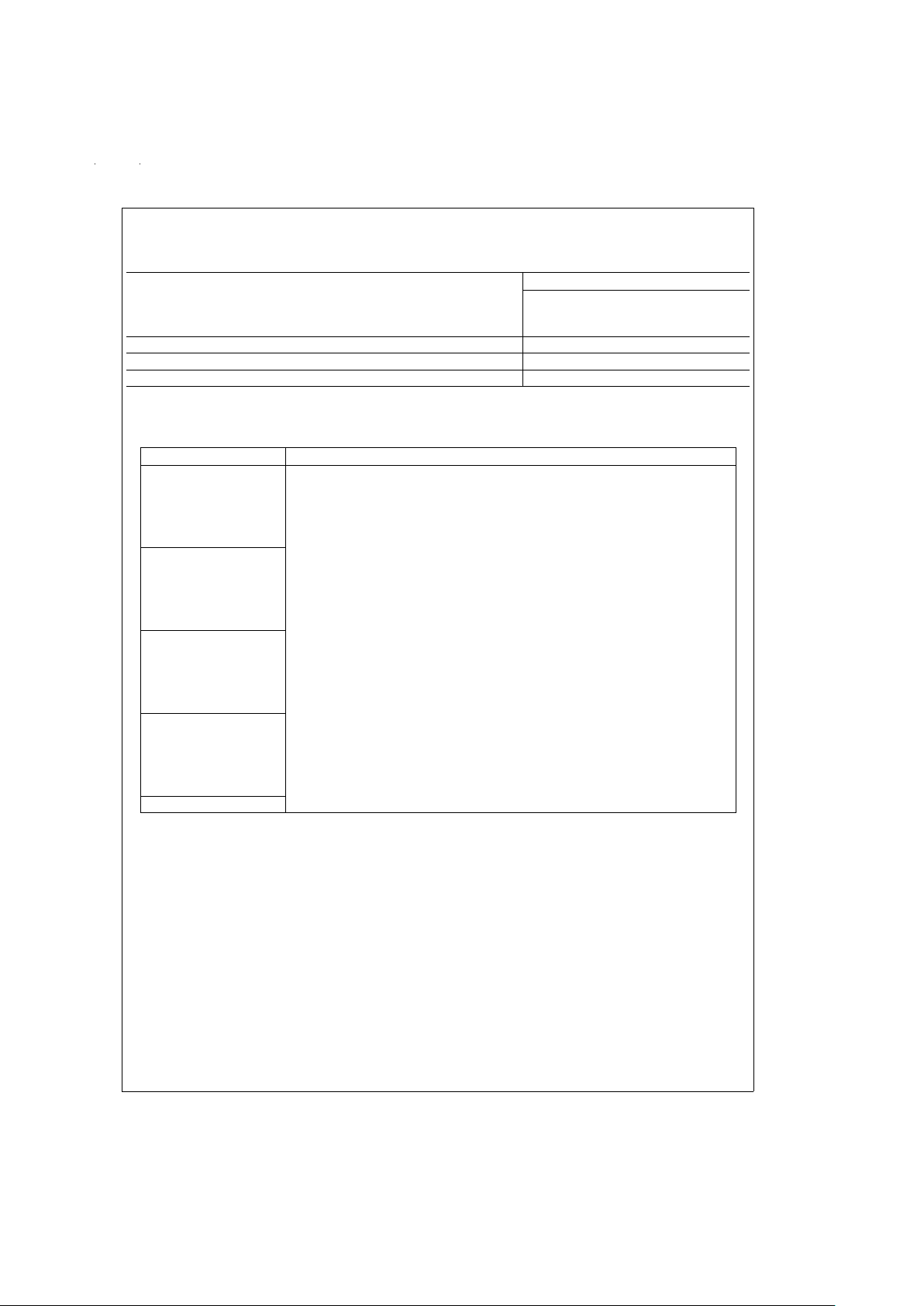
Ordering Information
Industrial Temperature Range (−40 ˚C to +85 ˚C)
Reverse Breakdown
Voltage Tolerance at 25˚C
and Average Reverse Breakdown
Voltage Temperature Coefficient
Package
M3 (SOT-23) Z (TO-92)
±
0.1%, 100 ppm/˚C max (A grade) LM4040AIM3-2.5, LM4040AIZ-2.5,
LM4040AIM3-4.1, LM4040AIZ-4.1,
LM4040AIM3-5.0, LM4040AIZ-5.0,
LM4040AIM3-8.2, LM4040AIZ-8.2,
LM4040AIM3-10.0 LM4040AIZ-10.0
See NS Package See NS Package
Number M03B Number Z03A
±
0.2%, 100 ppm/˚C max (B grade) LM4040BIM3-2.5, LM4040BIZ-2.5,
LM4040BIM3-4.1, LM4040BIZ-4.1,
LM4040BIM3-5.0, LM4040BIZ-5.0,
LM4040BIM3-8.2, LM4040BIZ-8.2,
LM4040BIM3-10.0 LM4040BIZ-10.0
See NS Package See NS Package
Number M03B Number Z03A
±
0.5%, 100 ppm/˚C max (C grade) LM4040CIM3-2.5, LM4040CIZ-2.5,
LM4040CIM3-4.1, LM4040CIZ-4.1,
LM4040CIM3-5.0, LM4040CIZ-5.0,
LM4040CIM3-8.2, LM4040CIZ-8.2,
LM4040CIM3-10.0 LM4040CIZ-10.0
See NS Package See NS Package
Number M03B Number Z03A
±
1.0%, 150 ppm/˚C max (D grade) LM4040DIM3-2.5, LM4040DIZ-2.5,
LM4040DIM3-4.1, LM4040DIZ-4.1,
LM4040DIM3-5.0, LM4040DIZ-5.0,
LM4040DIM3-8.2, LM4040DIZ-10.0,
LM4040DIM3-10.0
See NS Package See NS Package
Number M03B Number Z03A
±
2.0%, 150 ppm/˚C max (E grade) LM4040EIM3-2.5 LM4040EIZ-2.5
See NS Package See NS Package
Number M03B Number Z03A
www.national.com 2
Page 3
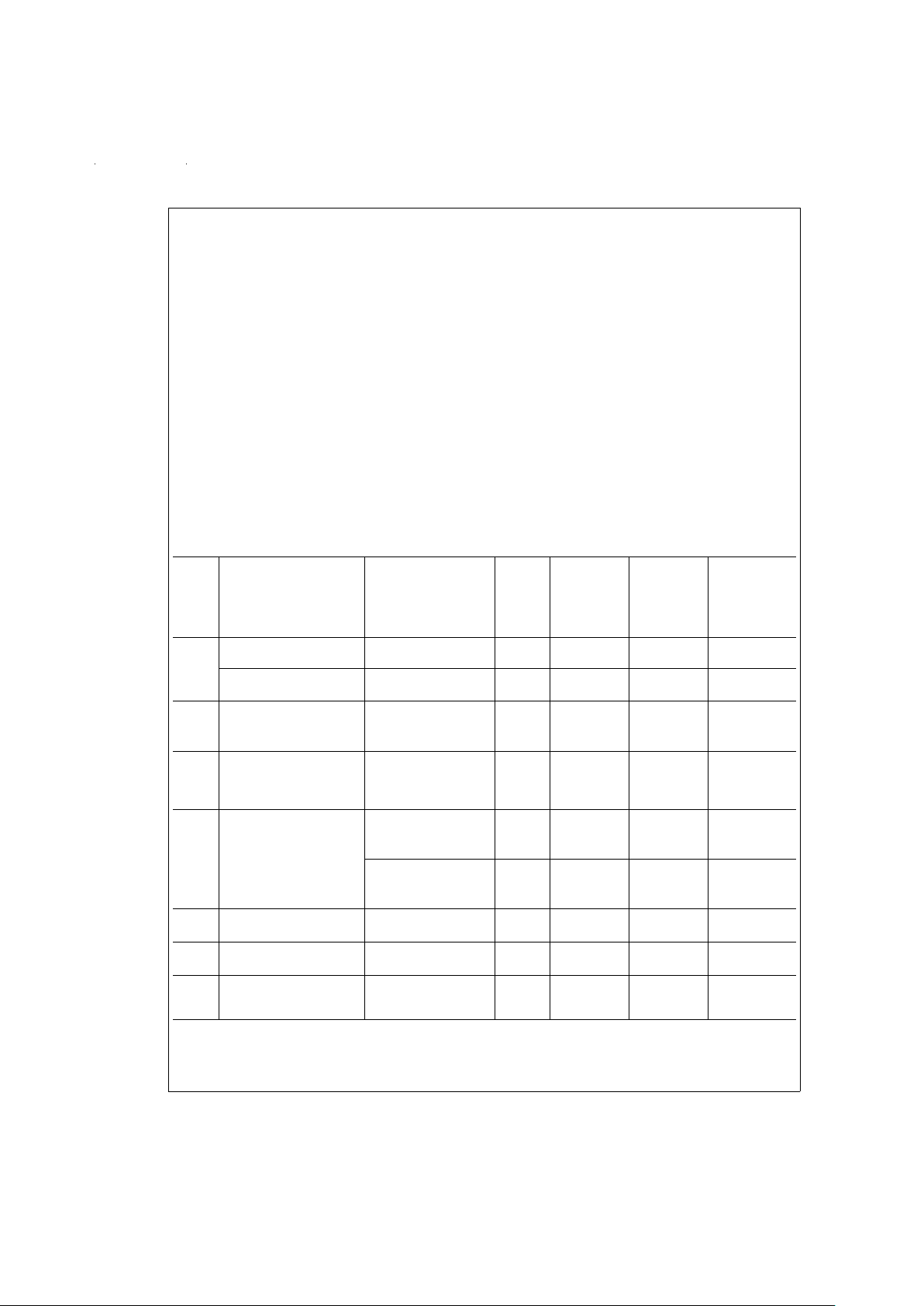
Ordering Information (Continued)
Extended Temperature Range (−40 ˚C to +125 ˚C)
Reverse Breakdown
Voltage Tolerance at 25 ˚C
and Average Reverse Breakdown
Voltage Temperature Coefficient
Package
M3 (SOT-23)
See NS Package
Number M03B
±
0.5%, 100 ppm/˚C max (C grade) LM4040CEM3-2.5, LM4040CEM3-5.0
±
1.0%, 150 ppm/˚C max (D grade) LM4040DEM3-2.5, LM4040DEM3-5.0
±
2.0%, 150 ppm/˚C max (E grade) LM4040EEM3-2.5
SOT-23 Package Marking Information
Only three fields of marking are possible on the SOT-23’s small surface. This table gives the meaning of the three fields.
Part Marking Field Definition
R2A First Field:
R4A R=Reference
R5A Second Field:
R8A 2=2.500V Voltage Option
R0A 4=4.096V Voltage Option
R2B 5=5.000V Voltage Option
R4B 8=8.192V Voltage Option
R5B 0=10.000V Voltage Option
R8B
R0B Third Field:
R2C A–E=Initial Reverse Breakdown Voltage or Reference Voltage Tolerance
R4C A
=
±
0.1%,B
=
±
0.2%,C=+0.5%,D
=
±
1.0%,E
=
±
2.0
%
R5C
R8C
R0C
R2D
R4D
R5D
R8D
R0D
R2E
www.national.com3
Page 4
Absolute Maximum Ratings (Note 1)
If Military/Aerospace specified devices are required,
please contact the National Semiconductor Sales Office/
Distributors for availability and specifications.
Reverse Current 20 mA
Forward Current 10 mA
Power Dissipation (T
A
=
25˚C) (Note 2)
M3 Package 306 mW
Z Package 550 mW
Storage Temperature −65˚C to +150˚C
Lead Temperature
M3 Package
Vapor phase (60 seconds) +215˚C
Infrared (15 seconds) +220˚C
Z Package
Soldering (10 seconds) +260˚C
ESD Susceptibility
Human Body Model (Note 3) 2 kV
Machine Model (Note 3) 200V
See AN-450 “Surface Mounting Methods and Their Effect
on Product Reliability” for other methods of soldering
surface mount devices.
Operating Ratings(Notes 1, 2)
Temperature Range (T
min
≤ TA≤ T
max
)
Industrial Temperature Range −40˚C ≤ T
A
≤ +85˚C
Extended Temperature Range −40˚C ≤ T
A
≤ +125˚C
Reverse Current
LM4040-2.5 60 µA to 15 mA
LM4040-4.1 68 µA to 15 mA
LM4040-5.0 74 µA to 15 mA
LM4040-8.2 91 µA to 15 mA
LM4040-10.0 100 µA to 15 mA
LM4040-2.5
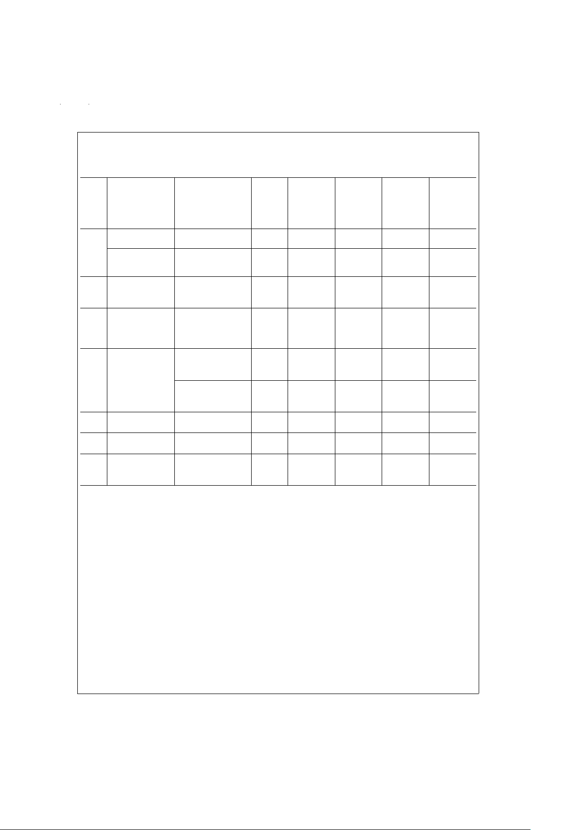
Electrical Characteristics (Industrial Temperature Range)
Boldface limits apply for T
A
=
T
J
=
T
MIN
to T
MAX
; all other limits T
A
=
T
J
=
25˚C. The grades A and B designate initial Re-
verse Breakdown Voltage tolerances of
±
0.1%and±0.2%, respectively.
Typical LM4040AIM3 LM4040BIM3 Units
Symbol Parameter Conditions (Note 4) LM4040AIZ LM4040BIZ (Limit)
Limits Limits
(Note 5) (Note 5)
V
R
Reverse Breakdown
Voltage
I
R
=
100 µA 2.500 V
Reverse Breakdown
Voltage Tolerance (Note 6)
I
R
=
100 µA
±
2.5
±
5.0 mV (max)
±
19
±
21 mV (max)
I
RMIN
Minimum Operating Current 45 µA
60 60 µA (max)
65 65 µA (max)
∆V
R
/∆T Average Reverse
Breakdown Voltage
Temperature Coefficient
(Note 6)
I
R
=
10 mA
±
20 ppm/˚C
I
R
=
1mA
±
15
±
100
±
100 ppm/˚C (max)
I
R
=
100 µA
±
15 ppm/˚C
∆V
R
/∆IRReverse Breakdown
Voltage Change with
Operating Current Change
I
RMIN
≤ IR≤ 1 mA 0.3 mV
0.8 0.8 mV (max)
1.0 1.0 mV (max)
1mA≤I
R
≤15 mA 2.5 mV
6.0 6.0 mV (max)
8.0 8.0 mV (max)
Z
R
Reverse Dynamic
Impedance
I
R
=
1 mA, f=120 Hz,
I
AC
=
0.1 I
R
0.3 Ω
0.8 0.8 Ω (max)
e
N
Wideband Noise I
R
=
100 µA 35 µV
rms
10 Hz ≤ f ≤ 10 kHz
∆V
R
Reverse Breakdown
Voltage Long Term Stability
t=1000 hrs
T=25˚C
±
0.1˚C
I
R
=
100 µA
120 ppm
www.national.com 4
Page 5
LM4040-2.5
Electrical Characteristics (Industrial Temperature Range)
Boldface limits apply for T
A
=
T
J
=
T
MIN
to T
MAX
; all other limits T
A
=
T
J
=
25˚C. The grades C, D and E designate initial
Reverse Breakdown Voltage tolerances of
±
0.5%,±1.0%and±2.0%, respectively.
Typical
(Note 4)
LM4040CIM3 LM4040DIM3 LM4040EIZ
Units
(Limit)
Symbol Parameter Conditions LM4040CIZ LM4040DIZ
Limits Limits Limits
(Note 5) (Note 5) (Note 5)
V
R
Reverse
Breakdown Voltage
I
R
=
100 µA 2.500 V
Reverse
Breakdown Voltage
Tolerance (Note 6)
I
R
=
100 µA
±
12
±
25
±
50 mV (max)
±
29
±
49
±
74 mV (max)
I
RMIN
Minimum Operating
Current
45 µA
60 65 65 µA (max)
65 70 70 µA (max)
∆V
R
/∆T Average Reverse
Breakdown Voltage
Temperature
Coefficient(Note 6)
I
R
=
10 mA
±
20 ppm/˚C
I
R
=
1mA
±
15
±
100
±
150
±
150 ppm/˚C
(max)
I
R
=
100 µA
±
15 ppm/˚C
∆V
R
/∆IRReverse
Breakdown Voltage
Change with
Operating Current
Change
I
RMIN
≤ IR≤ 1 mA 0.4 mV
0.8 1.0 1.0 mV (max)
1.0 1.2 1.2 mV (max)
1mA≤I
R
≤15 mA 2.5 mV
6.0 8.0 8.0 mV (max)
8.0 10.0 10.0 mV (max)
Z
R
Reverse Dynamic
Impedance
I
R
=
1 mA, f=120 Hz 0.3 Ω
I
AC
=
0.1 I
R
0.9 1.1 1.1 Ω(max)
e
N
Wideband Noise I
R
=
100 µA 35 µV
rms
10 Hz ≤ f ≤ 10 kHz
∆V
R
Reverse
Breakdown Voltage
Long Term Stability
t=1000 hrs
T=25˚C
±
0.1˚C 120 ppm
I
R
=
100 µA
www.national.com5
Page 6
LM4040-2.5
Electrical Characteristics (Extended Temperature Range)
Boldface limits apply for T
A
=
T
J
=
T
MIN
to T
MAX
; all other limits T
A
=
T
J
=
25˚C. The grades C, D and E designate initial
Reverse Breakdown Voltage tolerances of
±
0.5
,±1.0%and±2.0%,respectively.
Symbol Parameter Conditions Typical LM4040CEM3 LM4040DEM3 LM4040EEM3 Units
Limits Limits Limits (Limit)
(Note 4) (Note 5) (Note 5) (Note 5)
V
R
Reverse
Breakdown Voltage
I
R
=
100 µA 2.500 V
Reverse
Breakdown Voltage
Tolerance(Note 6)
I
R
=
100 µA
±
12
±
25
±
50 mV (max)
±
38
±
63
±
88 mV (max)
I
RMIN
Minimum Operating
Current
45 µA
60 60 60 µA (max)
68 73 73 µA (max)
∆V
R
/∆T Average Reverse
Breakdown Voltage
Temperature
Coefficient (Note 6)
I
R
=
10 mA
±
20 ppm/˚C
I
R
=
1mA
±
15
±
100
±
150
±
150 ppm/˚C (max)
I
R
=
100 µA
±
15 ppm/˚C
∆V
R
/∆IRReverse
Breakdown Voltage
Change with
Operating Current
Change
I
RMIN
≤ IR≤ 1 mA 0.3 mV
0.8 1.0 1.0 mV (max)
1.0 1.2 1.2 mV (max)
1mA≤I
R
≤15 mA 2.5 mV
6.0 8.0 8.0 mV (max)
8.0 10.0 10.0 mV (max)
Z
R
Reverse Dynamic
Impedance
I
R
=
1 mA, f=120
Hz, I
AC
=
0.1 I
R
0.3 Ω
0.9 1.1 1.1 Ω (max)
e
N
Wideband Noise I
R
=
100 µA 35 µV
rms
10 Hz ≤ f ≤ 10 kHz
∆V
R
Reverse
Breakdown Voltage
Long Term Stability
t=1000 hrs
T=25˚C
±
0.1˚C
I
R
=
100 µA
120 ppm
www.national.com 6
Page 7
LM4040-4.1
Electrical Characteristics (Industrial Temperature Range)
Boldface limits apply for T
A
=
T
J
=
T
MIN
to T
MAX
; all other limits T
A
=
T
J
=
25˚C. The grades A and B designate initial Re-
verse Breakdown Voltage tolerances of
±
0.1%and±0.2%, respectively.
Symbol Parameter Conditions
Typical
(Note 4)
Units
(Limit)
LM4040AIM3 LM4040BIM3
LM4040AIZ LM4040BIZ
Limits Limits
(Note 5) (Note 5)
V
R
Reverse Breakdown
Voltage
I
R
=
100 µA 4.096 V
Reverse Breakdown
Voltage Tolerance (Note 6)
I
R
=
100 µA
±
4.1
±
8.2 mV (max)
±
31
±
35 mV (max)
I
RMIN
Minimum Operating Current 50 µA
68 68 µA (max)
73 73 µA (max)
∆V
R
/∆T Average Reverse
Breakdown Voltage
Temperature
Coefficient(Note 6)
I
R
=
10 mA
±
30 ppm/˚C
I
R
=
1mA
±
20
±
100
±
100 ppm/˚C (max)
I
R
=
100 µA
±
20 ppm/˚C
∆V
R
/∆IRReverse Breakdown
Voltage Change with
Operating Current Change
I
RMIN
≤ IR≤ 1 mA 0.5 mV
0.9 0.9 mV (max)
1.2 1.2 mV (max)
1mA≤I
R
≤15 mA 3.0 mV
7.0 7.0 mV (max)
10.0 10.0 mV (max)
Z
R
Reverse Dynamic
Impedance
I
R
=
1 mA, f=120 Hz, 0.5 Ω
I
AC
=
0.1 I
R
1.0 1.0 Ω (max)
e
N
Wideband Noise I
R
=
100 µA 80 µV
rms
10 Hz ≤ f ≤ 10 kHz
∆V
R
Reverse Breakdown
Voltage Long Term Stability
t=1000 hrs
T=25˚C
±
0.1˚C
I
R
=
100 µA
120 ppm
www.national.com7
Page 8
LM4040-4.1
Electrical Characteristics (Industrial Temperature Range)
Boldface limits apply for T
A
=
T
J
=
T
MIN
to T
MAX
; all other limits T
A
=
T
J
=
25˚C. The grades C and D designate initial Re-
verse Breakdown Voltage tolerances of
±
0.5%and±1.0%, respectively.
Symbol Parameter Conditions
Typical
(Note 4)
Units
(Limit)
LM4040CIM3 LM4040DIM3
LM4040CIZ LM4040DIZ
Limits Limits
(Note 5) (Note 5)
V
R
Reverse Breakdown
Voltage
I
R
=
100 µA 4.096 V
Reverse Breakdown
Voltage Tolerance (Note 6)
I
R
=
100 µA
±
20
±
41 mV (max)
±
47
±
81 mV (max)
I
RMIN
Minimum Operating Current 50 µA
68 73 µA (max)
73 78 µA (max)
∆V
R
/∆T Average Reverse
Breakdown Voltage
Temperature Coefficient
(Note 6)
I
R
=
10 mA
±
30 ppm/˚C
I
R
=
1mA
±
20
±
100
±
150 ppm/˚C (max)
I
R
=
100 µA
±
20 ppm/˚C
∆V
R
/∆IRReverse Breakdown
Voltage Change with
Operating Current Change
I
RMIN
≤ IR≤ 1 mA 0.5 mV
0.9 1.2 mV (max)
1.2 1.5 mV (max)
1mA≤I
R
≤15 mA 3.0 mV
7.0 9.0 mV (max)
10.0 13.0 mV (max)
Z
R
Reverse Dynamic
Impedance
I
R
=
1 mA, f=120 Hz, 0.5 Ω
I
AC
=
0.1 I
R
1.0 1.3 Ω (max)
e
N
Wideband Noise I
R
=
100 µA 80 µV
rms
10 Hz ≤ f ≤ 10 kHz
∆V
R
Reverse Breakdown
Voltage Long Term Stability
t=1000 hrs
T=25˚C
±
0.1˚C
I
R
=
100 µA
120 ppm
www.national.com 8
Page 9

LM4040-5.0
Electrical Characteristics (Industrial Temperature Range)
Boldface limits apply for T
A
=
T
J
=
T
MIN
to T
MAX
; all other limits T
A
=
T
J
=
25˚C. The grades A and B designate initial Re-
verse Breakdown Voltage tolerances of
±
0.1%and±0.2%, respectively.
Symbol Parameter Conditions
Typical
(Note 4)
Units
(Limit)
LM4040AIM3 LM4040BIM3
LM4040AIZ LM4040BIZ
Limits Limits
(Note 5) (Note 5)
V
R
Reverse Breakdown
Voltage
I
R
=
100 µA 5.000 V
Reverse Breakdown
Voltage Tolerance (Note 6)
I
R
=
100 µA
±
5.0
±
10 mV (max)
±
38
±
43 mV (max)
I
RMIN
Minimum Operating Current 54 µA
74 74 µA (max)
80 80 µA (max)
∆V
R
/∆T Average Reverse
Breakdown Voltage
Temperature Coefficient
(Note 6)
I
R
=
10 mA
±
30 ppm/˚C
I
R
=
1mA
±
20
±
100
±
100 ppm/˚C (max)
I
R
=
100 µA
±
20 ppm/˚C
∆V
R
/∆IRReverse Breakdown
Voltage Change with
Operating Current Change
I
RMIN
≤ IR≤ 1 mA 0.5 mV
1.0 1.0 mV (max)
1.4 1.4 mV (max)
1mA≤I
R
≤15 mA 3.5 mV
8.0 8.0 mV (max)
12.0 12.0 mV (max)
Z
R
Reverse Dynamic
Impedance
I
R
=
1 mA, f=120 Hz, 0.5 Ω
I
AC
=
0.1 I
R
1.1 1.1 Ω (max)
e
N
Wideband Noise I
R
=
100 µA 80 µV
rms
10 Hz ≤ f ≤ 10 kHz
∆V
R
Reverse Breakdown
Voltage Long Term Stability
t=1000 hrs
T=25˚C
±
0.1˚C 120 ppm
I
R
=
100 µA
www.national.com9
Page 10

LM4040-5.0
Electrical Characteristics (Industrial Temperature Range)
Boldface limits apply for T
A
=
T
J
=
T
MIN
to T
MAX
; all other limits T
A
=
T
J
=
25˚C. The grades C and D designate initial Re-
verse Breakdown Voltage tolerances of
±
0.5%and±1.0%, respectively.
Symbol Parameter Conditions
Typical
(Note 4)
Units
(Limit)
LM4040CIM3 LM4040DIM3
LM4040CIZ LM4040DIZ
Limits Limits
(Note 5) (Note 5)
V
R
Reverse Breakdown
Voltage
I
R
=
100 µA 5.000 V
Reverse Breakdown
Voltage Tolerance (Note 6)
I
R
=
100 µA
±
25
±
50 mV (max)
±
58
±
99 mV (max)
I
RMIN
Minimum Operating Current 54 µA
74 79 µA (max)
80 85 µA (max)
∆V
R
/∆T Average Reverse
Breakdown Voltage
Temperature Coefficient
(Note 6)
I
R
=
10 mA
±
30 ppm/˚C
I
R
=
1mA
±
20
±
100
±
150 ppm/˚C (max)
I
R
=
100 µA
±
20 ppm/˚C
∆V
R
/∆IRReverse Breakdown
Voltage Change with
Operating Current Change
I
RMIN
≤ IR≤ 1 mA 0.5 mV
1.0 1.3 mV (max)
1.4 1.8 mV (max)
1mA≤I
R
≤15 mA 3.5 mV
8.0 10.0 mV (max)
12.0 15.0 mV (max)
Z
R
Reverse Dynamic
Impedance
I
R
=
1 mA, f=120 Hz, 0.5 Ω
I
AC
=
0.1 I
R
1.1 1.5 Ω (max)
e
N
Wideband Noise I
R
=
100 µA 80 µV
rms
10 Hz ≤ f ≤ 10 kHz
∆V
R
Reverse Breakdown
Voltage Long Term Stability
t=1000 hrs
T=25˚C
±
0.1˚C 120 ppm
I
R
=
100 µA
www.national.com 10
Page 11

LM4040-5.0
Electrical Characteristics (Extended Temperature Range)
Boldface limits apply for T
A
=
T
J
=
T
MIN
to T
MAX
; all other limits T
A
=
T
J
=
25˚C. The grades C and D designate initial Re-
verse Breakdown Voltage tolerances of
±
0.5%and±1.0%, respectively.
Symbol Parameter Conditions Typical LM4040CEM3 LM4040DEM3 Units
Limits Limits (Limit)
(Note 4) (Note 5) (Note 5)
V
R
Reverse Breakdown
Voltage
I
R
=
100 µA 5.000 V
Reverse Breakdown
Voltage Tolerance(Note 6)
I
R
=
100 µA
±
25
±
50 mV (max)
±
75
±
125 mV (max)
I
RMIN
Minimum Operating
Current
54 µA
74 79 µA (max)
83 88 µA (max)
∆V
R
/∆T Average Reverse
Breakdown Voltage
Temperature Coefficient
(Note 6)
I
R
=
10 mA
±
30 ppm/˚C
I
R
=
1mA
±
20
±
100
±
150 ppm/˚C (max)
I
R
=
100 µA
±
20 ppm/˚C
∆V
R
/∆IRReverse Breakdown
Voltage Change with
Operating Current Change
I
RMIN
≤ IR≤ 1 mA 0.5 mV
1.0 1.0 mV (max)
1.4 1.8 mV (max)
1mA≤I
R
≤15 mA 3.5 mV
8.0 8.0 mV (max)
12.0 15.0 mV (max)
Z
R
Reverse Dynamic
Impedance
I
R
=
1 mA, f=120 Hz, I
AC
=
0.1 I
R
0.5 Ω
1.1 1.1 Ω (max)
e
N
Wideband Noise I
R
=
100 µA 80 µV
rms
10 Hz ≤ f ≤ 10 kHz
∆V
R
Reverse Breakdown
Voltage Long Term
Stability
t=1000 hrs
T=25˚C
±
0.1˚C
I
R
=
100 µA
120 ppm
www.national.com11
Page 12

LM4040-8.2
Electrical Characteristics (Industrial Temperature Range)
Boldface limits apply for T
A
=
T
J
=
T
MIN
to T
MAX
; all other limits T
A
=
T
J
=
25˚C. The grades A and B designate initial Re-
verse Breakdown Voltage tolerances of
±
0.1%and±0.2%, respectively.
Symbol Parameter Conditions
Typical
(Note 4)
Units
(Limit)
LM4040AIM3 LM4040BIM3
LM4040AIZ LM4040BIZ
Limits Limits
(Note 5) (Note 5)
V
R
Reverse Breakdown
Voltage
I
R
=
150 µA 8.192 V
Reverse Breakdown
Voltage Tolerance (Note 6)
I
R
=
150 µA
±
8.2
±
16 mV (max)
±
61
±
70 mV (max)
I
RMIN
Minimum Operating Current 67 µA
91 91 µA (max)
95 95 µA (max)
∆V
R
/∆T Average Reverse
Breakdown Voltage
Temperature
Coefficient(Note 6)
I
R
=
10 mA
±
40 ppm/˚C
I
R
=
1mA
±
20
±
100
±
100 ppm/˚C (max)
I
R
=
150 µA
±
20 ppm/˚C
∆V
R
/∆IRReverse Breakdown
Voltage Change with
Operating Current Change
I
RMIN
≤ IR≤ 1 mA 0.6 mV
1.3 1.3 mV (max)
2.5 2.5 mV (max)
1mA≤I
R
≤15 mA 7.0 mV
10.0 10.0 mV (max)
18.0 18.0 mV (max)
Z
R
Reverse Dynamic
Impedance
I
R
=
1 mA, f=120 Hz, 0.6 Ω
I
AC
=
0.1 I
R
1.5 1.5 Ω (max)
e
N
Wideband Noise I
R
=
150 µA 130 µV
rms
10 Hz ≤ f ≤ 10 kHz
∆V
R
Reverse Breakdown
Voltage Long Term Stability
t=1000 hrs
T=25˚C
±
0.1˚C 120 ppm
I
R
=
150 µA
www.national.com 12
Page 13

LM4040-8.2
Electrical Characteristics (Industrial Temperature Range)
Boldface limits apply for T
A
=
T
J
=
T
MIN
to T
MAX
; all other limits T
A
=
T
J
=
25˚C. The grades C and D designate initial Re-
verse Breakdown Voltage tolerances of
±
0.5%and±1.0%, respectively.
Symbol Parameter Conditions
Typical
(Note 4)
Units
(Limit)
LM4040CIM3 LM4040DIM3
LM4040CIZ LM4040DIZ
Limits Limits
(Note 5) (Note 5)
V
R
Reverse Breakdown
Voltage
I
R
=
150 µA 8.192 V
Reverse Breakdown
Voltage Tolerance (Note 6)
I
R
=
150 µA
±
41
±
82 mV (max)
±
94
±
162 mV (max)
I
RMIN
Minimum Operating Current 67 µA
91 96 µA (max)
95 100 µA (max)
∆V
R
/∆T Average Reverse
Breakdown Voltage
Temperature Coefficient
(Note 6)
I
R
=
10 mA
±
40 ppm/˚C
I
R
=
1mA
±
20
±
100
±
150 ppm/˚C (max)
I
R
=
150 µA
±
20 ppm/˚C
∆V
R
/∆IRReverse Breakdown
Voltage Change with
Operating Current Change
I
RMIN
≤ IR≤ 1 mA 0.6 mV
1.3 1.7 mV (max)
2.5 3.0 mV (max)
1mA≤I
R
≤15 mA 7.0 mV
10.0 15.0 mV (max)
18.0 24.0 mV (max)
Z
R
Reverse Dynamic
Impedance
I
R
=
1 mA, f=120 Hz, 0.6 Ω
I
AC
=
0.1 I
R
1.5 1.9 Ω (max)
e
N
Wideband Noise I
R
=
150 µA 130 µV
rms
10 Hz ≤ f ≤ 10 kHz
∆V
R
Reverse Breakdown
Voltage Long Term Stability
t=1000 hrs
T=25˚C
±
0.1˚C 120 ppm
I
R
=
150 µA
www.national.com13
Page 14

LM4040-10.0
Electrical Characteristics (Industrial Temperature Range)
Boldface limits apply for T
A
=
T
J
=
T
MIN
to T
MAX
; all other limits T
A
=
T
J
=
25˚C. The grades A and B designate initial Re-
verse Breakdown Voltage tolerances of
±
0.1%and±0.2%, respectively.
Symbol Parameter Conditions
Typical
(Note 4)
Units
(Limit)
LM4040AIM3 LM4040BIM3
LM4040AIZ LM4040BIZ
Limits Limits
(Note 5) (Note 5)
V
R
Reverse Breakdown
Voltage
I
R
=
150 µA 10.00 V
Reverse Breakdown
Voltage Tolerance (Note 6)
I
R
=
150 µA
±
10
±
20 mV (max)
±
75
±
85 mV (max)
I
RMIN
Minimum Operating Current 75 µA
100 100 µA (max)
103 103 µA (max)
∆V
R
/∆T Average Reverse
Breakdown Voltage
Temperature Coefficient
(Note 6)
I
R
=
10 mA
±
40 ppm/˚C
I
R
=
1mA
±
20
±
100
±
100 ppm/˚C (max)
I
R
=
150 µA
±
20 ppm/˚C
∆V
R
/∆IRReverse Breakdown
Voltage Change with
Operating Current Change
I
RMIN
≤ IR≤ 1 mA 0.8 mV
1.5 1.5 mV (max)
3.5 3.5 mV (max)
1mA≤I
R
≤15 mA 8.0 mV
12.0 12.0 mV (max)
23.0 23.0 mV (max)
Z
R
Reverse Dynamic
Impedance
I
R
=
1 mA, f=120 Hz, 0.7 Ω
I
AC
=
0.1 I
R
1.7 1.7 Ω (max)
e
N
Wideband Noise I
R
=
150 µA 180 µV
rms
10 Hz ≤ f ≤ 10 kHz
∆V
R
Reverse Breakdown
Voltage Long Term Stability
t=1000 hrs
T=25˚C
±
0.1˚C 120 ppm
I
R
=
150 µA
www.national.com 14
Page 15

LM4040-10.0
Electrical Characteristics (Industrial Temperature Range)
Boldface limits apply for T
A
=
T
J
=
T
MIN
to T
MAX
; all other limits T
A
=
T
J
=
25˚C. The grades C and D designate initial Re-
verse Breakdown Voltage tolerances of
±
0.5%and±1.0%, respectively.
Symbol Parameter Conditions
Typical
(Note 4)
Units
(Limit)
LM4040CIM3 LM4040DIM3
LM4040CIZ LM4040DIZ
Limits Limits
(Note 5) (Note 5)
V
R
Reverse Breakdown
Voltage
I
R
=
150 µA 10.00 V
Reverse Breakdown
Voltage Tolerance (Note 6)
I
R
=
150 µA
±
50
±
100 mV (max)
±
115
±
198 mV (max)
I
RMIN
Minimum Operating Current 75 µA
100 110 µA (max)
103 113 µA (max)
∆V
R
/∆T Average Reverse
Breakdown Voltage
Temperature Coefficient
(Note 6)
I
R
=
10 mA
±
40 ppm/˚C
I
R
=
1mA
±
20
±
100
±
150 ppm/˚C (max)
I
R
=
150 µA
±
20 ppm/˚C
∆V
R
/∆IRReverse Breakdown
Voltage Change with
Operating Current Change
I
RMIN
≤ IR≤ 1 mA 0.8 mV
1.5 2.0 mV (max)
3.5 4.0 mV (max)
1mA≤I
R
≤15 mA 8.0 mV
12.0 18.0 mV (max)
23.0 29.0 mV (max)
Z
R
Reverse Dynamic
Impedance
I
R
=
1 mA, f=120 Hz, 0.7 Ω
I
AC
=
0.1 I
R
1.7 2.3 Ω (max)
e
N
Wideband Noise I
R
=
150 µA
10 Hz ≤ f ≤ 10 kHz
180 µV
rms
∆V
R
Reverse Breakdown
Voltage Long Term Stability
t=1000 hrs
T=25˚C
±
0.1˚C 120 ppm
I
R
=
150 µA
www.national.com15
Page 16

Electrical Characteristics(Notes)
Note 1: Absolute Maximum Ratings indicate limits beyond which damage to the device may occur. Operating Ratings indicate conditions for which the device is
functional, but do not guarantee specific performance limits. For guaranteed specifications and test conditions, see the Electrical Characteristics. The guaranteed
specifications apply only for the test conditions listed. Some performance characteristics may degrade when the device is not operated under the listed test conditions.
Note 2: The maximum power dissipation must be derated at elevated temperatures and is dictated by T
Jmax
(maximum junction temperature), θJA(junction to am-
bient thermal resistance), and T
A
(ambient temperature). The maximum allowable power dissipation at any temperature is PD
max
=
(T
Jmax−TA
)/θJAor the number
given in the Absolute Maximum Ratings, whichever is lower. For the LM4040, T
Jmax
=
125˚C, and the typical thermal resistance (θ
JA
), when board mounted, is
326˚C/W for the SOT-23 package, and 180˚C/W with 0.4" lead length and 170˚C/W with 0.125" lead length for the TO-92 package.
Note 3: The human body model is a 100 pF capacitor discharged through a 1.5 kΩ resistor into each pin. The machine model is a 200 pF capacitor discharged di-
rectly into each pin.
Note 4: Typicals are at T
J
=
25˚C and represent most likely parametric norm.
Note 5: Limits are 100%production tested at 25˚C. Limits over temperature are guaranteed through correlation using Statistical Quality Control (SQC) methods.
The limits are used to calculate National’s AOQL.
Note 6: The boldface (over-temperature) limit for Reverse Breakdown VoltageTolerance is defined as the room temperature Reverse Breakdown Voltage Tolerance
±
[(∆VR/∆T)(max∆T)(VR)]. Where, ∆VR/∆T is the VRtemperature coefficient, max∆T is the maximum difference in temperature from the reference point of 25˚C to
T
MIN
or T
MAX
, and VRis the reverse breakdown voltage. The total over-temperature tolerance for the different grades in the industrial temperature range where
max∆T=65˚C is shown below:
A-grade:±0.75
%
=
±
0.1
%
±
100 ppm/˚C x 65˚C
B-grade:
±
0.85
%
=
±
0.2
%
±
100 ppm/˚C x 65˚C
C-grade:
±
1.15
%
=
±
0.5
%
±
100 ppm/˚C x 65˚C
D-grade:
±
1.98
%
=
±
1.0
%
±
150 ppm/˚C x 65˚C
E-grade:
±
2.98
%
=
±
2.0
%
±
150 ppm/˚C x 65˚C
The total over-temperature tolerance for the different grades in the exteded temperature range where max ∆T=100 ˚C is shown below:
C-grade:±1.5
%
=
±
0.5
%
±
100 ppm/˚C x 100˚C
D-grade:
±
2.5
%
=
±
1.0
%
±
150 ppm/˚C x 100˚C
E-grade:
±
4.5
%
=
±
2.0
%
±
150 ppm/˚C x 100˚C
Therefore, as an example, the A-grade LM4040-2.5 has an over-temperature Reverse Breakdown Voltage tolerance of±2.5V x 0.75
%
=
±
19 mV.
www.national.com 16
Page 17

Typical Performance Characteristics
Temperature Drift for Different
Average Temperature Coefficient
DS011323-4
Output Impedance vs Frequency
DS011323-10
Output Impedance vs Frequency
DS011323-11
Reverse Characteristics and
Minimum Operating Current
DS011323-12
Noise Voltage vs Frequency
DS011323-13
www.national.com17
Page 18

Start-Up Characteristics
Functional Block Diagram
DS011323-5
LM4040-2.5 R
S
=
30k
DS011323-7
LM4040-5.0 R
S
=
30k
DS011323-8
LM4040-10.0 R
S
=
30k
DS011323-9
DS011323-14
www.national.com 18
Page 19

Applications Information
The LM4040 is a precision micro-power curvature-corrected
bandgap shunt voltage reference. For space critical applications, the LM4040 is available in the sub-miniature SOT-23
surface-mount package. The LM4040 has been designed for
stable operation without the need of an external capacitor
connected between the “+” pin and the “−” pin. If, however, a
bypass capacitor is used, the LM4040 remains stable. Reducing design effort is the availability of several fixed reverse
breakdown voltages: 2.500V, 4.096V, 5.000V, 6.000, 8.192V,
and 10.000V. The minimum operating current increases from
60 µAfor the LM4040-2.5 to 100 µA for the LM4040-10.0. All
versions have a maximum operating current of 15 mA.
LM4040s in the SOT-23 packages have a parasitic Schottky
diode between pin 2 (−) and pin 3 (Die attach interface contact). Therefore, pin 3 of the SOT-23 package must be left
floating or connected to pin 2.
The 4.096V version allows single +5V 12-bit ADCs or DACs
to operate with an LSB equal to 1 mV. For 12-bit ADCs or
DACs that operate on supplies of 10V or greater, the 8.192V
version gives 2 mV per LSB.
In a conventional shunt regulator application (
Figure 1
),an
external series resistor (R
S
) is connected between the sup-
ply voltage and the LM4040. R
S
determines the current that
flows through the load (I
L
) and the LM4040 (IQ). Since load
current and supply voltage may vary, R
S
should be small
enough to supply at least the minimum acceptable I
Q
to the
LM4040 even when the supply voltage is at its minimum and
the load current is at its maximum value. When the supply
voltage is at its maximum and I
L
is at its minimum, RSshould
be large enough so that the current flowing through the
LM4040 is less than 15 mA.
R
S
is determined by the supply voltage, (VS), the load and
operating current, (I
L
and IQ), and the LM4040’s reverse
breakdown voltage, V
R
.
Typical Applications
DS011323-15
FIGURE 1. Shunt Regulator
www.national.com19
Page 20

Typical Applications (Continued)
DS011323-16
**Ceramic monolithic
*Tantalum
FIGURE 2. LM4040-4.1’s Nominal 4.096 breakdown voltage gives ADC12451 1 mV/LSB
www.national.com 20
Page 21

Typical Applications (Continued)
DS011323-17
FIGURE 3. Bounded amplifier reduces saturation-induced delays and can prevent succeeding stage damage.
Nominal clamping voltage is
±
11.5V (LM4040’s reverse breakdown voltage +2 diode VF).
DS011323-18
FIGURE 4. Protecting Op Amp input. The bounding voltage is±4V with the LM4040-2.5
(LM4040’s reverse breakdown voltage + 3 diode V
F
).
www.national.com21
Page 22

Typical Applications (Continued)
DS011323-19
FIGURE 5. Precision±4.096V Reference
DS011323-21
DS011323-22
FIGURE 6. Precision 1 µA to 1 mA Current Sources
www.national.com 22
Page 23

Physical Dimensions inches (millimeters) unless otherwise noted
Plastic Surface Mount Package (M3)
NS Package Number M03B
(JEDEC Registration TO-236AB)
www.national.com23
Page 24

Physical Dimensions inches (millimeters) unless otherwise noted (Continued)
LIFE SUPPORT POLICY
NATIONAL’S PRODUCTS ARE NOT AUTHORIZED FOR USE AS CRITICAL COMPONENTS IN LIFE SUPPORT DEVICES OR SYSTEMS WITHOUT THE EXPRESS WRITTEN APPROVAL OF THE PRESIDENT OF NATIONAL SEMICONDUCTOR CORPORATION. As used herein:
1. Life support devices or systems are devices or systems which, (a) are intended for surgical implant into
the body, or (b) support or sustain life, and whose failure to perform when properly used in accordance
with instructions for use provided in the labeling, can
be reasonably expected to result in a significant injury
to the user.
2. A critical component in any component of a life support
device or system whose failure to perform can be reasonably expected to cause the failure of the life support
device or system, or to affect its safety or effectiveness.
National Semiconductor
Corporation
Americas
Tel: 1-800-272-9959
Fax: 1-800-737-7018
Email: support@nsc.com
www.national.com
National Semiconductor
Europe
Fax: +49 (0) 1 80-530 85 86
Email: europe.support@nsc.com
Deutsch Tel: +49 (0) 1 80-530 85 85
English Tel: +49 (0) 1 80-532 78 32
Français Tel: +49 (0) 1 80-532 93 58
Italiano Tel: +49 (0) 1 80-534 16 80
National Semiconductor
Asia Pacific Customer
Response Group
Tel: 65-2544466
Fax: 65-2504466
Email: sea.support@nsc.com
National Semiconductor
Japan Ltd.
Tel: 81-3-5620-6175
Fax: 81-3-5620-6179
Plastic Package (Z)
NS Package Number Z03A
LM4040 Precision Micropower Shunt Voltage Reference
National does not assume any responsibility for use of any circuitry described, no circuit patent licenses are implied and National reserves the right at any time without notice to change said circuitry and specifications.
 Loading...