

Page 1

LM3915
Dot/Bar Display Driver
LM3915 Dot/Bar Display Driver
February 2001
General Description
The LM3915 is a monolithic integrated circuit that senses
analog voltage levels and drives ten LEDs, LCDs or vacuum
fluorescent displays, providing a logarithmic 3 dB/step analog display.Onepinchanges the display from a bar graph to
a moving dot display. LED current drive is regulated and
programmable, eliminating the need for current limiting resistors. The whole display system can operate from a single
supply as low as 3V or as high as 25V.
The IC contains an adjustable voltage reference and an
accurate ten-step voltage divider. The high-impedance input
buffer accepts signals down to ground and up to within 1.5V
of the positive supply.Further, it needs no protection against
inputs of
parators referenced to the precision divider. Accuracy is
typically better than 1 dB.
The LM3915’s 3 dB/step display is suited for signals with
wide dynamic range, such as audio level, power, light intensity or vibration. Audio applications include average or peak
level indicators, power meters and RF signal strength
meters. Replacing conventional meters with an LED bar
graph results in a faster responding, more rugged display
with high visibility that retains the easeofinterpretation of an
analog display.
The LM3915 is extremely easy to apply. A 1.2V full-scale
meter requires only one resistor in addition to the ten LEDs.
One more resistor programs the full-scale anywhere from
1.2V to 12V independent of supply voltage. LED brightness
is easily controlled with a single pot.
±
35V. The input buffer drives 10 individual com-
The LM3915 is very versatile. The outputs can drive LCDs,
vacuum fluorescents and incandescent bulbs as well as
LEDs of any color. Multiple devices can be cascaded for a
dot or bar mode display with a range of 60 or 90 dB.
LM3915s can also be cascaded with LM3914s for a linear/
log display or with LM3916s for an extended-range VU
meter.
Features
n 3 dB/step, 30 dB range
n Drives LEDs, LCDs, or vacuum fluorescents
n Bar or dot display mode externally selectable by user
n Expandable to displays of 90 dB
n Internal voltage reference from 1.2V to 12V
n Operates with single supply of 3V to 25V
n Inputs operate down to ground
n Output current programmable from 1 mA to 30 mA
n Input withstands
n Outputs are current regulated, open collectors
n Directly drives TTL or CMOS
n The internal 10-step divider is floating and can be
referenced to a wide range of voltages
The LM3915 is rated for operation from 0˚C to +70˚C. The
LM3915N-1 is available in an 18-lead molded DIP package.
±
35V without damage or false outputs
© 2001 National Semiconductor Corporation DS005104 www.national.com
Page 2
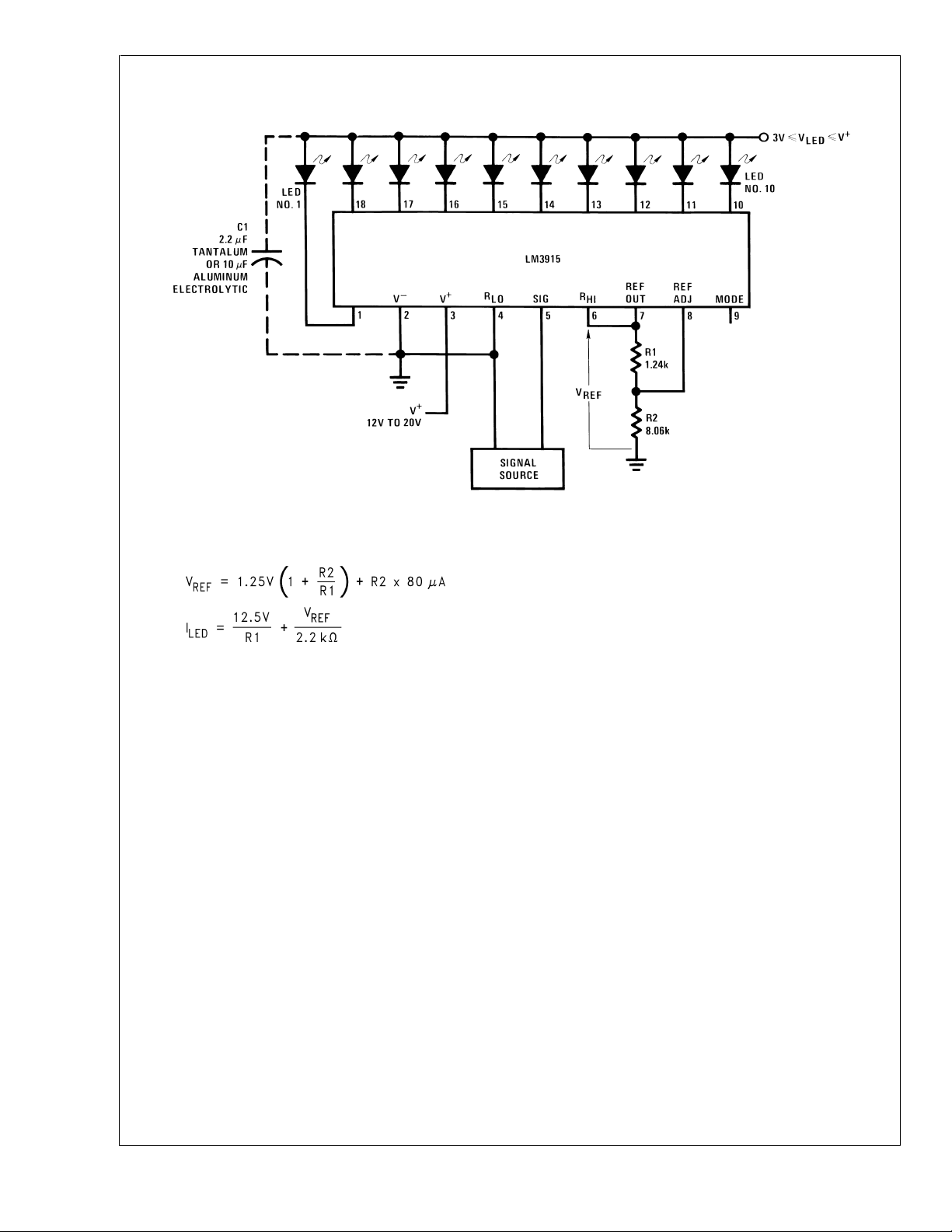
Typical Applications
LM3915
Notes: Capacitor C1 is required if leads to the LED supply are 6" or longer.
Circuit as shown is wired for dot mode. For bar mode, connect pin 9 to pin 3. V
dissipation.
0V to 10V Log Display
must be kept below 7V or dropping resistor should be used to limit IC power
LED
DS005104-1
www.national.com 2
Page 3
LM3915
Absolute Maximum Ratings (Note 1)
If Military/Aerospace specified devices are required,
please contact the National Semiconductor Sales Office/
Distributors for availability and specifications.
Power Dissipation (Note 6)
Molded DIP(N) 1365 mW
Supply Voltage 25V
Voltage on Output Drivers 25V
Input Signal Overvoltage (Note 4)
±
Divider Voltage −100 mV to V
Reference Load Current 10 mA
Storage Temperature Range −55˚C to +150˚C
Lead Temperature
(Soldering, 10 sec.) 260˚C
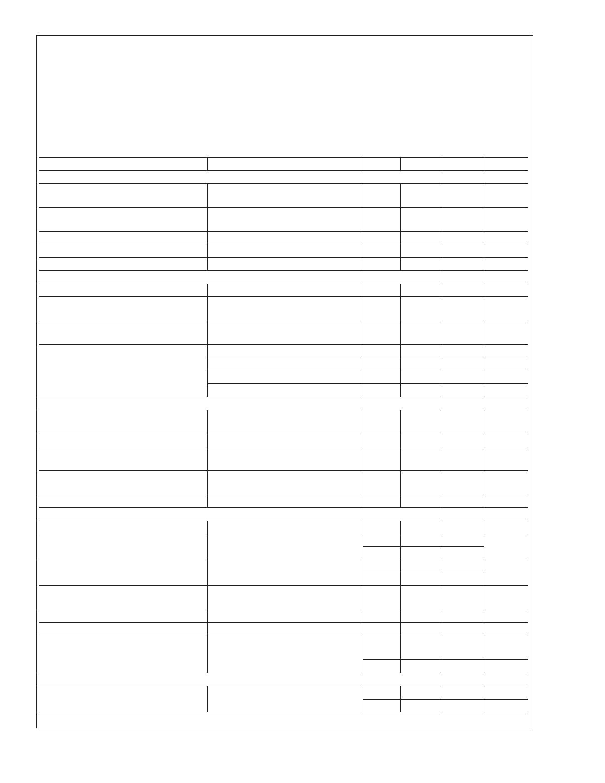
Electrical Characteristics (Notes 2, 4)
Parameter Conditions (Note 2) Min Typ Max Units
COMPARATOR
Offset Voltage, Buffer and First
Comparator
Offset Voltage, Buffer and Any Other
Comparator
Gain (∆I
/∆VIN)I
LED
Input Bias Current (at Pin 5) 0V ≤ V
Input Signal Overvoltage No Change in Display −35 35 V
VOLTAGE-DIVIDER
Divider Resistance Total, Pin 6 to 4 16 28 36 kΩ
Relative Accuracy (Input Change
Between Any Two Threshold Points)
Absolute Accuracy at Each Threshold
Point
VOLTAGE REFERENCE
Output Voltage 0.1 mA ≤ I
Line Regulation 3V ≤ V
Load Regulation 0.1 mA ≤ I
Output Voltage Change with
Temperature
Adjust Pin Current 75 120 µA
OUTPUT DRIVERS
LED Current V
LED Current Difference (Between
Largest and Smallest LED Currents)
LED Current Regulation 2V ≤ V
Dropout Voltage I
Saturation Voltage I
Output Leakage, Each Collector (Bar Mode) (Note 5) 0.1 10 µA
Output Leakage
Pins 10–18
Pin 1 60 150 450 µA
SUPPLY CURRENT
Standby Supply Current
(All Outputs Off)
0V ≤ V
=1mA
I
LED
0V ≤ V
=1mA
I
LED
L(REF)
(Note 3)
RLO=VRHI
RLO=VRHI
= 2 mA, I
≤ (V+− 1.5V) 25 100 nA
IN
≤ 12V,
≤ 12V,
= 10 mA 3 8 mA/mV
LED
310mV
315mV
2.0 3.0 4.0 dB
(Note 3)
V
= −3, −6 dB −0.5 +0.5 dB
IN
V
= −9 dB −0.5 +0.65 dB
IN
V
= −12, −15, −18 dB −0.5 +1.0 dB
IN
V
= −21, −24, −27 dB −0.5 +1.5 dB
IH
≤ 4 mA,
+
=V
V
+
=V
V
0˚C ≤ T
+
=V
V
+
=V
V
LED
V
LED
=20mA
I
LED
LED(ON)
∆I
LED
= 2.0 mA, I
LED
L(REF)
=5V
LED
+
≤ 18V 0.01 0.03 %/V
≤ 4 mA,
L(REF)
=5V
LED
≤ +70˚C, I
A
=5V
LED
= 5V, I
LED
= 5V, I
LED
= 5V, I
LED
≤ 17V, I
LED
= 20 mA,@V
=2mA
20 mA
= 1 mA,
L(REF)
= 1 mA 7 10 13 mA
L(REF)
=2mA
LED
= 5V,
LED
=2mA
= 0.4 mA 0.15 0.4 V
L(REF)
1.2 1.28 1.34 V
0.4 2 %
1%
0.12 0.4
1.2 3
0.1 0.25
13
1.5 V
(Dot Mode) (Note 5)
0.1 10 µA
+
V
= +5V, I
+
= +20V, I
V
L(REF)
L(REF)
= 0.2 mA
= 1.0 mA
2.4 4.2 mA
6.1 9.2 mA
mA
mA
35V
+
www.national.com3
Page 4
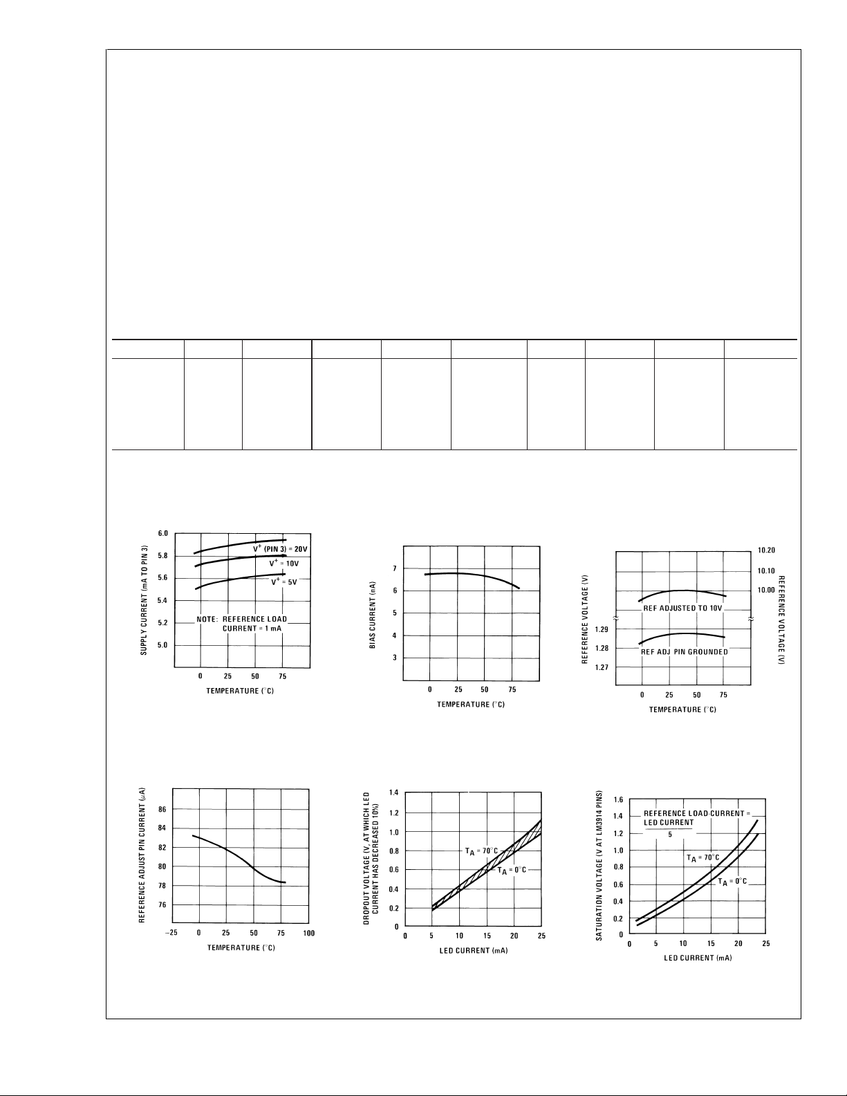
Electrical Characteristics (Notes 2, 4) (Continued)
Note 1: Absolute Maximum Ratings indicate limits beyond which damage to the device may occur. Operating Ratings indicate conditions for which the device is
LM3915
functional, but do not guarantee specific performance limits. Electrical Characteristics state DC and AC electrical specifications under particular test conditions which
guarantee specific performance limits. This assumes that the device is within the Operating Ratings. Specifications are not guaranteed for parameters where no limit
is given, however, the typical value is a good indication of device performance.
Note 2: Unless otherwise stated, all specifications apply with the following conditions:
3V
≤ V+≤ 20 V
DC
3V
≤ V
LED
RHI
≤ V
≤ 12 V
DC
−0.015V ≤ V
Note 3: Accuracyis measured referred to 0 dB = + 10.000 V
comparator offset voltage may add significant error. See table for threshold voltages.
Note 4: Pin 5 input current must be limited to
Note 5: Bar mode results when pin 9 is within 20 mV of V
disabled if pin 9 is pulled 0.9V or more below V
Note 6: Themaximum junction temperature of the LM3915 is 100˚C. Devices must be derated for operation at elevated temperatures. Junction to ambient thermal
resistance is 55˚C/W for the molded DIP (N package).
DC
+
−0.015V ≤ V
V
REF,VRHI,VRLO
0V ≤ VIN≤ V+− 1.5V
DC
≤ 12 V
RLO
≤ (V+− 1.5V) For higher power dissipations, pulse testing is used.
±
3 mA. The addition of a 39k resistor in series with pin 5 allows±100V signals without damage.
.
LED
TA= 25˚C, I
DC
at pin 5, with + 10.000 VDCat pin 6, and 0.000 VDCat pin 4. At lower full scale voltages, buffer and
DC
+
. Dot mode results when pin 9 is pulled at least 200 mV below V+. LED#10 (pin 10 output current) is
= 0.2 mA, pin 9 connected to pin 3 (bar mode).
L(REF)
Threshold Voltage (Note 3)
Output dB Min Typ Max Output dB Min Typ Max
1 −27 0.422 0.447 0.531 6 −12 2.372 2.512 2.819
2 −24 0.596 0.631 0.750 7 −9 3.350 3.548 3.825
3 −21 0.841 0.891 1.059 8 −6 4.732 5.012 5.309
4 −18 1.189 1.259 1.413 9 −3 6.683 7.079 7.498
5 −15 1.679 1.778 1.995 10 0 9.985 10 10.015
Typical Performance Characteristics
Supply Current vs Temperature
DS005104-34
Reference Adjust Pin
Current vs Temperature
Operating Input Bias Current vs
Temperature
LED Current-Regulation
Dropout
DS005104-35
Reference Voltage vs
Temperature
DS005104-36
LED Driver Saturation
Voltage
DS005104-37
www.national.com 4
DS005104-38
DS005104-39
Page 5

Typical Performance Characteristics (Continued)
LM3915
Input Current Beyond
Signal Range (Pin 5)
Total Divider Resistance
vs Temperature
DS005104-40
LED Current vs
Reference Loading
Common-Mode Limits
DS005104-41
LED Driver Current
Regulation
DS005104-42
Output Characteristics
DS005104-43
DS005104-44
DS005104-45
www.national.com5
Page 6
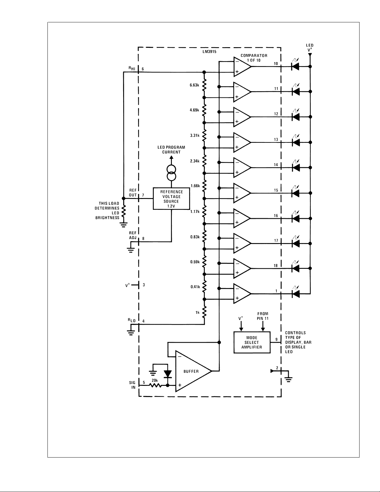
Block Diagram (Showing Simplest Application)
LM3915
www.national.com 6
DS005104-4
Page 7

LM3915
Functional Description
The simplified LM3915 block diagram is included to give the
general idea of the circuit’s operation. A high input impedance buffer operates with signals from ground to 12V, and is
protected against reverse and overvoltage signals. The signal is then applied to a series of 10 comparators; each of
which is biased to a different comparison level by the resistor
string.
In the example illustrated, the resistor string is connected to
the internal 1.25V reference voltage. In this case, for each
3 dB that the input signal increases, a comparator will switch
on another indicating LED. This resistor divider can be connected between any 2 voltages, providing that they are at
least 1.5V below V
INTERNAL VOLTAGE REFERENCE
The reference is designed to be adjustable and develops a
nominal 1.25V between the REF OUT (pin 7) and REF ADJ
(pin 8) terminals. The reference voltage is impressed across
program resistor R1 and, since the voltage is constant, a
constant current I
R2 giving an output voltage of:
Since the 120 µA current (max) from the adjust terminal
represents an error term, the reference was designed to
minimize changes of this current with V
For correct operation, reference load current should be between 80 µA and 5 mA. Load capacitance should be less
than 0.05 µF.
CURRENT PROGRAMMING
A feature not completely illustrated by the block diagram is
the LED brightness control. The current drawn out of the
reference voltage pin (pin 7) determines LED current. Approximately 10 times this current will be drawn through each
lighted LED, and this current will be relatively constant despite supply voltage and temperature changes. Current
drawn by the internal 10-resistor divider, as well as by the
external current and voltage-setting divider should be included in calculating LED drive current. The ability to modulate LED brightness with time, or in proportion to input voltage and other signals can lead to a number of novel displays
or ways of indicating input overvoltages, alarms, etc.
The LM3915 outputs are current-limited NPN transistors as
shown below. An internal feedback loop regulates the transistor drive. Output current is held at about 10 times the
reference load current, independent of output voltage and
processing variables, as long as the transistor is not saturated.
+
and no lower than V−.
then flows through the output set resistor
1
DS005104-5
+
and load changes.
LM3915 Output Circuit
DS005104-6
Outputs may be run in saturation with no adverse effects,
making it possible to directly drive logic. The effective saturation resistance of the output transistors, equal to R
plus
E
the transistors’ collector resistance, is about 50Ω. It’s also
possible to drive LEDs from rectified AC with no filtering. To
avoid oscillations, the LED supply should be bypassed with a
2.2 µF tantalum or 10 µF aluminum electrolytic capacitor.
MODE PIN USE
Pin 9, the Mode Select input, permits chaining of multiple
LM3915s, and controls bar or dot mode operation. The
following tabulation shows the basic ways of using this input.
Other more complex uses will be illustrated in the applications.
Bar Graph Display: Wire Mode Select (pin 9)
+
3(V
pin).
directly
to pin
Dot Display, Single LM3915 Driver: Leave the Mode Select
pin open circuit.
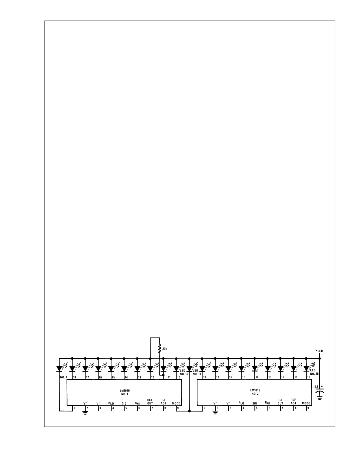
Dot Display, 20 or More LEDs: Connect pin 9 of the
first
driver in the series (i.e., the one with the lowest input voltage
comparison points) to pin 1 of the next higher LM3915 driver.
Continue connecting pin 9 of lower input drivers to pin 1 of
higher input drivers for 30 or more LED displays. The last
LM3915 driver in the chain will have pin 9 left open. All
previous drivers should have a 20k resistor in parallel with
#
LED
9 (pin 11 to V
LED
).
Mode Pin Functional Description
This pin actually performs two functions. Refer to the simplified block diagram below.
Block Diagram of Mode Pin Function
DS005104-7
*
High for bar
www.national.com7
Page 8
Mode Pin Functional Description
(Continued)
LM3915
DOT OR BAR MODE SELECTION
The voltage at pin 9 is sensed by comparator C1, nominally
referenced to (V
pin 9 is above this level; otherwise it’s in dot mode. The
comparator is designed so that pin 9 can be left open circuit
for dot mode.
Taking into account comparator gain and variation in the
100 mV reference level, pin 9 should be no more than 20 mV
below V
+
open circuit) for dot mode. In most applications, pin 9 is
either open (dot mode) or tied to V
pin 9 should be connected directly to pin 3. Large currents
drawn from the power supply (LED current, for example)
should not share this path so that large IR drops are avoided.
DOT MODE CARRY
In order for the display to make sense when multiple
LM3915s are cascaded in dot mode, special circuitry has
been included to shut off LED
#
LED
1 of the second device comes on. The connection for
cascading in dot mode has already been described and is
depicted below.
As long as the input signal voltage is below the threshold of
the second LM3915, LED
sees effectively an open circuit so the chip is in dot mode.As
soon as the input voltage reaches the threshold of LED
pin 9 of LM3915
below V
referenced 600 mV below V
low, which shuts off output transistor Q2, extinguishing LED
#
10.
V
is sensed via the 20k resistor connected to pin 11. The
LED
very small current (less than 100 µA) that is diverted from
#
LED
9 does not noticeably affect its intensity.
An auxiliary current source at pin 1 keeps at least 100 µA
flowing through LED
enough to extinguish the LED. This ensures that pin 9 of
LM3915
any
higher LED is illuminated. While 100 µA does not normally produce significant LED illumination, it may be noticeable when using high-efficiency LEDs in a dark environment.
If this is bothersome, the simple cure is to shunt LED
with a 10k resistor. The 1V IR drop is more than the 900 mV
worst case required to hold off LED
that LED
+
− 100 mV). The chip is in bar mode when
for bar mode and more than 200 mV below V+(or
+
(bar mode). In bar mode,
#
10 of the first device when
#
11is off. Pin 9 of LM3915#1 thus
#
1 is pulled an LED drop (1.5V or more)
. This condition is sensed by comparator C2,
LED
#
11 even if the input voltage rises high
#
1 is held low enough to force LED#10 off when
#
11 does not conduct significantly.
. This forces the output of C2
LED
#
10 yet small enough
OTHER DEVICE CHARACTERISTICS
The LM3915 is relatively low-powered itself, and since any
number of LEDs can be powered from about 3V, it is a very
efficient display driver. Typical standby supply current (all
LEDs OFF) is 1.6 mA. However, any reference loading adds
4 times that current drain to the V
+
(pin 3) supply input. For
example, an LM3916 witha1mAreference pin load (1.3k)
would supply almost 10 mA to every LED while drawing only
10 mA from its V
+
pin supply. At full-scale, the IC is typically
drawing less than 10% of the current supplied to the display.
The display driver does not have built-in hysteresis so that
the display does not jump instantly from one LED to the next.
Under rapidly changing signal conditions, this cuts down
high frequency noise and often an annoying flicker.An “overlap” is built in so that at no time are all segments completely
off in the dot mode. Generally 1 LED fades in while the other
fades out over a mV or more of range. The change may be
much more rapid between LED
#
1ofa
second
device “chained” to the first.
#
10 of one device and LED
Application Hints
The most difficult problem occurs when large LED currents
are being drawn, especially in bar graph mode. These currents flowing out of the ground pin cause voltage drops in
external wiring, and thus errors and oscillations. Bringing the
return wires from signal sources, reference ground and bottom of the resistor string to a single point very near pin 2 is
#
11,
#
11
the best solution.
Long wires from V
to LED anode common can cause
LED
oscillations. Depending on the severity of the problem
0.05 µF to 2.2 µF decoupling capacitors from LED anode
common to pin 2 will damp the circuit. If LED anode line
wiring is inaccessible, often similar decoupling from pin 1 to
pin 2 will be sufficient.
If LED turn ON seems slow (bar mode) or several LEDs light
(dot mode), oscillation or excessive noise is usually the
problem. In cases where proper wiring and bypassing fail to
stop oscillations, V
+
voltage at pin 3 is usually below suggested limits. Expanded scale meter applications may have
one or both ends of the internal voltage divider terminated at
relatively high value resistors. These high-impedance ends
should be bypassed to pin 2 with at least a 0.001 µF capacitor, or up to 0.1 µF in noisy environments.
Cascading LM3915s in Dot Mode
www.national.com 8
DS005104-8
Page 9
Application Hints (Continued)
Power dissipation, especially in bar mode should be given
consideration. For example, with a 5V supply and all LEDs
programmed to 20 mA the driver will dissipate over 600 mW.
In this case a 7.5Ω resistor in series with the LED supply will
cut device heating in half. The negative end of the resistor
should be bypassed with a 2.2 µF solid tantalum capacitor to
pin 2.
TIPS ON RECTIFIER CIRCUITS
The simplest way to display an AC signal using the LM3915
is to apply it right to pin 5 unrectified. Since the LED illuminated represents the instantaneous value of the AC waveform, one can readily discern both peak and average values
of audio signals in this manner. The LM3915 will respond to
positive half-cycles only but will not be damaged by signals
±
up to
35V (or up to±100V if a 39k resistor is in series with
the input). It’s recommended to use dot mode and to run the
LEDs at 30 mA for high enough average intensity.
True average or peak detection requires rectification. If an
LM3915 is set up with 10V full scale across its voltage
divider, the turn-on point for the first LED is only 450 mV. A
simple silicon diode rectifier won’t work well at the low end
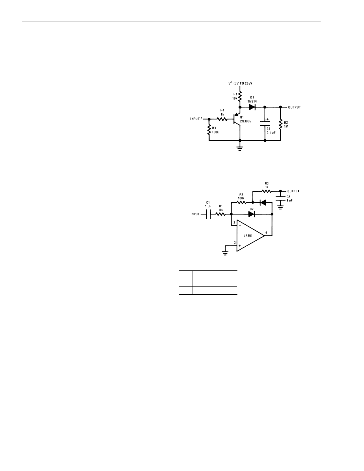
due to the 600 mV diode threshold. The half-wave peak
detector in
the diode. Now, the transistor’s base-emitter voltage cancels
out the diode offset, within about 100 mV. This approach is
usually satisfactory when a single LM3915 is used for a 30
dB display.
Display circuits using two or more LM3915s for a dynamic
range of 60 dB or greater require more accurate detection. In
the precision half-wave rectifier of
diode offset is reduced by a factor equal to the open-loop
gain of the op amp. Filter capacitor C2 charges through R3
and discharges through R2 and R3, so that appropriate
selection of these values results in either a peak or an
average detector. The circuit has a gain equal to R2/R1.
It’s best to capacitively couple the input. Audio sources
frequently have a small DC offset that can cause significant
error at the low end of the log display. Op amps that slew
quickly, such as the LF351, LF353, or LF356, are needed to
faithfully respond to sudden transients. It may be necessary
to trim out the op amp DC offset voltage to accurately cover
a 60 dB range. Best results are obtained if the circuit is
adjusted for the correct output when a low-level AC signal
(10 mV to 20 mV) is applied, rather than adjusting for zero
output with zero input.
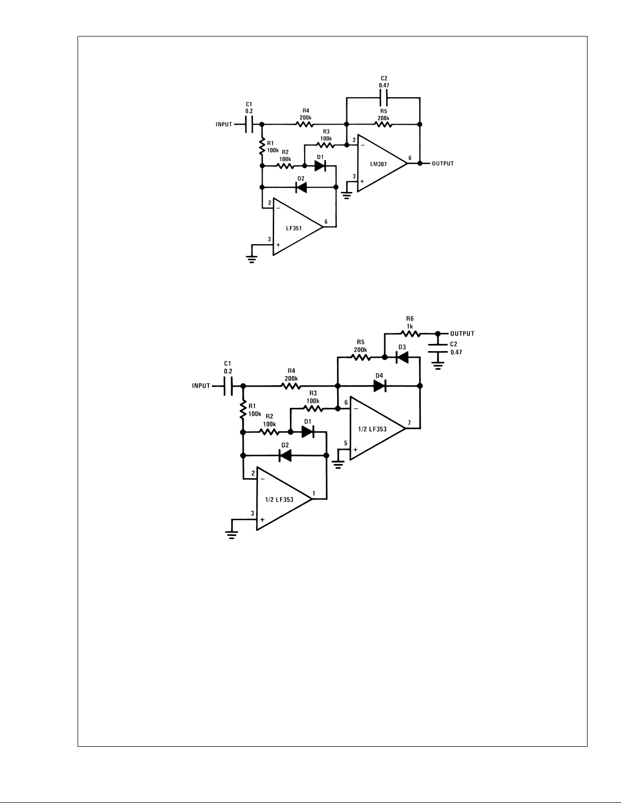
For precision full-wave averaging use the circuit in
Using 1% resistors for R1 through R4, gain for positive and
Figure 1
uses a PNP emitter-follower in front of
Figure 2
the effective
Figure 3
LM3915
negative signal differs by only 0.5 dB worst case. Substituting 5% resistors increases this to 2 dB worst case. (A 2 dB
gain difference means that the display may have a
error when the input is a nonsymmetrical transient). The
averaging time constant is R5–C2. A simple modification
results in the precision full-wave detector of
Figure 4
the filter capacitor is not buffered, this circuit can drive only
high impedance loads such as the input of an LM3915.
*
DC Couple
FIGURE 1. Half-Wave Peak Detector
D1, D2: 1N914 or 1N4148
Average Peak
R2 1k 100k
R3 100k 1k
R1 = R2 for AV=1
R1 = R2/R10 for A
C1 = 10/R1
V
=10
FIGURE 2. Precision Half-Wave Rectifier
.
. Since
DS005104-9
DS005104-10
±
1dB
www.national.com9
Page 10
Application Hints (Continued)
LM3915
D1, D2: 1N914 or 1N4148
DS005104-11
FIGURE 3. Precision Full-Wave Average Detector
D1, D2, D3, D4: 1N914 or 1N4148
FIGURE 4. Precision Full-Wave Peak Detector
CASCADING THE LM3915
To display signals of 60 dB or 90 dB dynamic range, multiple
LM3915s can be easily cascaded. Alternatively,it is possible
to cascade an LM3915 with LM3914s for a log/linear display
or with an LM3916 to get an extended range VU meter.
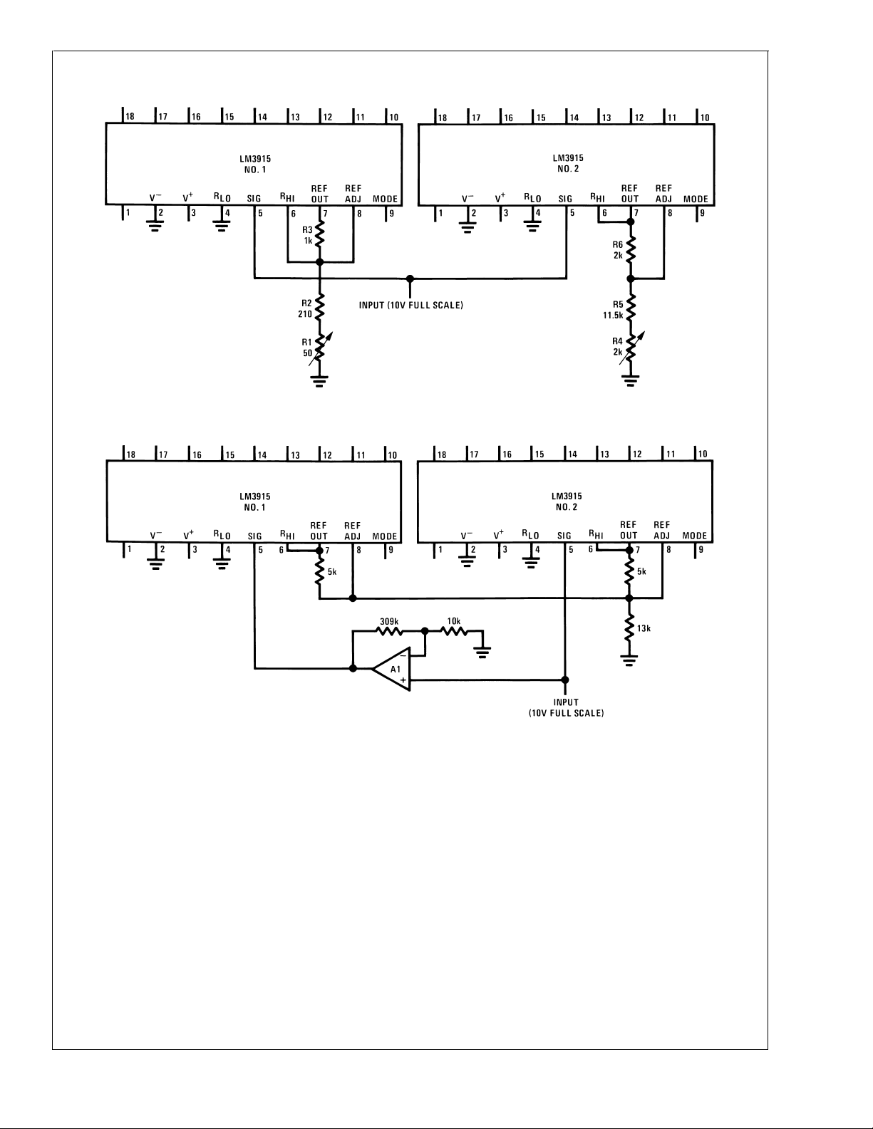
A simple, low cost approach to cascading two LM3915s is to
set the reference voltages of the two chips 30 dB apart as in
Figure 5
voltage of LM3915
. Potentiometer R1 is used to adjust the full scale
#
1 to 316 mV nominally while the second
IC’s reference is set at 10V by R4. The drawback of this
method is that the threshold of LED
#
1 is only 14 mV and,
since the LM3915 can have an offset voltage as high as
10 mV, large errors can occur. This technique is not recommended for 60 dB displays requiring good accuracy at the
first few display thresholds.
www.national.com 10
DS005104-12
Abetter approach shown in
Figure 6
is to keep the reference
at 10V for both LM3915s and amplify the input signal to the
lower LM3915 by 30 dB. Since two 1% resistors can set the
amplifier gain within
±
0.2 dB, a gain trim is unnecessary.
However, an op amp offset voltage of 5 mV will shift the first
LED threshold as much as 4 dB, so that an offset trim may
be required. Note that a single adjustment can null out offset
in both the precision rectifier and the 30 dB gain stage.
Alternatively, instead of amplifying, input signals of sufficient
amplitude can be fed directly to the lower LM3915 and
attenuated
by 30 dB to drive the second LM3915.
Page 11
Application Hints (Continued)
FIGURE 5. Low Cost Circuit for 60 dB Display
LM3915
DS005104-13
FIGURE 6. Improved Circuit for 60 dB Display
To extend this approach to get a 90 dB display, another
30 dB of amplification must be placed in the signal path
ahead of the lowest LM3915. Extreme care is required as the
lowest LM3915 displays input signals down to 0.5 mV! Several offset nulls may be required. High currents should not
share the same path as the low level signal. Also power line
wiring should be kept away from signal lines.
TIPS ON REFERENCE VOLTAGE
AND LED CURRENT PROGRAMMING
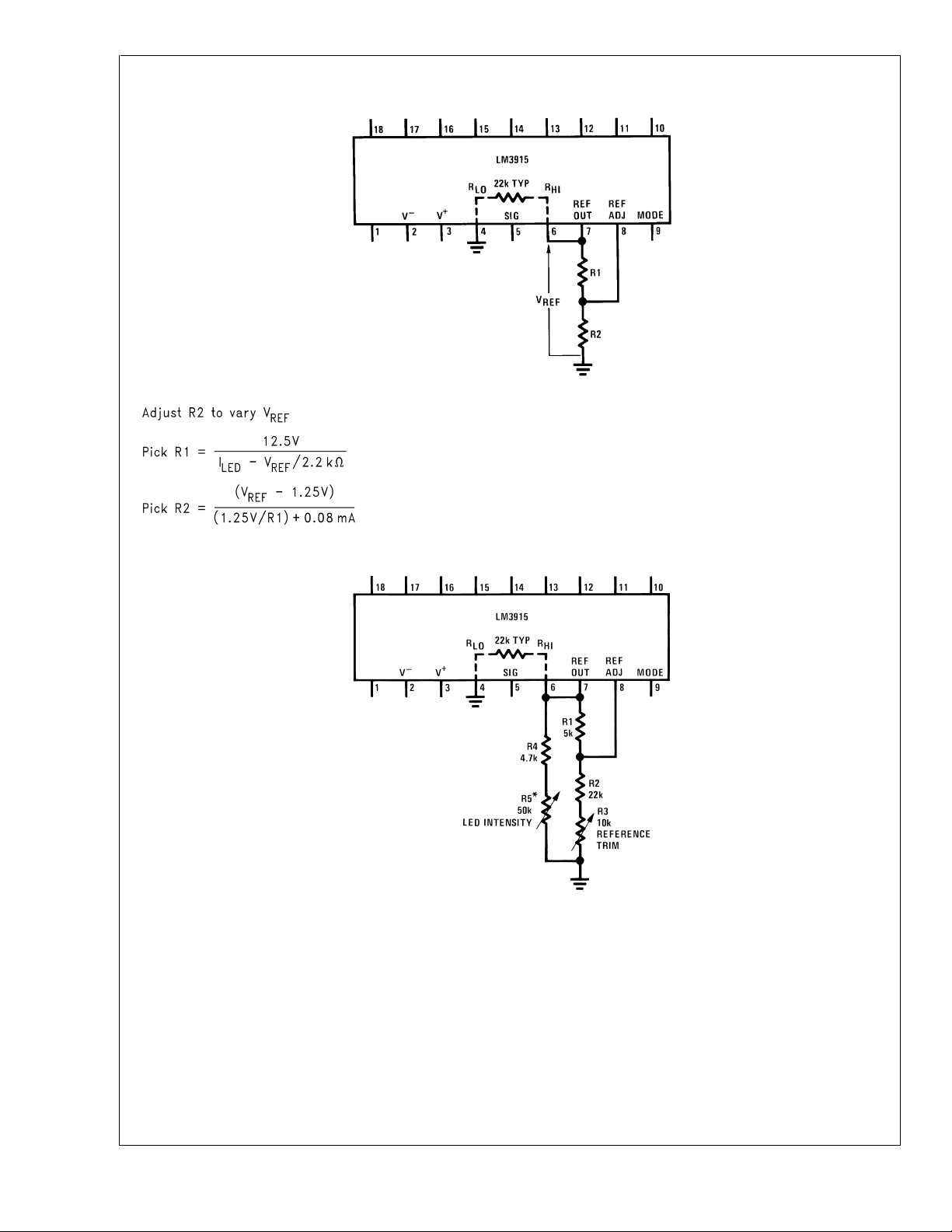
SINGLE LM3915
The equations in
Figure 7
illustrate how to choose resistor
values to set reference voltage for the simple case where no
LED intensity adjustment is required. ALED current of 10 mA
to 20 mA generally produces adequate illumination. Having
10V full-scale across the internal voltage divider gives best
accuracy by keeping signal level high relative to the offset
voltage of the internal comparators. However, this causes
DS005104-14
450 µA to flow from pin 7 into the divider which means that
the LED current will be at least 5 mA. R1 will typically be
between 1 kΩ and2kΩ. To trim the reference voltage, vary
R2.
The circuit in
Figure 8
shows how to add a LED intensity
control which can vary LED current from 9 mAto 28 mA. The
reference adjustment has some effect on LED intensity but
the reverse is not true.
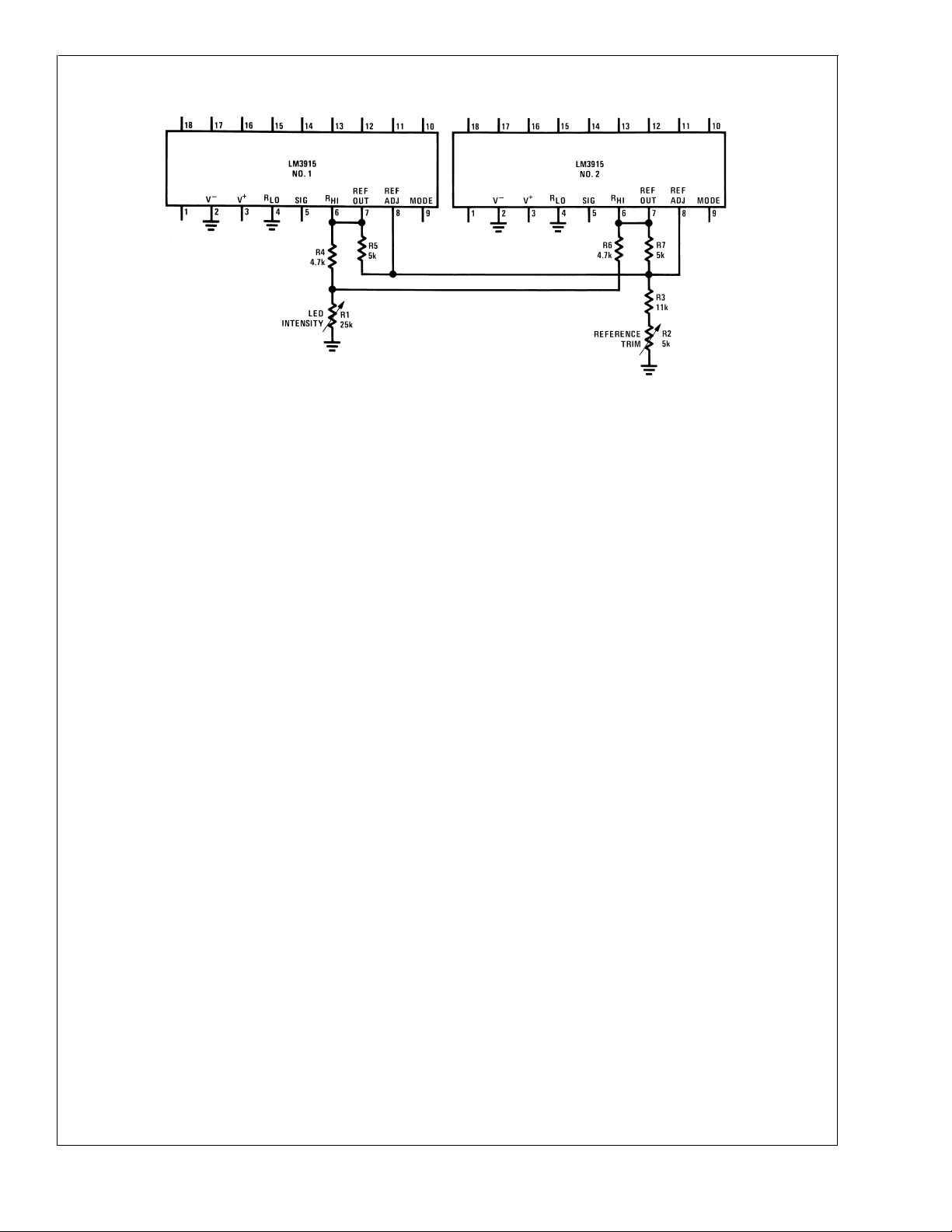
MULTIPLE LM3915s
Figure 9
shows how to obtain a common reference trim and
intensity control for two LM3915s. The two ICs may be
connected in cascade for a 60 dB display or may be handling
separate channels for stereo. This technique can be extended for larger numbers of LM3915s by varying the values
of R1, R2 and R3 in inverse proportion to the number of
devices tied in. The ICs’ internal references track within
100 mV so that worst case error from chip to chip is only
0.1 dB for V
REF
= 10V.
www.national.com11
Page 12
Application Hints (Continued)
LM3915
DS005104-15
*
9mA<I
LED
<
28 mA@V
REF
FIGURE 7. Design Equations for Fixed LED Intensity
DS005104-16
= 10V
FIGURE 8. Varying LED Intensity
www.national.com 12
Page 13
Application Hints (Continued)
FIGURE 9. Independent Adjustment of Reference Voltage and LED Intensity for Multiple LM3915s
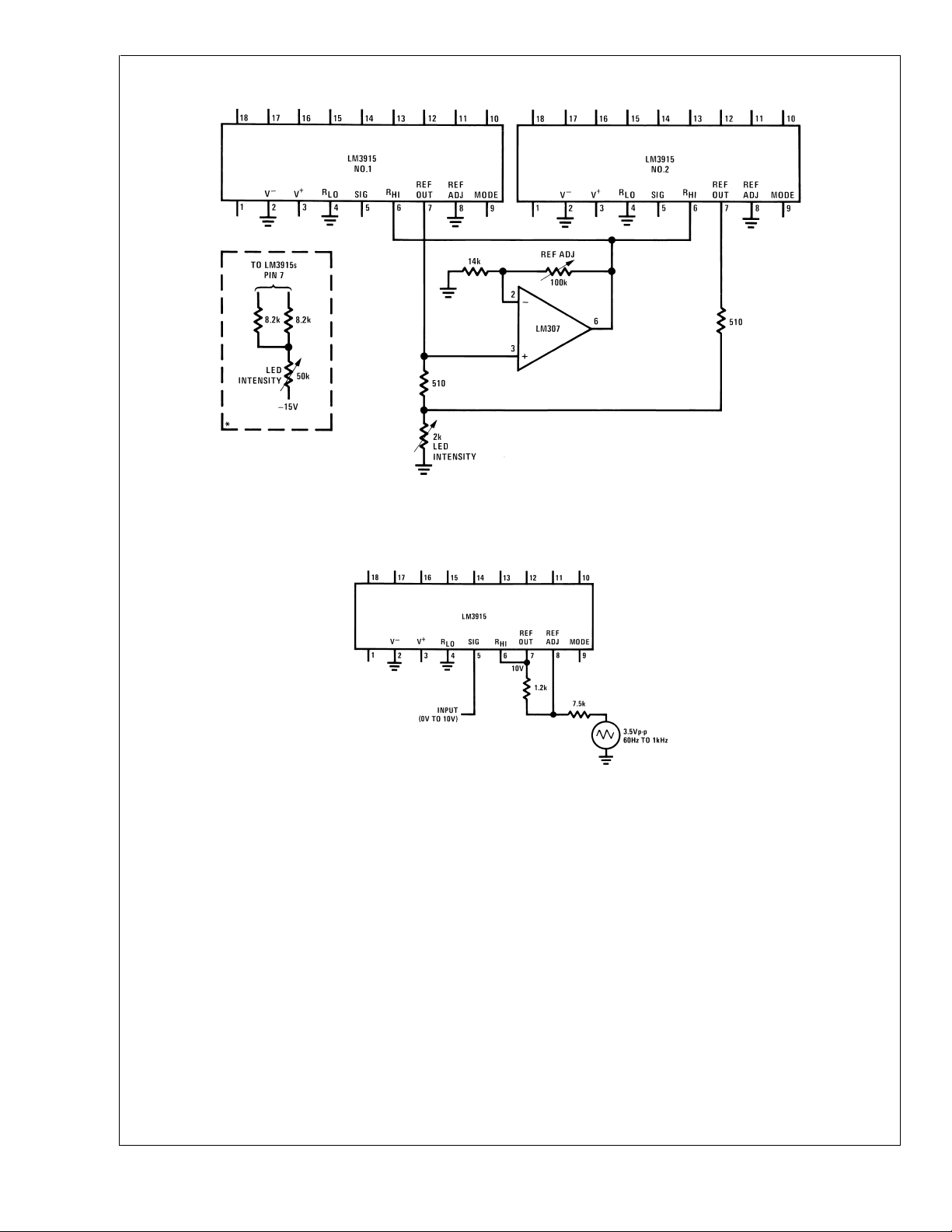
The scheme in
LED intensity must be adjusted independently over a wide
range. The R
with no effect on LED current. Since the internal divider here
does not load down the reference, minimum LED current is
much lower. At the minimum recommended reference load
of 80 µA, LED current is about 0.8 mA. The resistor values
shown give a LED current range from 1.5 mA to 20 mA.
At the low end of the intensity adjustment, the voltage drop
across the 510Ω current-sharing resistors is so small that
chip to chip variation in reference voltage may yield a visible
variation in LED intensity. The optional approach shown of
connecting the bottom end of the intensity control pot to a
negative supply overcomes this problem by allowing a larger
voltage drop across the (larger) current-sharing resistors.
Figure 10
voltage can be adjusted from 1.2V to 10V
HI
is useful when the reference and
DS005104-17
Other Applications
For increased resolution, it’s possible to obtain a display with
a smooth transition between LEDs. This is accomplished by
varying the reference level at pin 6 by 3 dBp-p as shown in
Figure 11
wave from 60 Hz to 1 kHz. The display can be run in either
dot or bar mode.
When an exponentially decaying RC discharge waveform is
applied to pin 5, the LM3915’s outputs will switch at equal
intervals. This makes a simple timer or sequencer. Each time
interval is equal to RC/3. The output may be used to drive
logic, opto-couplers, relays or PNP transistors, for example.
. The signal can be a triangle, sawtooth or sine
LM3915
www.national.com13
Page 14
Typical Applications
LM3915
*
Optional circuit for improved intensity matching at low currents.
See text.
FIGURE 10. Wide-Range Adjustment of Reference Voltage and LED Intensity for Multiple LM3915s
DS005104-18
FIGURE 11. 0V to 10V Log Display with Smooth Transitions
www.national.com 14
DS005104-19
Page 15
Typical Applications (Continued)
LM3915
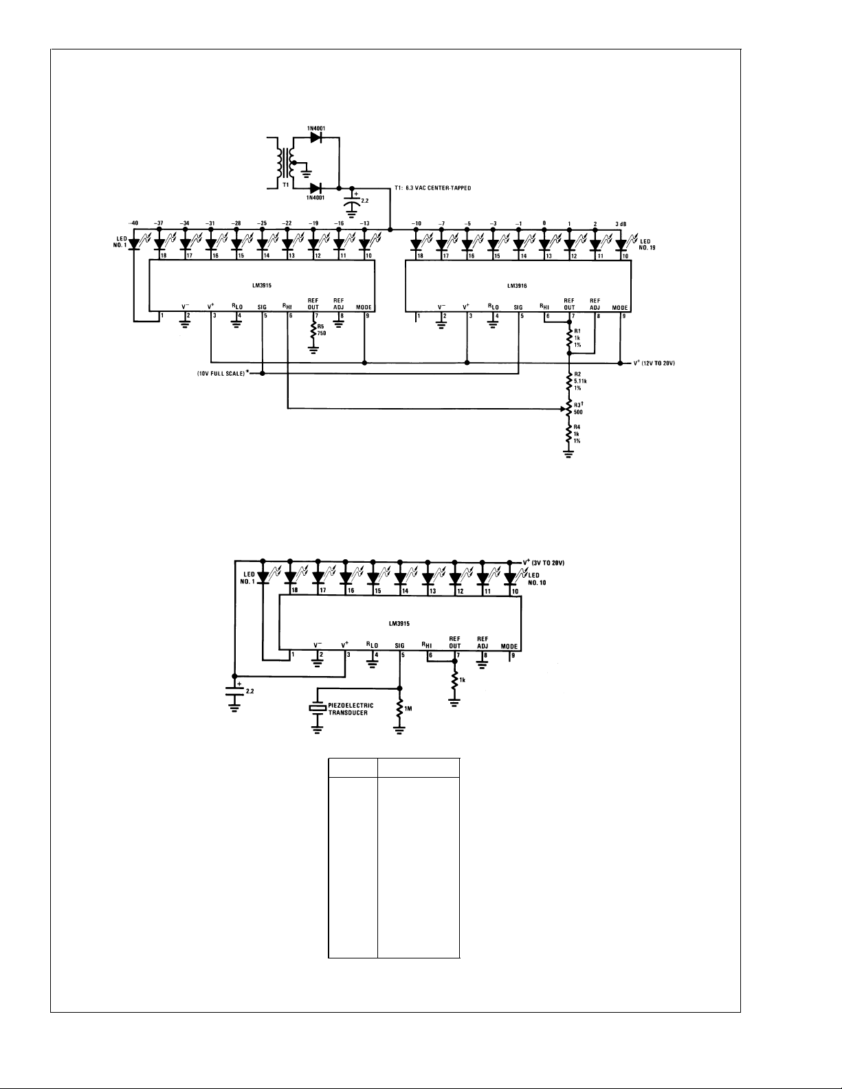
Extended Range VU Meter
This application shows that the LED supply requires minimal filtering.
*
See Application Hints for optional Peak or Average Detector.
†
Adjust R3 for 3 dB difference between LED#11 and LED#12.
DS005104-20
Vibration Meter
DS005104-21
LED Threshold
160mV
280mV
3 110 mV
4 160 mV
5 220 mV
6 320 mV
7 440 mV
8 630 mV
9 890 mV
10 1.25V
www.national.com15
Page 16
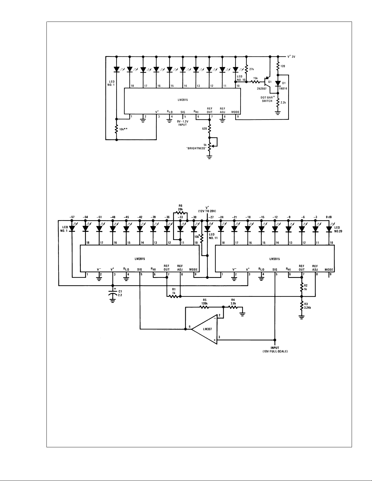
Typical Applications (Continued)
LM3915
Indicator and Alarm, Full-Scale Changes Display from Dot to Bar
*
The input to the dot bar switch may be taken from cathodes of other LEDs.
Display will change to bar as soon as the LED so selected begins to light.
**
Optional. Shunts 100 µA auxiliary sink current away from LED#1.
DS005104-22
60 dB Dot Mode Display
**
Optional. Shunts 100 µA auxiliary sink current away from LED#11.
www.national.com 16
DS005104-23
Page 17
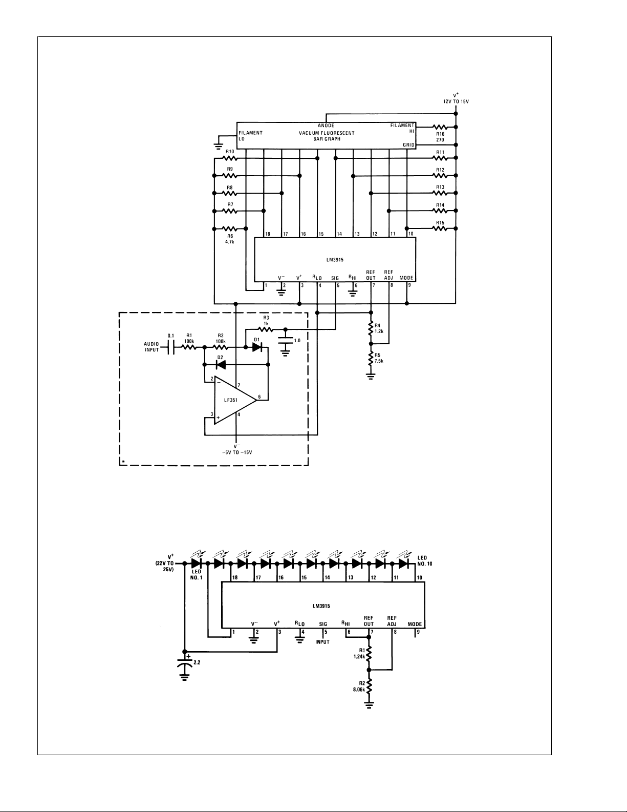
Typical Applications (Continued)
Driving Vacuum Fluorescent Display
LM3915
R7 thru R15: 10k±10%
D1, D2: 1N914 or 1N4148
*
Half-wave peak detector.
See Application Hints.
Supply current drain is only 15 mA with ten LEDs illuminated.
DS005104-24
Low Current Bar Mode Display
DS005104-25
www.national.com17
Page 18
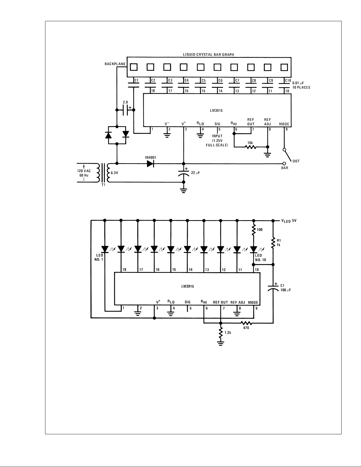
Typical Applications (Continued)
LM3915
Driving Liquid Crystal Display
DS005104-26
Bar Display with Alarm Flasher
DS005104-27
Full-scale causes the full bar display to flash. If the junction of R1 and C1 is connected to a different LED cathode, the display will flash when that LED lights,
and at any higher input signal.
www.national.com 18
Page 19
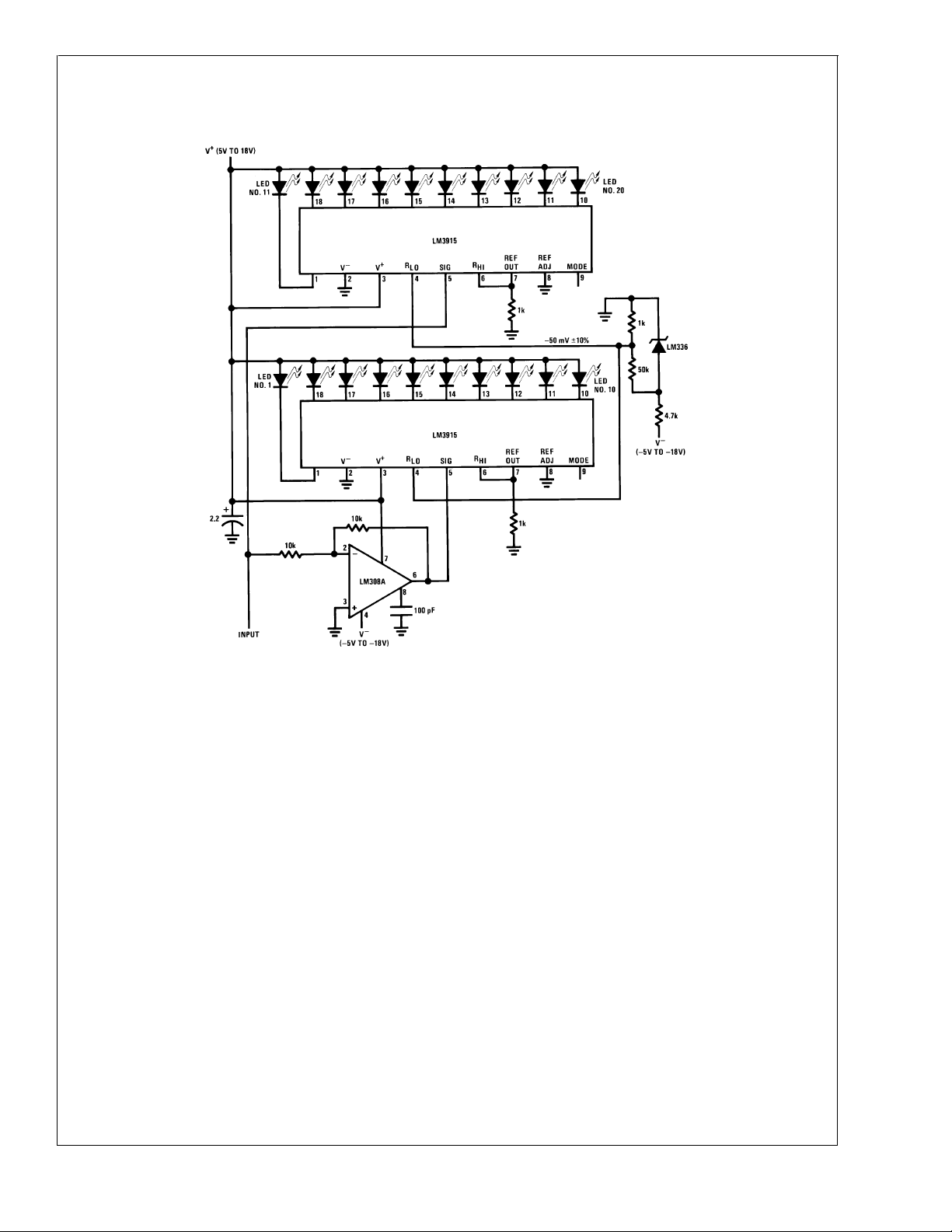
Typical Applications (Continued)
LM3915
Precision Null Meter
Logarithmic response allows coarse and fine adjustments without changing scale.
Resolution ranges from 10 mV at V
= 0 mV to 500 mV at VIN=±1.25V.
IN
DS005104-28
www.national.com19
Page 20
Typical Applications (Continued)
LM3915
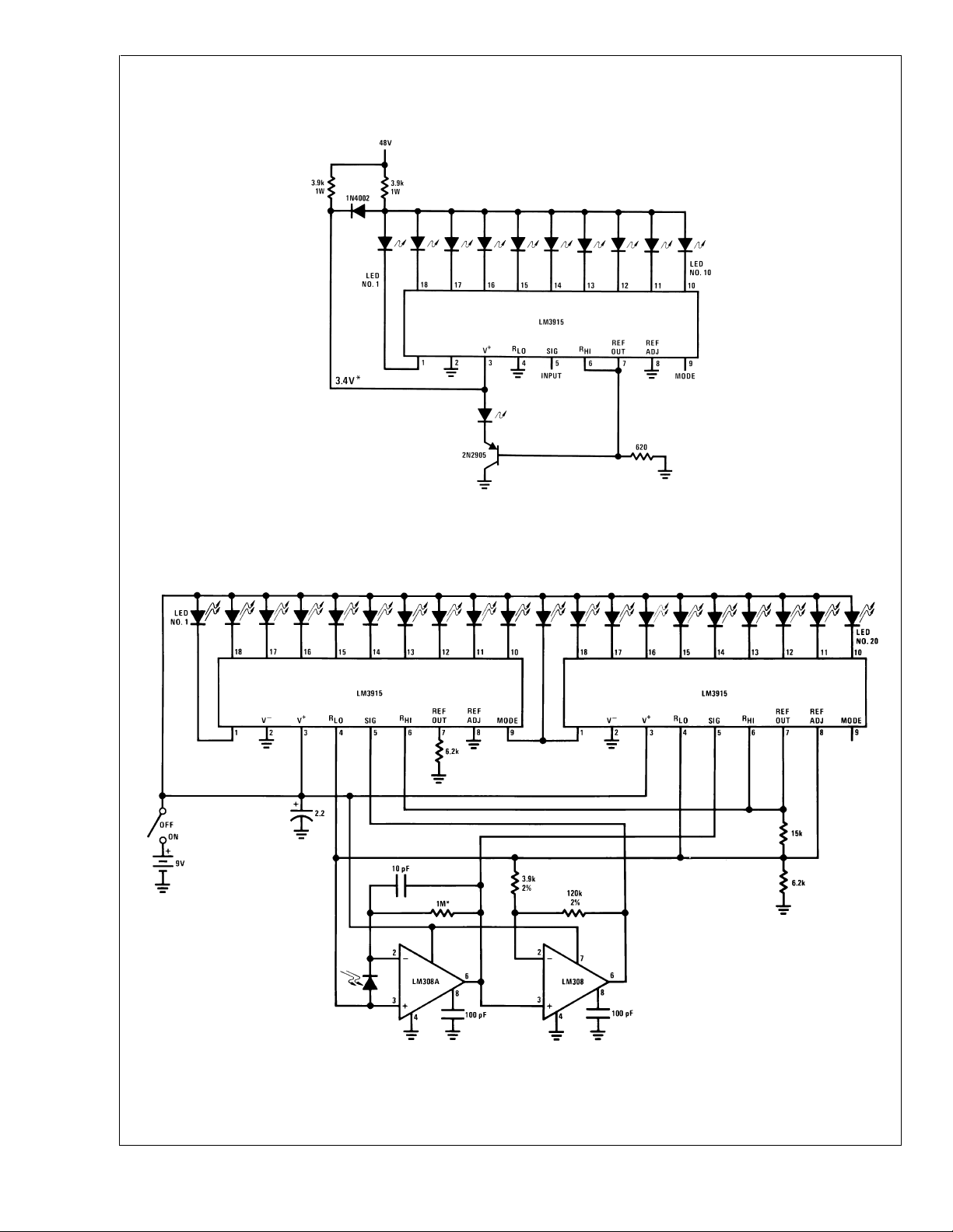
Operating with a High Voltage Supply (Dot Mode Only)
DS005104-29
The LED currents are approximately 10 mA, and the LM3915 outputs operate in saturation for minimum dissipation.
*
This point is partially regulated and decreases in voltage with temperature. Voltage requirements of the LM3915 also decrease with temperature.
Light Meter
*
Resistor value selects exposure
1/2 f/stop resolution
Ten f/stop range (1000:1)
Typical supply current is 8 mA.
www.national.com 20
DS005104-30
Page 21
Typical Applications (Continued)
LM3915
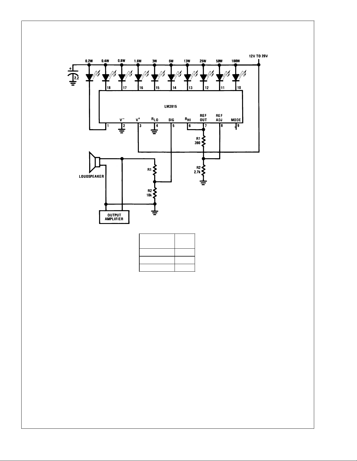
Audio Power Meter
Load
Impedance
R1
4Ω 10k
8Ω 18k
16Ω 30k
See Application Hints for optional Peak
or Average Detector
DS005104-31
www.national.com21
Page 22
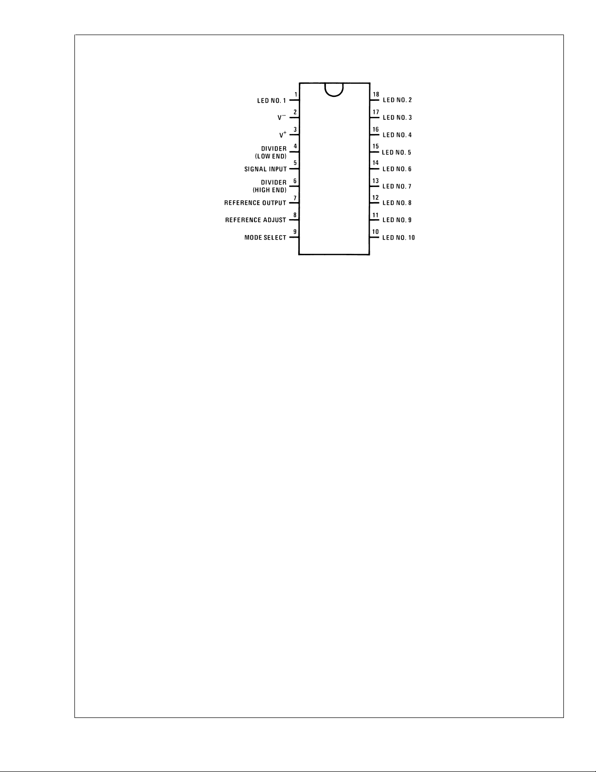
Connection Diagram
LM3915
*
Discontinued, Life Time Buy date 12/20/99
Definition of Terms
Absolute Accuracy: The difference between the observed
threshold voltage and the ideal threshold voltage for each
comparator. Specified and tested with 10V across the internal voltage divider so that resistor ratio matching error predominates over comparator offset voltage.
Adjust Pin Current: Current flowing out of the reference
adjust pin when the reference amplifier is in the linear region.
Comparator Gain: The ratio of the change in output current
(I
) to the change in input voltage (VIN) required to pro-
LED
duce it for a comparator in the linear region.
Dropout Voltage: The voltage measured at the current
source outputs required to make the output current fall by
10%.
Input Bias Current: Current flowing out of the signal input
when the input buffer is in the linear region.
LED Current Regulation: The change in output current over
the specified range of LED supply voltage (V
Dual-in-Line Package
Top View
Order Number LM3915N-1
See NS Package Number NA18A
Order Number LM3915N
*
See NS Package Number N18A
sured at the current source outputs. As the forward voltage
of an LED does not change significantly with a small change
in forward current, this is equivalent to changing the voltage
at the LED anodes by the same amount.
Line Regulation: The average change in reference output
voltage (V
+
(V
REF
).
Load Regulation: The change in reference output voltage
over the specified range of load current (I
Offset Voltage: The differential input voltage which must be
applied to each comparator to bias the output in the linear
region. Most significant error when the voltage across the
internal voltage divider is small. Specified and tested with pin
6 voltage (V
Relative Accuracy: The difference between any two adjacent threshold points. Specified and tested with 10V across
the internal voltage divider so that resistor ratio matching
error predominates over comparator offset voltage.
) as mea-
LED
DS005104-32
) over the specified range of supply voltage
).
L(REF)
) equal to pin 4 voltage (V
RHI
RLO
).
www.national.com 22
Page 23
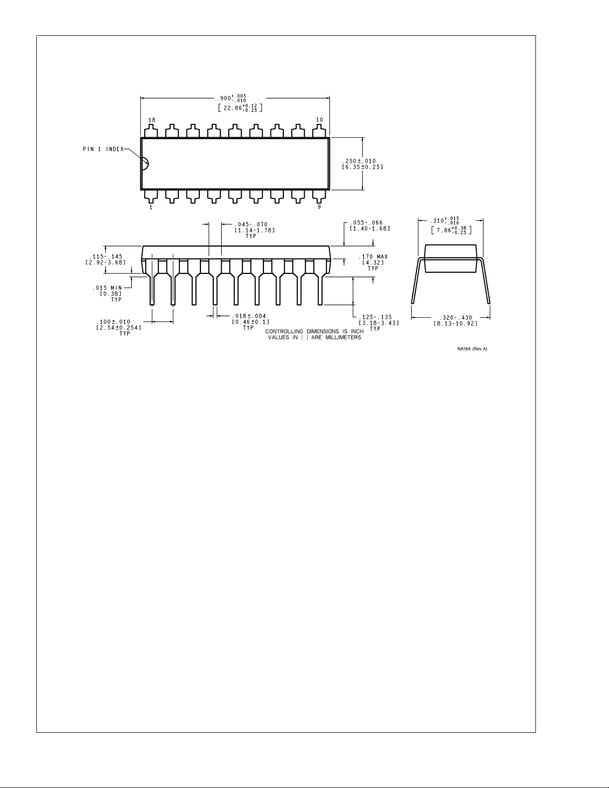
Physical Dimensions inches (millimeters) unless otherwise noted
LM3915
Note: Unless otherwise specified.
1. Standard Lead Finish:
200 microinches /5.08 micrometer minimum
lead/tin 37/63 or 15/85 on alloy 42 or equivalent or copper
2. Reference JEDEC registration MS-001, VariationAC, dated May 1993.
Molded Dual-In-Line Package (N)
Order Number LM3915N-1
NS Package Number NA18A
www.national.com23
Page 24
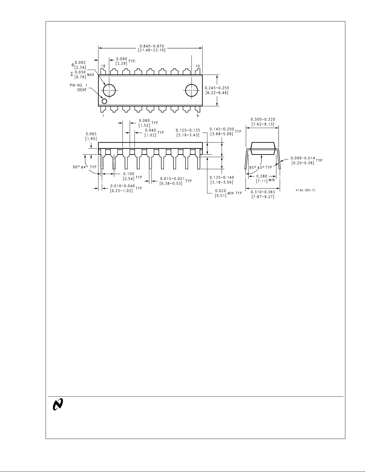
Physical Dimensions inches (millimeters) unless otherwise noted (Continued)
LM3915 Dot/Bar Display Driver
Molded Dual-In-Line Package (N)
Order Number LM3915N
*
NS Package Number N18A
*
Discontinued, Life Time Buy date 12/20/99
LIFE SUPPORT POLICY
NATIONAL’S PRODUCTS ARE NOT AUTHORIZED FOR USE AS CRITICAL COMPONENTS IN LIFE SUPPORT
DEVICES OR SYSTEMS WITHOUT THE EXPRESS WRITTEN APPROVAL OF THE PRESIDENT AND GENERAL
COUNSEL OF NATIONAL SEMICONDUCTOR CORPORATION. As used herein:
1. Life support devices or systems are devices or
systems which, (a) are intended for surgical implant
into the body, or (b) support or sustain life, and
whose failure to perform when properly used in
accordance with instructions for use provided in the
2. A critical component is any component of a life
support device or system whose failure to perform
can be reasonably expected to cause the failure of
the life support device or system, or to affect its
safety or effectiveness.
labeling, can be reasonably expected to result in a
significant injury to the user.
National Semiconductor
Corporation
Americas
Tel: 1-800-272-9959
Fax: 1-800-737-7018
Email: [email protected]
www.national.com
National does not assume any responsibility for use of any circuitry described, no circuit patent licenses are implied and National reserves the right at any time without notice to change said circuitry and specifications.
National Semiconductor
Europe
Fax: +49 (0) 180-530 85 86
Email: [email protected]
Deutsch Tel: +49 (0) 69 9508 6208
English Tel: +44 (0) 870 24 0 2171
Français Tel: +33 (0) 1 41 91 8790
National Semiconductor
Asia Pacific Customer
Response Group
Tel: 65-2544466
Fax: 65-2504466
Email: [email protected]
National Semiconductor
Japan Ltd.
Tel: 81-3-5639-7560
Fax: 81-3-5639-7507
 Loading...