

Page 1
LM389 Low Voltage Audio Power Amplifier
with NPN Transistor Array
Y
General Description
The LM389 is an array of three NPN transistors on the same
substrate with an audio power amplifier similar to the
LM386.
The amplifier inputs are ground referenced while the output
is automatically biased to one half the supply voltage. The
gain is internally set at 20 to minimize external parts, but the
addition of an external resistor and capacitor between pins
4 and 12 will increase the gain to any value up to 200.
The three transistors have high gain and excellent matching
characteristics. They are well suited to a wide variety of applications in DC through VHF systems.
Features
Amplifier
Y
Battery operation
Y
Minimum external parts
Y
Wide supply voltage range
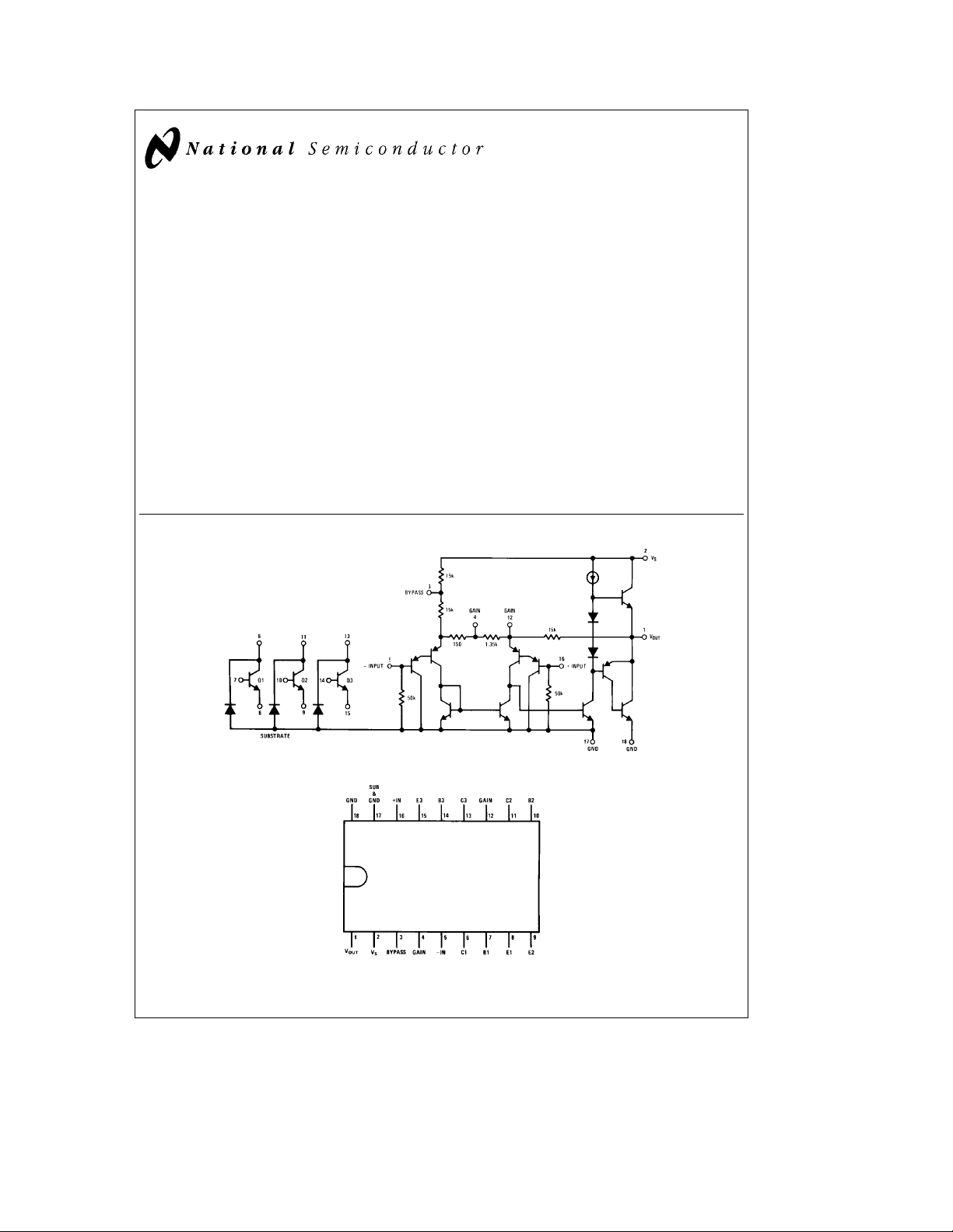
Equivalent Schematic and Connection Diagrams
Low quiescent current drain
Y
Voltage gains from 20 to 200
Y
Ground referenced input
Y
Self-centering output quiescent voltage
Y
Low distortion
Transistors
Y
Operation from 1 mAto25mA
Y
Frequency range from DC to 100 MHz
Y
Excellent matching
Applications
Y
AM-FM radios
Y
Portable tape recorders
Y
Intercoms
Y
Toys and games
Y
Walkie-talkies
Y
Portable phonographs
Y
Power converters
LM389 Low Voltage Audio Power Amplifier with NPN Transistor Array
December 1994
TL/H/7847– 1
Dual-In-Line Package
Order Number LM389N
TL/H/7847– 2
See NS Package Number N18A
C
1995 National Semiconductor Corporation RRD-B30M115/Printed in U. S. A.
TL/H/7847
Page 2
Absolute Maximum Ratings
If Military/Aerospace specified devices are required,
please contact the National Semiconductor Sales
Office/Distributors for availability and specifications.
Supply Voltage 15V
Package Dissipation (Note 1) 1.89W
Ctoa70§C
§
e
25§C
A
g
0.4V
§
§
12V
Input Voltage
Storage Temperature
b
65§Ctoa150§C
Operating Temperature 0
Junction Temperature 150
Lead Temperature (Soldering, 10 sec.) 260
Collector to Emitter Voltage, V
CEO
Electrical Characteristics T
Symbol Parameter Conditions Min Typ Max Units
AMPLIFIER
V
S
I
Q
P
OUT
A
V
BW Bandwidth V
THD Total Harmonic Distortion V
PSRR Power Supply Rejection Ratio V
R
IN
I
BIAS
Operating Supply Voltage 4 12 V
Quiescent Current V
Output Power (Note 3)
Voltage Gain V
e
S
e
THD
e
S
10 mF from Pins 4 to 12 46 dB
e
S
e
S
e
1 kHz, Pins 4 and 12 Open
f
e
S
Pins 4 and 12 Open, Referred to Output
Input Resistance 10 50 kX
Input Bias Current V
e
S
TRANSISTORS
V
CEO
V
CBO
V
CIO
V
EBO
H
FE
h
oe
V
BE
V
l
BE1–VBE2
V
CESAT
C
EB
C
CB
C
CI
h
fe
Note 1: For operation in ambient temperatures above 25§C, the device must be derated based on a 150§C maximum junction temperature and a thermal resistance
C/W junction to ambient.
of 66
§
Note 2: The collector of each transistor is isolated from the substrate by an integral diode. Therefore, the collector voltage should remain positive with respect to
pin 17 at all times.
Note 3: If oscillation exists under some load conditions, add 2.7X and 0.05 m F series network from pin 1 to ground.
Collector to Emitter I
Breakdown Voltage
Collector to Base I
Breakdown Voltage
Collector to Substrate I
Breakdown Voltage
Emitter to Base I
Breakdown Voltage
Static Forward Current I
Transfer Ratio (Static Beta) I
Open-Circuit Output Admittance I
Base to Emitter Voltage I
Base to Emitter Voltage Offset I
l
Collector to Emitter I
Saturation Voltage
Emitter to Base Capacitance V
Collector to Base Capacitance V
Collector to Substrate V
Capacitance
High Frequency Current Gain I
e
1 mA, I
C
e
10 mA, I
C
e
10 mA, I
C
e
10 mA, I
E
e
10 mA 100
C
e
1 mA 100 275
C
e
10 mA 275
I
C
e
1 mA, V
C
e
1 mA 0.7 0.85 V
E
e
1mA 1 5 mV
E
e
10 mA, I
C
e
EB
e
CB
e
CI
e
10 mA, V
C
Collector to Base Voltage, V
Collector to Substrate Voltage, V
(Note 2) 15V
Collector Current, I
Emitter Current, I
Base Current, I
Power Dissipation (Each Transistor) T
B
Thermal Resistance
C
C
6V, V
i
JC
i
JA
e
0V 6 12 mA
IN
10%
e
6V, R
V
S
e
9V, R
V
S
E
L
L
CBO
CIO
C
s
a
70§C 150 mW
A
e
8X 250 325 mW
e
16X 500 mW
25 mA
25 mA
5mA
24§C/W
70§C/W
6V, fe1 kHz 23 26 30 dB
6V, Pins 4 and 12 Open 250 kHz
e
6V, R
8X,P
L
6V, fe1 kHz, C
OUT
BYPASS
e
125 mW,
e
10 mF,
0.2 3.0 %
30 50 dB
6V, Pins 5 and 16 Open 250 nA
e
0
B
e
0
E
e
e
I
E
C
CE
B
0
B
e
0
e
5V, fe1.0 kHz 20 mmho
e
1mA
12 20 V
15 40 V
15 40 V
6.4 7.1 7.8 V
0.15 0.5 V
3V 1.5 pF
3V 2 pF
3V
e
5V, fe100 MHz 1.5 5.5
CE
3.5 pF
2
15V
Page 3
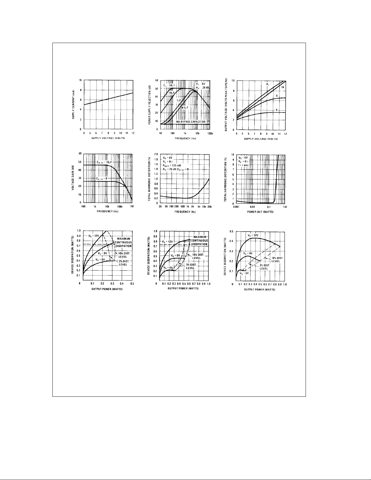
Typical Amplifier Performance Characteristics
Quiescent Supply Current
vs Supply Voltage
Voltage Gain vs Frequency Distortion vs Frequency Distortion vs Output Power
Device Dissipation vs Output
PowerÐ4X Load
Power Supply Rejection Ratio
(Referred to the Output)
vs Frequency
Device Dissipation vs Output
PowerÐ8X Load
Peak-to-Peak Output Voltage
Swing vs Supply Voltage
Device Dissipation vs Output
PowerÐ16X Load
TL/H/7847– 3
3
Page 4

Typical Transistor Performance Characteristics
Forward Current Transfer Ratio
vs Collector Current
Saturation Voltage vs
Collector Current
Open Circuit Output Admittance
vs Collector Current
High Frequency Current Gain
Noise Voltage vs Frequency Noise Current vs Frequency vs Collector Current
and Coevs Collector
g
oe
Current
goeand Coevs Collector
Current
Contours of Constant Noise
Figure
TL/H/7847– 4
TL/H/7847– 5
4
Page 5

Application Hints
Gain Control
To make the LM389 a more versatile amplifier, two pins (4
and 12) are provided for gain control. With pins 4 and 12
open, the 1.35 kX resistor sets the gain at 20 (26 dB). If a
capacitor is put from pin 4 to 12, bypassing the 1.35 kX
resistor, the gain will go up to 200 (46 dB). If a resistor is
placed in series with the capacitor, the gain can be set to
any value from 20 to 200. A low frequency pole in the gain
response is caused by the capacitor working against the
external resistor in series with the 150X internal resistor. If
the capacitor is eliminated and a resistor connects pin 4 to
12, then the output dc level may shift due to the additional
dc gain. Gain control can also be done by capacitively coupling a resistor (or FET) from pin 12 to ground.
Additional external components can be placed in parallel
with the internal feedback resistors to tailor the gain and
frequency response for individual applications. For example,
we can compensate poor speaker bass response by frequency shaping the feedback path. This is done with a series RC from pin 1 to 12 (paralleling the internal 15 kX resistor). For 6 dB effective bass boost: Rj15 kX, the lowest
value for good stable operation is R
open. If pins 4 and 12 are bypassed then R as low as 2 kX
can be used. This restriction is because the amplifier is only
compensated for closed-loop gains greater than 9V/V.
Input Biasing
The schematic shows that both inputs are biased to ground
witha50kXresistor. The base current of the input transis-
tors is about 250 nA, so the inputs are at about 12.5 mV
when left open. If the dc source resistance driving the
LM389 is higher than 250 kX it will contribute very little
additional offset (about 2.5 mV at the input, 50 mV at the
output). If the dc source resistance is less than 10 kX, then
shorting the unused input to ground will keep the offset low
(about 2.5 mV at the input, 50 mV at the output). For dc
source resistances between these values we can eliminate
excess offset by putting a resistor from the unused input to
ground, equal in value to the dc source resistance. Of
course all offset problems are eliminated if the input is capacitively coupled.
When using the LM389 with higher gains (bypassing the
1.35 kX resistor between pins 4 and 12) it is necessary to
e
10 kX if pin 4 is
bypass the unused input, preventing degradation of gain
and possible instabilities. This is done with a 0.1 mF capacitor or a short to ground depending on the dc source resistance of the driven input.
Supplies and Grounds
The LM389 has excellent supply rejection and does not require a well regulated supply. However, to eliminate possible high frequency stability problems, the supply should be
decoupled to ground with a 0.1 mF capacitor. The high current ground of the output transistor, pin 18, is brought out
separately from small signal ground, pin 17. If the two
ground leads are returned separately to supply then the parasitic resistance in the power ground lead will not cause
stability problems. The parasitic resistance in the signal
ground can cause stability problems and it should be minimized. Care should also be taken to insure that the power
dissipation does not exceed the maximum dissipation of the
package for a given temperature. There are two ways to
mute the LM389 amplifier. Shorting pin 3 to the supply voltage, or shorting pin 12 to ground will turn the amplifier off
without affecting the input signal.
Transistors
The three transistors on the LM389 are general purpose
devices that can be used the same as other small signal
transistors. As long as the currents and voltages are kept
within the absolute maximum limitations, and the collectors
are never at a negative potential with respect to pin 17,
there is no limit on the way they can be used.
For example, the emitter-base breakdown voltage of 7.1V
can be used as a zener diode at currents from 1 mAto
5 mA. These transistors make good LED driver devices,
V
is only 150 mV when sinking 10 mA.
SAT
In the linear region, these transistors have been used in AM
and FM radios, tape recorders, phonographs and many other applications. Using the characteristic curves on noise
voltage and noise current, the level of the collector current
can be set to optimize noise performance for a given source
impedance. Some of the circuits that have been built are
shown in
Figures 1–7
of applications, since that is limited only by the designers
imagination.
. This is by no means a complete list
FIGURE 1. AM Radio
5
TL/H/7847– 6
Page 6

Application Hints (Continued)
All switches in record mode
Head characteristic 280 mH/300X
FIGURE 2. Tape Recorder
FIGURE 3. Ceramic Phono Amplifier with Tone Controls
TL/H/7847– 7
TL/H/7847– 8
6
Page 7

Application Hints (Continued)
e
f
0.69R1C1
FIGURE 4. FM Scanner Noise Squelch Circuit
TL/H/7847– 9
1
TL/H/7847– 10
FIGURE 5. Siren
FIGURE 6. Voltage-Controlled Amplifier or Tremolo Circuit
7
* Tremolo freq.
s
2q (Ra10k)C
TL/H/7847– 11
1
Page 8

Application Hints (Continued)
FIGURE 7. Noise Generator Using Zener Diode
TL/H/7847– 12
Physical Dimensions inches (millimeters)
Molded Dual-In-Line Package (N)
Order Number LM389N
NS Package Number N18A
LIFE SUPPORT POLICY
LM389 Low Voltage Audio Power Amplifier with NPN Transistor Array
NATIONAL’S PRODUCTS ARE NOT AUTHORIZED FOR USE AS CRITICAL COMPONENTS IN LIFE SUPPORT
DEVICES OR SYSTEMS WITHOUT THE EXPRESS WRITTEN APPROVAL OF THE PRESIDENT OF NATIONAL
SEMICONDUCTOR CORPORATION. As used herein:
1. Life support devices or systems are devices or 2. A critical component is any component of a life
systems which, (a) are intended for surgical implant support device or system whose failure to perform can
into the body, or (b) support or sustain life, and whose be reasonably expected to cause the failure of the life
failure to perform, when properly used in accordance support device or system, or to affect its safety or
with instructions for use provided in the labeling, can effectiveness.
be reasonably expected to result in a significant injury
to the user.
National Semiconductor National Semiconductor National Semiconductor National Semiconductor
Corporation Europe Hong Kong Ltd. Japan Ltd.
1111 West Bardin Road Fax: (
Arlington, TX 76017 Email: cnjwge@tevm2.nsc.com Ocean Centre, 5 Canton Rd. Fax: 81-043-299-2408
Tel: 1(800) 272-9959 Deutsch Tel: (
Fax: 1(800) 737-7018 English Tel: (
National does not assume any responsibility for use of any circuitry described, no circuit patent licenses are implied and National reserves the right at any time without notice to change said circuitry and specifications.
Fran3ais Tel: (
Italiano Tel: (
a
49) 0-180-530 85 86 13th Floor, Straight Block, Tel: 81-043-299-2309
a
49) 0-180-530 85 85 Tsimshatsui, Kowloon
a
49) 0-180-532 78 32 Hong Kong
a
49) 0-180-532 93 58 Tel: (852) 2737-1600
a
49) 0-180-534 16 80 Fax: (852) 2736-9960
 Loading...