

Page 1
LM388 1.5W Audio Power Amplifier
Y
General Description
The LM388 is an audio amplifier designed for use in medium
power consumer applications. The gain is internally set to
20 to keep external part count low, but the addition of an
external resistor and capacitor between pins 2 and 6 will
increase the gain to any value up to 200.
The inputs are ground referenced while the output is automatically biased to one half the supply voltage.
Features
Y
Minimum external parts
Y
Wide supply voltage range
Y
Excellent supply rejection
Y
Ground referenced input
Y
Self-centering output quiescent voltage
Variable voltage gain
Y
Low distortion
Y
Fourteen pin dual-in-line package
Y
Low voltage operation, 4V
Applications
Y
AM-FM radio amplifiers
Y
Portable tape player amplifiers
Y
Intercoms
Y
TV sound systems
Y
Lamp drivers
Y
Line drivers
Y
Ultrasonic drivers
Y
Small servo drivers
Y
Power converters
LM388 1.5W Audio Power Amplifier
February 1995
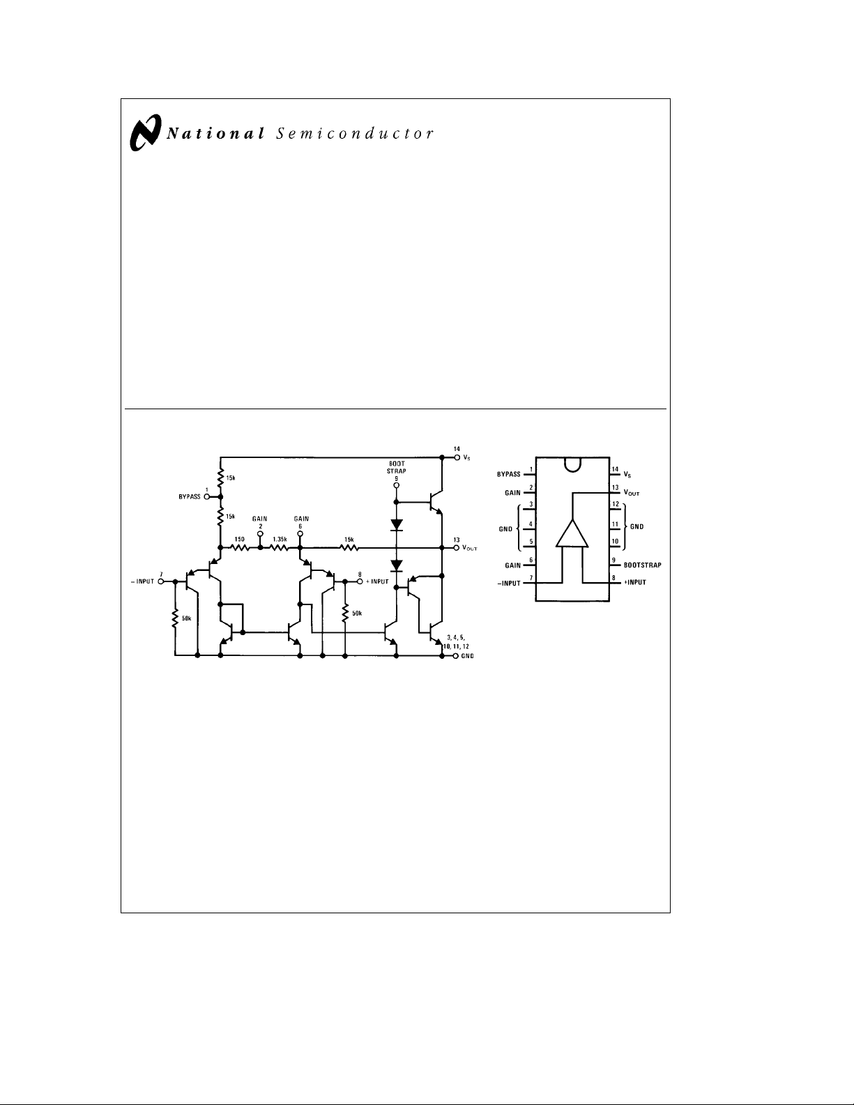
Equivalent Schematic and Connection Diagrams
TL/H/7846– 1
Dual-In-Line Package
TL/H/7846– 2
Top View
Order Number LM388N-1
See NS Package Number N14A
C
1995 National Semiconductor Corporation RRD-B30M115/Printed in U. S. A.
TL/H/7846
Page 2
Absolute Maximum Ratings
If Military/Aerospace specified devices are required,
please contact the National Semiconductor Sales
Office/Distributors for availability and specifications.
Supply Voltage 15V
Package Dissipation 14-Pin DIP (Note 1) 8.3W
Input Voltage
Storage Temperature
b
65§Ctoa150§C
g
0.4V
Operating Temperature 0
Ctoa70§C
§
Junction Temperature 150§C
Lead Temperature (Soldering, 10 sec.) 260§C
Thermal Resistance
i
JC
i
JA
30§C/W
79§C/W
Electrical Characteristics T
e
25§C,
A
(Figure 1)
Symbol Parameter Conditions Min Typ Max Units
V
S
I
Q
P
OUT
A
V
BW Bandwidth V
THD Total Harmonic Distortion V
PSRR Power Supply Rejection Ratio V
R
IN
I
BIAS
Note 1: Pins 3, 4, 5, 10, 11, 12 at 25§C. Derate at 15§C/W above 25§C case.
Note 2: The amplifier should be in high gain for full swing on higher supplies due to input voltage limitations.
Note 3: If load and bypass capacitor are returned to V
Operating Supply Voltage
LM388
Quiescent Current V
LM388 V
e
0
IN
e
12V
S
412V
16 23 mA
Output Power (Note 2) R1eR2e180X, THDe10%
LM388N-1 V
Voltage Gain V
(Note 3) Pins 2 and 6 Open, Referred to Output
e
S
e
V
S
e
S
10 mF from Pins 2 to 6 46 dB
e
S
e
S
fe1 kHz, Pins 2 and 6 Open
e
S
e
12V, R
6V, R
8X 1.5 2.2 W
L
e
4X 0.6 0.8 W
L
12V, fe1 kHz 23 26 30 dB
12V, Pins 2 and 6 Open 300 kHz
e
12V, R
8X,P
L
12V, fe1 kHz, C
OUT
BYPASS
e
500 mW,
e
10 mF,
0.1 1 %
50 dB
Input Resistance 10 50 kX
(Figure 2),
S
e
12V, Pins 7 and 8 Open 250 nA
S
rather than ground
(Figure 1),
PSRR is typically 30 dB.
Input Bias Current V
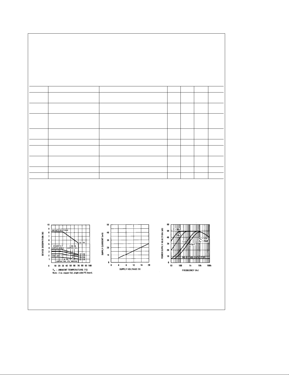
Typical Performance Characteristics
Maximum Device Dissipation vs
Ambient Temperature
Quiescent Supply Current vs
Supply Voltage
Power Supply Rejection Ratio
(Referred to the Output) vs
Frequency
TL/H/7846– 5
2
Page 3
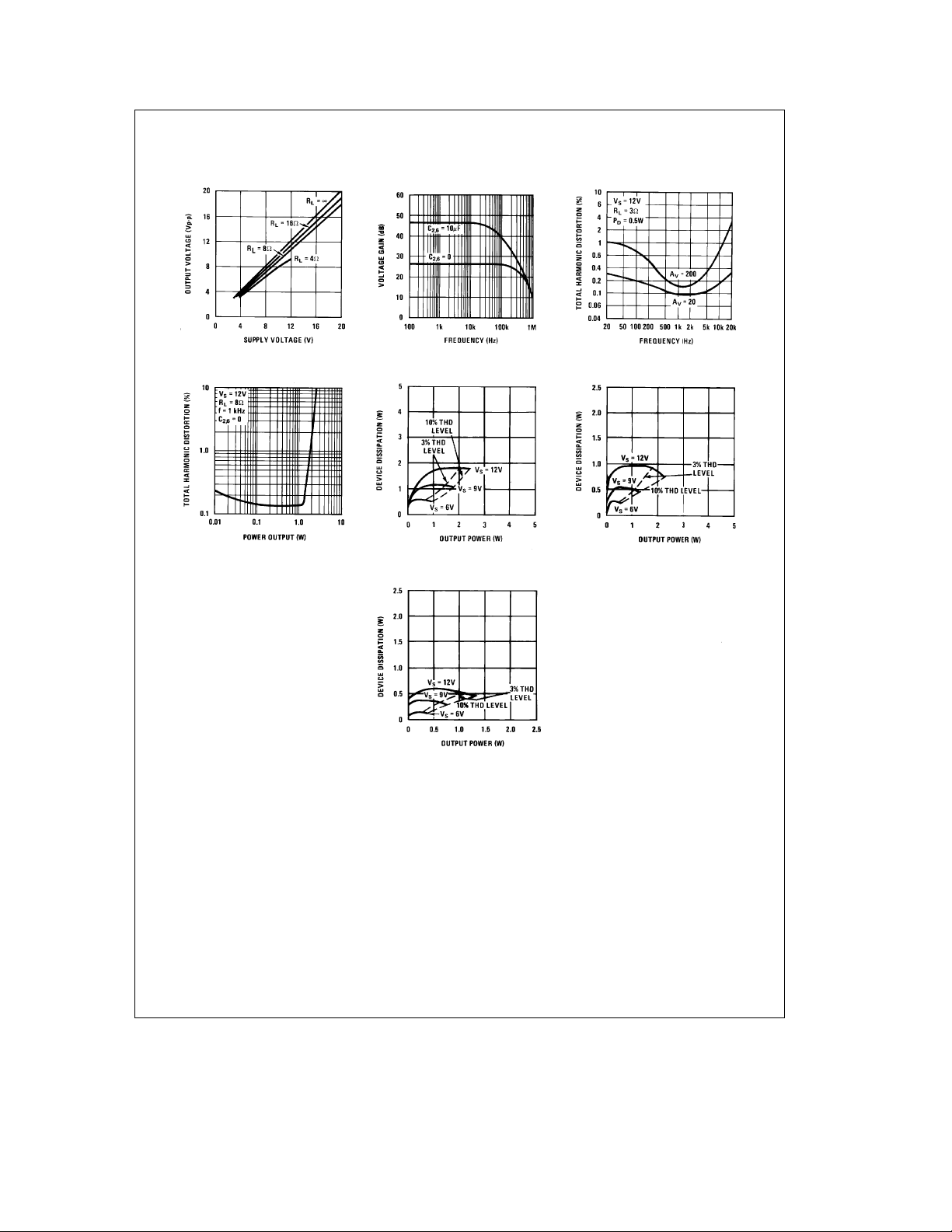
Typical Performance Characteristics (Continued)
Peak-to-Peak Output Voltage
Swing vs Supply Voltage
Voltage Gain vs Frequency Distortion vs Frequency
Distortion vs Output Power PowerÐ4X Load
Device Dissipation vs Output
Device Dissipation vs
Output PowerÐ16X Load
Application Hints
GAIN CONTROL
To make the LM388 a more versatile amplifier, two pins (2
and 6) are provided for gain control. With pins 2 and 6 open,
the 1.35 kX resistor sets the gain at 20 (26 dB). If a capacitor is put from pins 2 to 6, bypassing the 1.35 kX resistor,
the gain will go up to 200 (46 dB). If a resistor is placed in
series with the capacitor, the gain can be set to any value
from 20 to 200. A low frequency pole in the gain response is
caused by the capacitor working against the external resistor in series with the 150X internal resistor. If the capacitor
is eliminated and a resistor connects pins 2 to 6 then the
Device Dissipation vs
Output PowerÐ8X Load
TL/H/7846– 6
output dc level may shift due to the additional dc gain. Gain
control can also be done by capacitively coupling a resistor
(or FET) from pin 6 to ground, as in
Additional external components can be placed in parallel
with the internal feedback resistors to tailor the gain and
frequency response for individual applications. For example,
we can compensate poor speaker bass response by frequency shaping the feedback path. This is done with a series RC from pin 6 to 13 (paralleling the internal 15 kX resistor). For 6 dB effective bass boost: Rj15 kX, the lowest
value for good stable operation is R
Figure 7
e
.
10 kX if pin 2
3
Page 4

Application Hints (Continued)
is open. If pins 2 and 6 are bypassed then R as low as 2 kX
can be used. This restriction is because the amplifier is only
compensated for closed-loop gains greater than 9 V/V.
INPUT BIASING
The schematic shows that both inputs are biased to ground
witha50kXresistor . The base current of the input transis-
tors is about 250 nA, so the inputs are at about 12.5 mV
when left open. If the dc source resistance driving the
LM388 is higher than 250 kX it will contribute very little
additional offset (about 2.5 mV at the input, 50 mV at the
output). If the dc source resistance is less than 10 kX, then
shorting the unused input to ground will keep the offset low
(about 2.5 mV at the input, 50 mV at the output). For dc
source resistances between these values we can eliminate
excess offset by putting a resistor from the unused input to
ground, equal in value to the dc source resistance. Of
course all offset problems are eliminated if the input is capacitively coupled.
When using the LM388 with higher gains (bypassing the
1.35 kX resistor between pins 2 and 6) it is necessary to
bypass the unused input, preventing degradation of gain
and possible instabilities. This is done with a 0.1 mF capacitor or a short to ground depending on the dc source resistance on the driven input.
BOOTSTRAPPING
The base of the output transistor of the LM388 is brought
out to pin 9 for Bootstrapping. The output stage of the amplifier during positive swing is shown in
external circuitry.
a
R1
R2 set the amount of base current available to the
output transistor. The maximum output current divided by
Figure 3
with its
beta is the value required for the current in R1 and R2:
BE
2P
e
0
(12/2)b0.7
#
4C
j
B
b
(VS/2)bV
O
e
0.7V and b
O
R
L
0.5
c
j
O
L
a
(R1
R2)eb
Good design values are V
Example: 1 watt into 8X load with V
I
O MAX
a
R2)e100
(R1
To keep the current in R2 constant during positive swing
capacitor C
R1 and R2 above the supply, maintaining a constant voltage
across R2. To minimize the value of C
due to C
due to the output coupling capacitor and the load. This
gives:
Example: for 100 Hz pole and R
e
C
B
the same current, C
4, as in
For reduced component count the load can replace R1. The
value of (R1
is both the coupling and the bootstrapping capacitor (see
Figure 2
is added. As the output swings positive CBlifts
B
and R1 and R2 is usually set equal to the pole
B
C
8 mF, if R1 is made a diode and R2 increased to give
Figure 4
).
can be decreased by about a factor of
B
.
a
R2) is the same, so R2 is increased. Now C
BE
I
O MAX
e
O
e
12V.
S
e
500 mA
e
1060X
J
,R1eR2. The pole
B
C
c
25
e
8X;C
e
c
100.
200 mF and
B
Typical Applications
FIGURE 1. Load Returned to Ground
(Amplifier with Gain
TL/H/7846– 3
e
20)
4
FIGURE 2. Load Returned to V
(Amplifier with Gaine20)
TL/H/7846– 4
S
Page 5

Typical Applications (Continued)
FIGURE 3
e
V
6V R
S
e
V
12V R
S
TL/H/7846– 7
e
4X P
L
e
8X P
L
FIGURE 5. Bridge Amp
FIGURE 4. Ampifier with Gaine200 and Minimum C
TL/H/7846– 8
e
1.0W
O
e
4W
O
TL/H/7846– 9
B
FIGURE 6a. Amplifier with Bass Boost
FIGURE 6b. Frequency Response
TL/H/7846– 11
TL/H/7846– 10
with Bass Boost
5
Page 6

Typical Applications (Continued)
FIGURE 7. Intercom
FIGURE 8. AM Radio Power Amplifier
Note 1: Twist supply lead and supply ground very tightly.
Note 2: Twist speaker lead and ground very tightly.
Note 3: Ferrite bead is Ferroxcube K5-001-001/3B with 3 turns of wire.
TL/H/7846– 12
TL/H/7846– 13
Note 4: R1C1 band limits input signals.
Note 5: All components must be spaced very close to IC.
6
Page 7

7
Page 8

Physical Dimensions inches (millimeters)
LM388 1.5W Audio Power Amplifier
Molded Dual-In-Line Package (N)
Order Number LM388N-1
NS Package Number N14A
LIFE SUPPORT POLICY
NATIONAL’S PRODUCTS ARE NOT AUTHORIZED FOR USE AS CRITICAL COMPONENTS IN LIFE SUPPORT
DEVICES OR SYSTEMS WITHOUT THE EXPRESS WRITTEN APPROVAL OF THE PRESIDENT OF NATIONAL
SEMICONDUCTOR CORPORATION. As used herein:
1. Life support devices or systems are devices or 2. A critical component is any component of a life
systems which, (a) are intended for surgical implant support device or system whose failure to perform can
into the body, or (b) support or sustain life, and whose be reasonably expected to cause the failure of the life
failure to perform, when properly used in accordance support device or system, or to affect its safety or
with instructions for use provided in the labeling, can effectiveness.
be reasonably expected to result in a significant injury
to the user.
National Semiconductor National Semiconductor National Semiconductor National Semiconductor
Corporation Europe Hong Kong Ltd. Japan Ltd.
1111 West Bardin Road Fax: (
Arlington, TX 76017 Email: cnjwge@tevm2.nsc.com Ocean Centre, 5 Canton Rd. Fax: 81-043-299-2408
Tel: 1(800) 272-9959 Deutsch Tel: (
Fax: 1(800) 737-7018 English Tel: (
National does not assume any responsibility for use of any circuitry described, no circuit patent licenses are implied and National reserves the right at any time without notice to change said circuitry and specifications.
Fran3ais Tel: (
Italiano Tel: (
a
49) 0-180-530 85 86 13th Floor, Straight Block, Tel: 81-043-299-2309
a
49) 0-180-530 85 85 Tsimshatsui, Kowloon
a
49) 0-180-532 78 32 Hong Kong
a
49) 0-180-532 93 58 Tel: (852) 2737-1600
a
49) 0-180-534 16 80 Fax: (852) 2736-9960
 Loading...