

Page 1
March 2007
LM3880
Power Sequencer
General Description
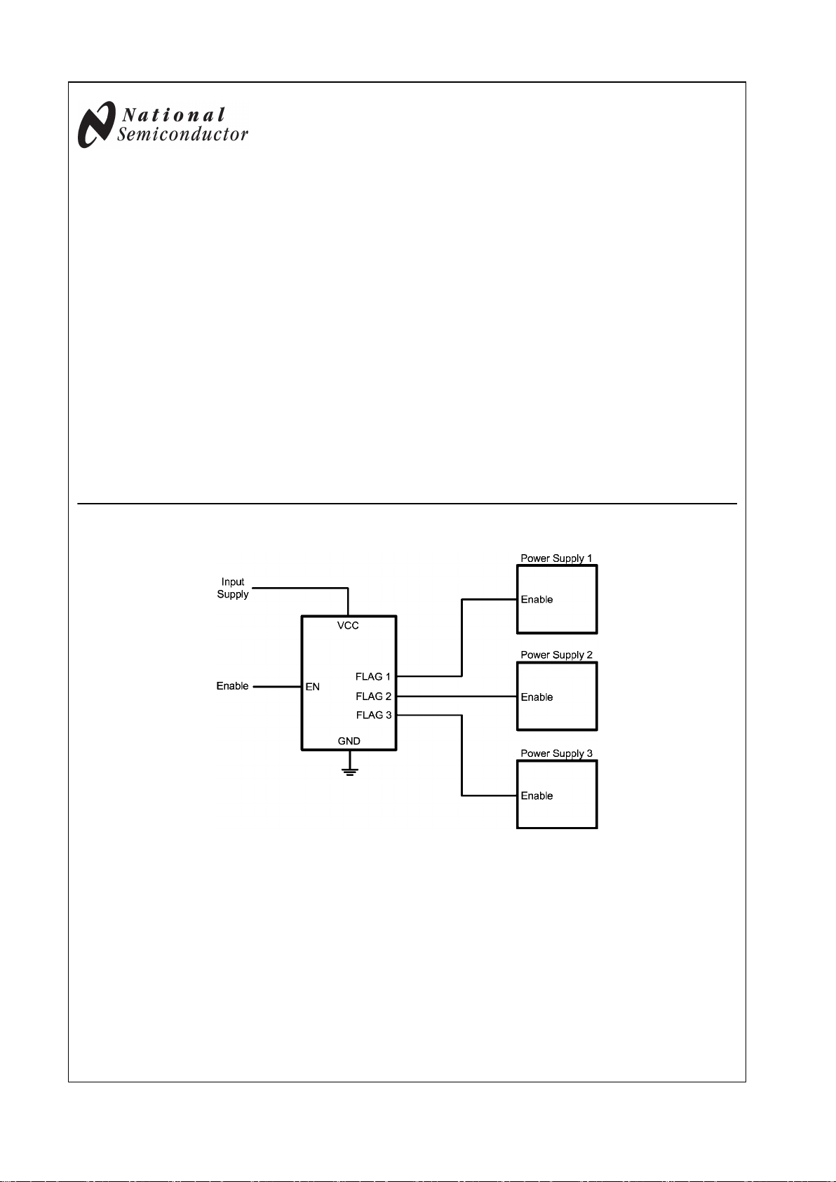
The LM3880 Power Sequencer offers the easiest method to
control power up and power down of multiple power supplies
(switchers or linear regulators). By staggering the startup sequence, it is possible to avoid latch conditions or large in-rush
currents that can affect the reliability of the system.
Available in a SOT23-6 package, the Power Sequencer contains a precision enable pin and three open drain output flags.
Upon enabling the LM3880 the three output flags will sequentially release, after individual time delays, permitting the connected power supplies to startup. The output flags will follow
a reverse sequence during power down to avoid latch conditions.
Standard timing option of 30ms is available.
EPROM capability allows every delay and sequence to be
fully adjustable. Contact National Semiconductor if a nonstandard configuration is required.
Features
■
Easiest method to sequence rails
■
Power up and power down control
■
Input voltage range of 2.7V to 5.5V
■
Small footprint SOT23-6
■
Low quiescent current of 25 µA
■
Standard timing options available
■
Customization of timing and sequence available through
factory programmability
Applications
■
Multiple supply sequencing
■
Microprocessor / Microcontroller sequencing
■
FPGA sequencing
Typical Application Circuit
20192601
© 2007 National Semiconductor Corporation 201926 www.national.com
LM3880 Power Sequencer
Page 2
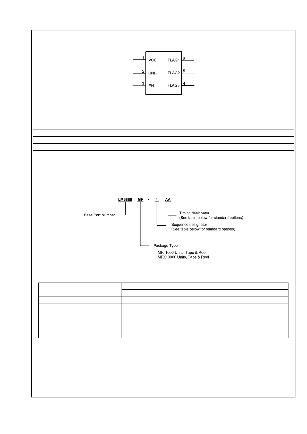
Connection Diagram
20192602
Top View
SOT23–6 Package
Pin Descriptions
Pin # Name Function
1 VCC Input supply
2 GND Ground
3 EN Precision enable pin
4 FLAG3 Open drain output #3
5 FLAG2 Open drain output #2
6 FLAG1 Open drain output #1
Ordering Information
20192603
Sequence Designator Table
Sequence Number Flag Order
Power Up Power Down
1 1 - 2 - 3 3 - 2 - 1
2 1 - 2 - 3 3 - 1 - 2
3 1 - 2 - 3 2 - 3 - 1
4 1 - 2 - 3 2 - 1 - 3
5 1 - 2 - 3 1 - 3 - 2
6 1 - 2 - 3 1 - 2 - 3
See timing diagrams for more information
www.national.com 2
LM3880
Page 3
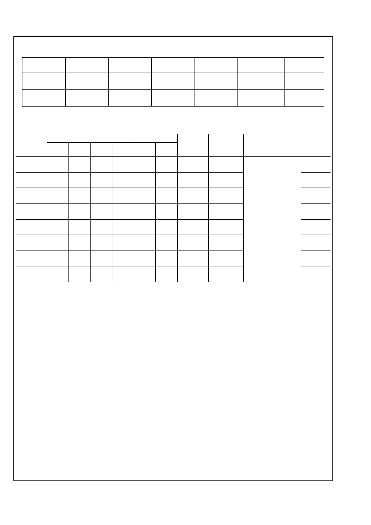
Timing Designator Table
Timing
Designator
t
d1
t
d2
t
d3
t
d4
t
d5
t
d6
AA 10ms 10ms 10ms 10ms 10ms 10ms
AB 30ms 30ms 30ms 30ms 30ms 30ms
AC 60ms 60ms 60ms 60ms 60ms 60ms
AD 120ms 120ms 120ms 120ms 120ms 120ms
See timing diagrams for more information
LM3880 Ordering Information
Order
Number
Timer settings Sequence
Order
Supplied As
Package
Type
NSC
Package
Drawing
Package
Marking
t
d1
t
d2
t
d3
t
d4
t
d5
t
d6
LM3880
MF-1AA
10ms 10ms 10ms 10ms 10ms 10ms 1 1k units T&R
SOT23-6 MF06A
F20A
LM3880
MFX-1AA
10ms 10ms 10ms 10ms 10ms 10ms 1 3k units T&R F20A
LM3880
MF-1AB
30ms 30ms 30ms 30ms 30ms 30ms 1 1k units T&R F21A
LM3880
MFX-1AB
30ms 30ms 30ms 30ms 30ms 30ms 1 3k units T&R F21A
LM3880
MF-1AC
60ms 60ms 60ms 60ms 60ms 60ms 1 1k units T&R F22A
LM3880
MFX-1AC
60ms 60ms 60ms 60ms 60ms 60ms 1 3k units T&R F22A
LM3880
MF-1AD
120ms 120ms 120ms 120ms 120ms 120ms 1 1k units T&R F23A
LM3880
MFX-1AD
120ms 120ms 120ms 120ms 120ms 120ms 1 3k units T&R F23A
Non-standard parts are available upon request. Please contact National Semiconductor for more information.
3 www.national.com
LM3880
Page 4
Absolute Maximum Ratings (Note 1)
If Military/Aerospace specified devices are required,
please contact the National Semiconductor Sales Office/
Distributors for availability and specifications.
VCC −0.3V to +6.0V
EN, FLAG1, FLAG2, FLAG3 −0.3V to 6.0V
Max Flag 'ON' Current 50 mA
Storage Temperature Range −65°C to +150°C
Junction Temperature 150°C
Lead Temperature (Soldering, 5
sec.) 260°C
Minimum ESD Rating ±2 kV
Operating Ratings (Note 1)
VCC to GND 2.7V to 5.5V
EN, FLAG1, FLAG2, FLAG3 −0.3V to VCC + 0.3V
Junction Temperature −40°C to +125°C
Electrical Characteristics Specifications with standard typeface are for T
J
= 25°C, and those in bold face type
apply over the full Operating Temperature Range (TJ = -40°C to +125°C). Minimum and Maximum limits are guaranteed through
test, design or statistical correlation. Typical values represent the most likely parametric norm at TJ = 25°C and are provided for
reference purposes only. Unless otherwise specified VCC = 3.3V.
Symbol Parameter Conditions Min
(Note 3)
Typ
(Note 4)
Max
(Note 3)
Unit
I
Q
Operating Quiescent current 25 80 µA
Open Drain Flags
I
FLAG
FLAGx Leakage Current V
FLAGx
= 3.3V 1 20 nA
V
OL
FLAGx Output Voltage Low I
FLAGx
= 1.2mA 0.4 V
Power Up Sequence
t
d1
Timer delay 1 accuracy -15 15 %
t
d2
Timer delay 2 accuracy -15 15 %
t
d3
Timer delay 3 accuracy -15 15 %
Power Down Sequence
t
d4
Timer delay 4 accuracy -15 _ 15 %
t
d5
Timer delay 5 accuracy -15 15 %
t
d6
Timer delay 6 accuracy -15 15 %
Timing Delay Error
(t
d(x)
– 400 us) / t
d(x+1)
Ratio of timing delays For x = 1 or 4 95 105 %
t
d(x)
/ t
d(x+1)
Ratio of timing delays For x = 2 or 5 95 105 %
ENABLE Pin
V
EN
EN pin threshold 1.0 1.25 1.4 V
I
EN
EN pin pull-up current VEN = 0V 7 µA
Note 1: Absolute Maximum Ratings indicate limits beyond which damage to the device may occur. Operating Ratings indicate conditions for which the device is
intended to be functional, but does not guarantee specific performance limits. For guaranteed specifications and conditions, see the Electrical Characteristics.
Note 2: The human body model is a 100 pF capacitor discharged through a 1.5 kΩ resistor into each pin.
Note 3: Limits are 100% production tested at 25°. Limits over the operating temperature range are guaranteed through correlation using Statistical Quality Control
(SQC) methods. The limits are used to calculate National's Average Outgoing Quality Level (AOQL).
Note 4: Typical numbers are at 25°C and represent the most likely parametric norm.
www.national.com 4
LM3880
Page 5

Typical Performance Characteristics
Quiescent Current vs VCC
20192604
Quiescent Current vs Temperature (VCC = 3.3V)
20192605
Enable Threshold vs Temperature
20192606
Time Delay (30ms) vs VCC
20192607
Time Delay Ratio vs Temperature
20192608
Time Delay (30ms) vs Temperature
20192609
5 www.national.com
LM3880
Page 6

FLAG VOL vs VCC
(R
FLAG
= 100 kΩ)
20192610
FLAG Voltage vs Current
20192611
Block Diagram
Block Diagram
20192612
www.national.com 6
LM3880
Page 7

Timing Diagrams (Sequence 1)
All standard options use this sequence for output flags rise and fall order.
20192613
Power Up Sequence
20192614
Power Down Sequence
Application Information
OVERVIEW
The LM3880 Power Sequencer provides an easy solution for
sequencing multiple rails in a controlled manner. Six independent timers are integrated to control the timing sequence
(power up and power down) of three open drain output flags.
These flags permit connection to either a shutdown / enable
pin of linear regulators and switchers to control the power
supplies’ operation. This allows a complete power system to
be designed without worrying about large in-rush currents or
latch-up conditions that can occur.
The timing sequence of the LM3880 is controlled entirely by
the enable (EN) pin. Upon power up, all the flags are held low
until this precision enable is pulled high. After the EN pin is
asserted, the power up sequence will commence. An internal
counter will delay the first flag (FLAG1) from rising until a fixed
time period has expired. Upon the release of the first flag another timer will begin to delay the release of the second flag
(FLAG2). This process repeats until all three flags have sequentially been released. The three timers that control the
delays are all independent of each other and can be individually programmed if needed. (See custom sequencer section).
The power down sequence is the same as power-up, but in
reverse. When EN pin is de-asserted a timer will begin that
delays the third flag (FLAG3) from pulling low. The second
and first flag will then follow in a sequential manner after their
appropriate delays. The three timers that are used to control
the power down scheme can also be individually programmed
and are completely independent of the power up timers.
Additional sequence patterns are also available in addition to
customizable timers. For more information see the custom
sequencer section.
PART OPERATION
The timing sequence of the LM3880 is controlled by the assertion of the enable signal. The enable pin is designed with
an internal comparator, referenced to a bandgap voltage
(1.25V), to provide a precision threshold. This allows a delayed timing to be externally set using a capacitor or to start
the sequencing based on a certain event, such as a line voltage reaching 90% of nominal. For an additional delayed
sequence from the rail powering VCC, simply attach a capacitor to the EN pin as shown below.
7 www.national.com
LM3880
Page 8

20192615
Cap Timing
Using the internal pull-up current source to charge the external capacitor (CEN) the enable pin delay can be calculated by
the equation below:
A resistor divider can also be used to enable the LM3880
based on a certain voltage threshold. Care needs to be taken
when sizing the resistor divider to include the effects of the
internal current source.
One of the features of the enable pin is that it provides glitch
free operation. The first timer will start counting at a rising
threshold, but will always reset if the enable pin is de-asserted
before the first output flag is released. This can be shown in
the timing diagram below:
20192617
EN Glitch
If the enable signal remains high for the entire power-up sequence, then the part will operate as shown in the standard
timing diagrams. However, if the enable signal is de-asserted
before the power-up sequence is completed the part will enter
a controlled shutdown. This allows the system to walk through
a controlled power cycling, preventing any latch conditions
from occuring. This state only occurs if the enable pin is deasserted after the completion of timer 1, but before the entire
power-up sequence is completed.
When this event occurs, the falling edge of enable pin resets
the current timer and will allow the remaining power-up cycle
to complete before beginning the power down sequence. The
power down sequence starts approximately 120ms after the
final power-up flag. This allows output voltages in the system
to stabilize before everything is shutdown. An example of this
operation can be seen below:
20192618
Incomplete Sequence
All the internal timers are generated by a master clock that
has an extremely low tempco. This allows for tight accuracy
across temperature and a consistent ratio between the individual timers. There is a slight additional delay of approxi-
mately 400 µs to timers 1 and 4 which is a result of the
EPROM refresh. This refresh time is in addition to the programmed delay time and will be almost insignificant to all but
the shortest of timer delays.
www.national.com 8
LM3880
Page 9

CUSTOM SEQUENCER
The LM3880 Power Sequencer is based on a CMOS process
utilizing an EPROM that has the capability to be custom programmed at the factory. Approximately 500,000,000 different
options are available allowing even the most complex system
to be simply sequenced. Because of the vast options that are
possible, customization is limited to orders of a certain quan-
tity. Please contact National Semiconductor for more information.
The variables that can be programmed include the six delay
timers and the reverse sequence order. For the timers, each
can be individually selected from one of the timer selector
columns in the table shown below. However, all six time delays must be from the same column.
Timer Options 1 Timer Options 2 Timer Options 3 Timer Options 4
0 0 0 0
2 4 6 8
4 8 12 16
6 12 18 24
8 16 24 32
10 20 30 40
12 24 36 48
14 28 42 56
16 32 48 64
18 36 54 72
20 40 60 80
22 44 66 88
24 48 72 96
26 52 78 104
28 56 84 112
30 60 90 120
All times listed are in milliseconds
The sequencing order for power up is always controlled by
layout. The flag number translates directly into the sequence
order during power up (ie FLAG1 will always be first). However, for some systems a different power down order could
be required. To allow flexibility for this aspect in a design, the
Power Sequencer incorporates six different options for controlling the power down sequence. These options can be seen
in the timing diagrams on the next page. This ability can be
programmed in addition to the custom timers.
9 www.national.com
LM3880
Page 10

20192619
Power Down Sequence Options
www.national.com 10
LM3880
Page 11

Physical Dimensions inches (millimeters) unless otherwise noted
SOT23-6 Package
NS Package Number MF06A
11 www.national.com
LM3880
Page 12

Notes
LM3880 Power Sequencer
THE CONTENTS OF THIS DOCUMENT ARE PROVIDED IN CONNECTION WITH NATIONAL SEMICONDUCTOR CORPORATION
(“NATIONAL”) PRODUCTS. NATIONAL MAKES NO REPRESENTATIONS OR WARRANTIES WITH RESPECT TO THE ACCURACY
OR COMPLETENESS OF THE CONTENTS OF THIS PUBLICATION AND RESERVES THE RIGHT TO MAKE CHANGES TO
SPECIFICATIONS AND PRODUCT DESCRIPTIONS AT ANY TIME WITHOUT NOTICE. NO LICENSE, WHETHER EXPRESS,
IMPLIED, ARISING BY ESTOPPEL OR OTHERWISE, TO ANY INTELLECTUAL PROPERTY RIGHTS IS GRANTED BY THIS
DOCUMENT.
TESTING AND OTHER QUALITY CONTROLS ARE USED TO THE EXTENT NATIONAL DEEMS NECESSARY TO SUPPORT
NATIONAL’S PRODUCT WARRANTY. EXCEPT WHERE MANDATED BY GOVERNMENT REQUIREMENTS, TESTING OF ALL
PARAMETERS OF EACH PRODUCT IS NOT NECESSARILY PERFORMED. NATIONAL ASSUMES NO LIABILITY FOR
APPLICATIONS ASSISTANCE OR BUYER PRODUCT DESIGN. BUYERS ARE RESPONSIBLE FOR THEIR PRODUCTS AND
APPLICATIONS USING NATIONAL COMPONENTS. PRIOR TO USING OR DISTRIBUTING ANY PRODUCTS THAT INCLUDE
NATIONAL COMPONENTS, BUYERS SHOULD PROVIDE ADEQUATE DESIGN, TESTING AND OPERATING SAFEGUARDS.
EXCEPT AS PROVIDED IN NATIONAL’S TERMS AND CONDITIONS OF SALE FOR SUCH PRODUCTS, NATIONAL ASSUMES NO
LIABILITY WHATSOEVER, AND NATIONAL DISCLAIMS ANY EXPRESS OR IMPLIED WARRANTY RELATING TO THE SALE
AND/OR USE OF NATIONAL PRODUCTS INCLUDING LIABILITY OR WARRANTIES RELATING TO FITNESS FOR A PARTICULAR
PURPOSE, MERCHANTABILITY, OR INFRINGEMENT OF ANY PATENT, COPYRIGHT OR OTHER INTELLECTUAL PROPERTY
RIGHT.
LIFE SUPPORT POLICY
NATIONAL’S PRODUCTS ARE NOT AUTHORIZED FOR USE AS CRITICAL COMPONENTS IN LIFE SUPPORT DEVICES OR
SYSTEMS WITHOUT THE EXPRESS PRIOR WRITTEN APPROVAL OF THE CHIEF EXECUTIVE OFFICER AND GENERAL
COUNSEL OF NATIONAL SEMICONDUCTOR CORPORATION. As used herein:
Life support devices or systems are devices which (a) are intended for surgical implant into the body, or (b) support or sustain life and
whose failure to perform when properly used in accordance with instructions for use provided in the labeling can be reasonably expected
to result in a significant injury to the user. A critical component is any component in a life support device or system whose failure to perform
can be reasonably expected to cause the failure of the life support device or system or to affect its safety or effectiveness.
National Semiconductor and the National Semiconductor logo are registered trademarks of National Semiconductor Corporation. All other
brand or product names may be trademarks or registered trademarks of their respective holders.
Copyright© 2007 National Semiconductor Corporation
For the most current product information visit us at www.national.com
National Semiconductor
Americas Customer
Support Center
Email:
new.feedback@nsc.com
Tel: 1-800-272-9959
National Semiconductor Europe
Customer Support Center
Fax: +49 (0) 180-530-85-86
Email: europe.support@nsc.com
Deutsch Tel: +49 (0) 69 9508 6208
English Tel: +49 (0) 870 24 0 2171
Français Tel: +33 (0) 1 41 91 8790
National Semiconductor Asia
Pacific Customer Support Center
Email: ap.support@nsc.com
National Semiconductor Japan
Customer Support Center
Fax: 81-3-5639-7507
Email: jpn.feedback@nsc.com
Tel: 81-3-5639-7560
www.national.com
 Loading...