

Page 1
LM387/LM387A Low Noise Dual Preamplifier
LM387/LM387A Low Noise Dual Preamplifier
March 1987
General Description
The LM387 is a dual preamplifier for the amplification of low
level signals in applications requiring optimum noise performance. Each of the two amplifiers is completely independent, with an internal power supply decoupler-regulator, providing 110 dB supply rejection and 60 dB channel separation. Other outstanding features include high gain (104 dB),
large output voltage swing (V
bandwidth (75 kHz, 20 Vp-p). The LM387A is a selected
b
2V)p-p, and wide power
CC
version of the LM387 that has lower noise in a NAB tape
circuit, and can operate on a larger supply voltage. The
LM387 operates from a single supply across the wide range
of 9V to 30V, the LM387A operates on a supply of 9V to
40V.
The amplifiers are internally compensated for gains greater
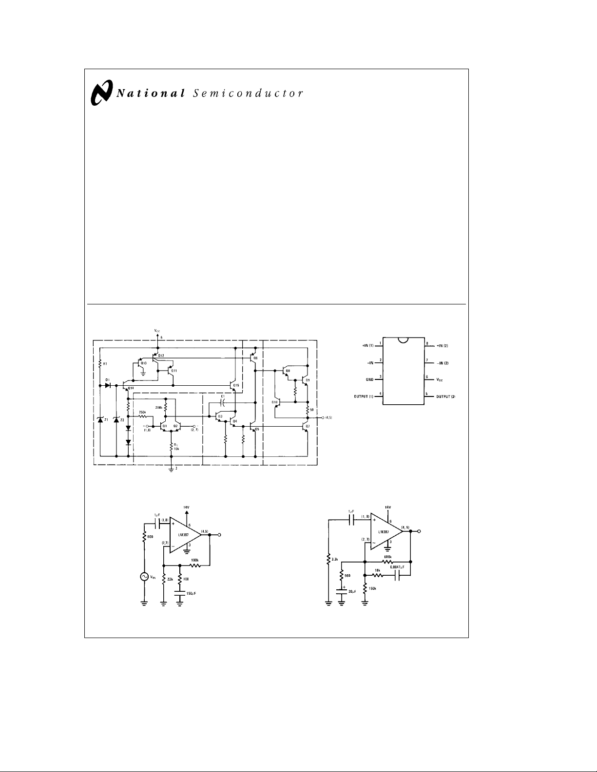
than 10. The LN387, LM387A is available in an 8-lead dualin-line package. The LM387, LM387A is biased like the
LM381. See AN-64 and AN-104.
Schematic and Connection Diagrams
Features
Y
Low noise 1.0 mV total input noise
Y
High gain 104 dB open loop
Y
Single supply operation
Y
Wide supply range LM387 9 to 30V
Y
Power supply rejection 110 dB
Y
Large output voltage swing (V
Y
Wide bandwidth 15 MHz unity gain
Y
Power bandwidth 75 kHz, 20 Vp-p
Y
Internally compensated
Y
Short circuit protected
Y
Performance similar to LM381
LM387A 9 to 40V
b
2V)p-p
CC
Dual-In-Line Package
Top View
TL/H/7845– 2
Order Number LM387N or LM387AN
See NS Package Number N08E
TL/H/7845– 1
Typical Applications
TL/H/7845– 3
FIGURE 1. Flat Gain Circuit (A
C
1995 National Semiconductor Corporation RRD-B30M115/Printed in U. S. A.
TL/H/7845
e
1000)
V
FIGURE 2. NAB Tape Circuit
TL/H/7845– 4
Page 2
Absolute Maximum Ratings
If Military/Aerospace specified devices are required,
please contact the National Semiconductor Sales
Office/Distributors for availability and specifications.
Supply Voltage
LM387
LM387A
a
30V
a
40V
Power Dissipation (Note 1) 1.5W
Operating Temperature Range 0
Storage Temperature Range
Ctoa70§C
§
b
65§Ctoa150§C
Lead Temperature (Soldering, 10 sec.) 260§C
Electrical Characteristics T
e
25§C, V
A
e
14V, unless otherwise stated
CC
Parameter Conditions Min Typ Max Units
Voltage Gain Open Loop, fe100 Hz 160,000 V/V
Supply Current LM387, VCC9V–30V, R
Input Resistance
Positive Input 50 100 kX
Negative Input 200 kX
Input Current
Negative Input
LM387A, V
9V–40V, R
CC
L
e %
e %
L
10 mA
10 mA
0.5 3.1 mA
Output Resistance Open Loop 150 X
Output Current Source 8 mA
Output Voltage Swing Peak-to-Peak V
Sink 2 mA
b
2V
CC
Unity Gain Bandwidth 15 MHz
Large Signal Frequency 20 Vp-p (V
Response THD
l
24V),
CC
s
1%
75 kHz
Maximum Input Voltage Linear Operation 300 mVrms
Supply Rejection Ratio fe1 kHz
Input Referred
110 dB
Channel Separation fe1 kHz 40 60 dB
Total Harmonic Distortion 60 dB Gain, fe1 kHz 0.1 0.5 %
Total Equivalent Input 10 Hz – 10,000 Hz
Noise (Flat Gain Cricuit) LM387
Output Noise NAB Tape Unweighted
Playback Circuit Gain of 37 dB LM387A
Note 1: For operation in ambient temperatures above 25§C, the device must be derated based on a 150§C maximum junction temperature and a thermal resistance
C/W junction to ambient.
of 80
§
Figure 1
Figure 2
1.0 1.2 mVrms
400 700 mVrms
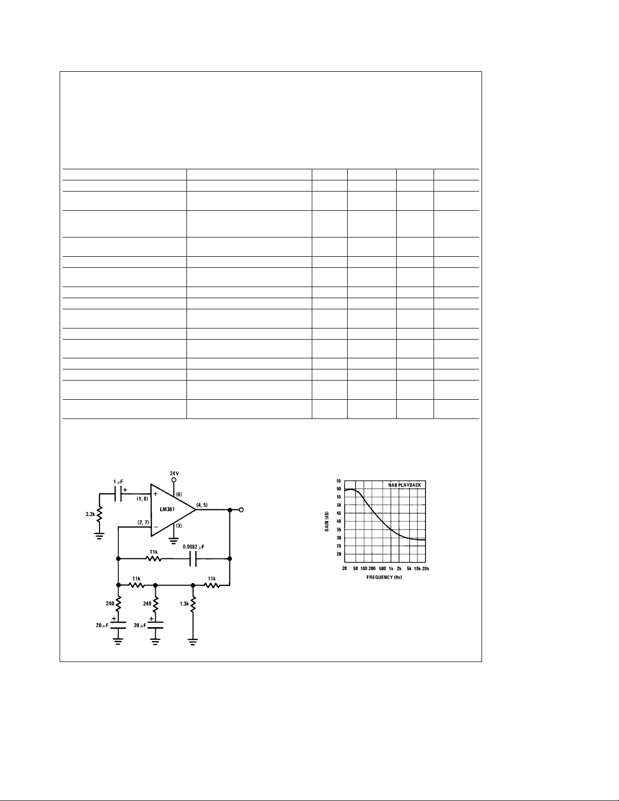
Typical Applications (Continued)
Two-Pole Fast Turn-ON NAB Tape Preamplifier
Frequency Response of NAB
Circuit of Figure 2
TL/H/7845– 5
TL/H/7845– 6
2
Page 3

Typical Performance Characteristics
VCCvs I
CC
PSRR vs Frequency
(Input Referred)
Noise Voltage vs
Frequency
Gain and Phase Response Response
Channel Separation Non-Inverting Amplifier
Noise Current vs
Frequency
Large Signal Frequency
Distortion vs Frequency
Distortion vs Frequency
Inverting Amplifier
TL/H/7845– 7
3
Page 4

Typical Applications (Continued)
Inverting Amplifier Ultra-Low Distortion
Physical Dimensions inches (millimeters)
Molded Dual-In-Line Package (N)
Order Number LM387N or LM387AN
NS Package Number N08E
LM387/LM387A Low Noise Dual Preamplifier
Typical Magnetic Phono Preamplifier
TL/H/7845– 8
TL/H/7845– 9
LIFE SUPPORT POLICY
NATIONAL’S PRODUCTS ARE NOT AUTHORIZED FOR USE AS CRITICAL COMPONENTS IN LIFE SUPPORT
DEVICES OR SYSTEMS WITHOUT THE EXPRESS WRITTEN APPROVAL OF THE PRESIDENT OF NATIONAL
SEMICONDUCTOR CORPORATION. As used herein:
1. Life support devices or systems are devices or 2. A critical component is any component of a life
systems which, (a) are intended for surgical implant support device or system whose failure to perform can
into the body, or (b) support or sustain life, and whose be reasonably expected to cause the failure of the life
failure to perform, when properly used in accordance support device or system, or to affect its safety or
with instructions for use provided in the labeling, can effectiveness.
be reasonably expected to result in a significant injury
to the user.
National Semiconductor National Semiconductor National Semiconductor National Semiconductor
Corporation Europe Hong Kong Ltd. Japan Ltd.
1111 West Bardin Road Fax: (
Arlington, TX 76017 Email: cnjwge@tevm2.nsc.com Ocean Centre, 5 Canton Rd. Fax: 81-043-299-2408
Tel: 1(800) 272-9959 Deutsch Tel: (
Fax: 1(800) 737-7018 English Tel: (
National does not assume any responsibility for use of any circuitry described, no circuit patent licenses are implied and National reserves the right at any time without notice to change said circuitry and specifications.
Fran3ais Tel: (
Italiano Tel: (
a
49) 0-180-530 85 86 13th Floor, Straight Block, Tel: 81-043-299-2309
a
49) 0-180-530 85 85 Tsimshatsui, Kowloon
a
49) 0-180-532 78 32 Hong Kong
a
49) 0-180-532 93 58 Tel: (852) 2737-1600
a
49) 0-180-534 16 80 Fax: (852) 2736-9960
 Loading...