

Page 1

LM3876
Overture
™
Audio Power Amplifier Series
High-Performance 56W Audio Power Amplifier w/Mute
General Description
The LM3876 is a high-performance audio power amplifier
capable of delivering 56W of continuous average power to
an 8Ω load with 0.1%(THD + N) from 20 Hz–20 kHz.
The performance of the LM3876, utilizing its Self Peak Instantaneous Temperature (˚Ke) (SPiKe
™
) Protection Circuitry, puts it in a class above discrete and hybrid amplifiers
by providing an inherently, dynamically protected Safe Operating Area (SOA). SPiKe Protection means that these parts
are completely safeguarded at the output against overvoltage, undervoltage, overloads, including shorts to the supplies, thermal runaway, and instantaneous temperature
peaks.
The LM3876 maintains an excellent Signal-to-Noise Ratio of
greater than 95 dB(min) with a typical low noise floor of
2.0 µV. It exhibits extremely low (THD + N) values of 0.06
%
at the rated output into the rated load over the audio spectrum, and provides excellent linearity with an IMD (SMPTE)
typical rating of 0.004%.
Features
n 56W continuous average output power into 8Ω
n 100W instantaneous peak output power capability
n Signal-to-Noise Ratio ≥ 95 dB(min)
n An input mute function
n Output protection from a short to ground or to the
supplies via internal current limiting circuitry
n Output over-voltage protection against transients from
inductive loads
n Supply under-voltage protection, not allowing internal
biasing to occur when |V
EE
|+|VCC| ≤ 12V, thus
eliminating turn-on and turn-off transients
n 11-lead TO-220 package
Applications
n Component stereo
n Compact stereo
n Self-powered speakers
n Surround-sound amplifiers
n High-end stereo TVs
Overture™and SPiKe™Protection are trademarks of National Semiconductor Corporation.
April 1995
LM3876 Overture Audio Power Amplifier Series
High-Performance 56W Audio Power Amplifier w/Mute
© 1999 National Semiconductor Corporation DS011832 www.national.com
Page 2
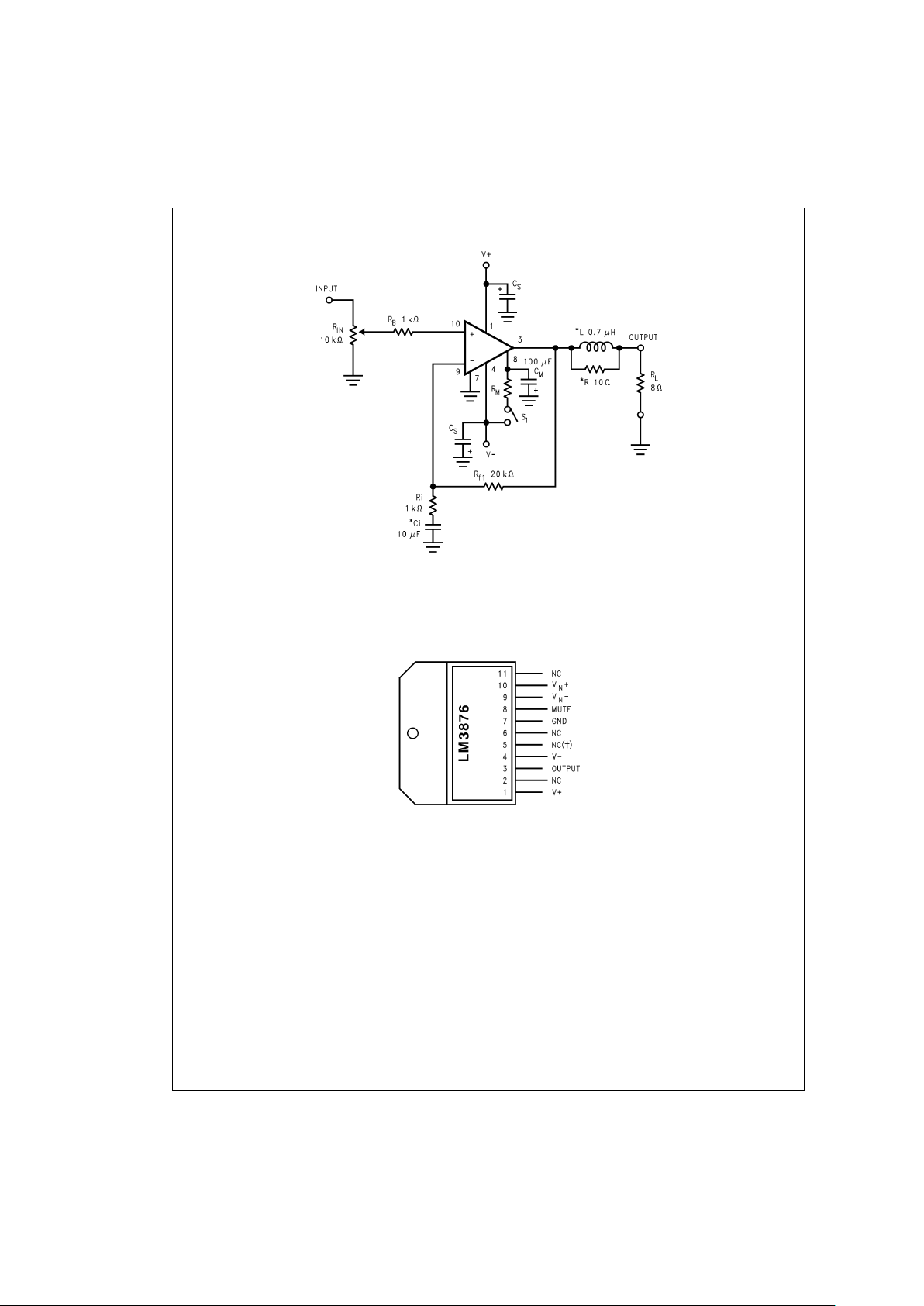
Typical Application
Connection Diagram
DS011832-1
*Optional components dependent upon specific design requirements. Refer to the External Components Description section for a component functional
description.
FIGURE 1. Typical Audio Amplifier Application Circuit
Plastic Package (Note 11)
DS011832-2
†
Connect Pin 5 to V+for Compatibility with LM3886.
Top View
Order Number LM3876T
or LM3876TF
See NS Package Number TA11B for
Staggered Lead Non-Isolated
Package or TF11B for
Staggered Lead Isolated Package
www.national.com 2
Page 3
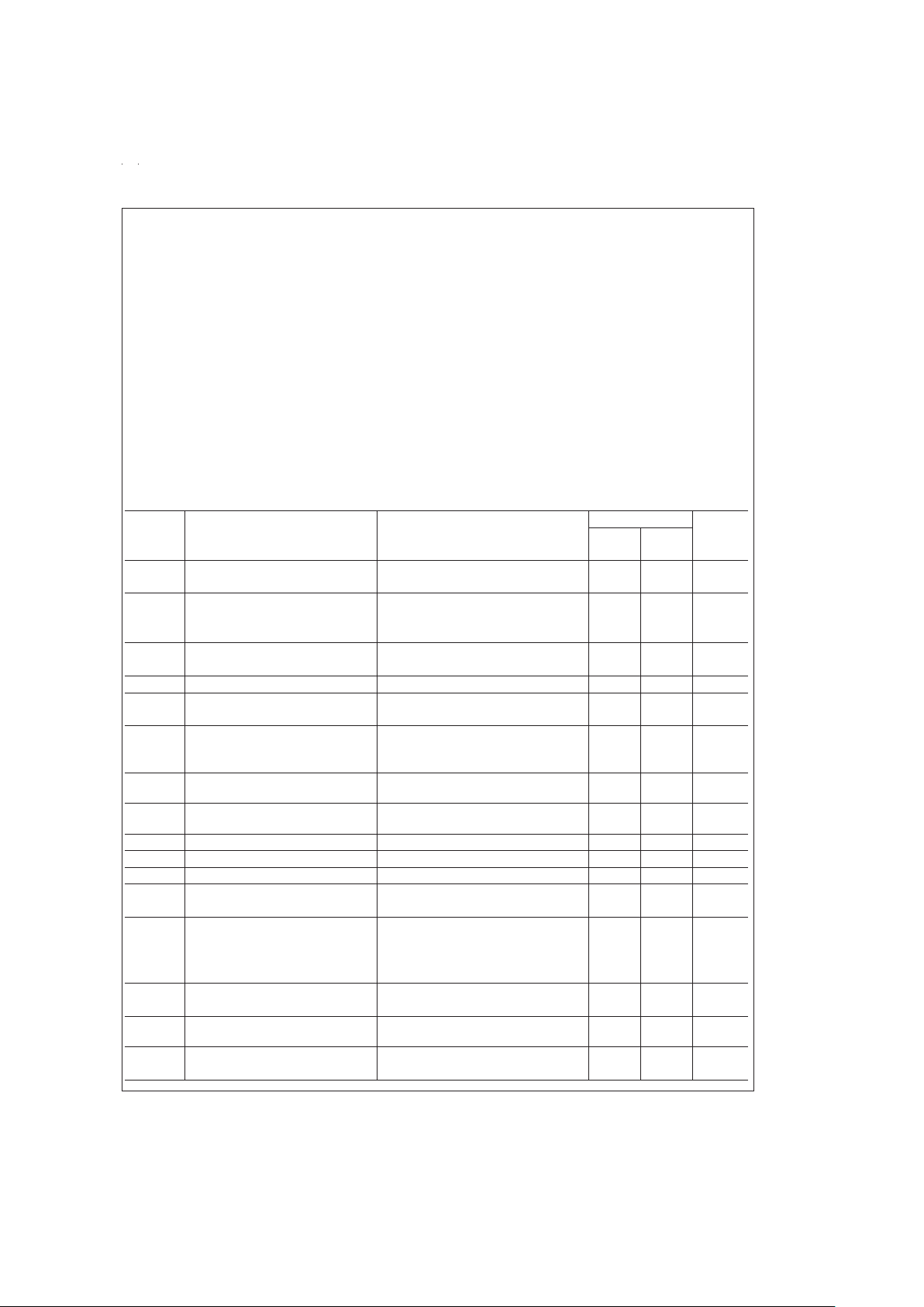
Absolute Maximum Ratings (Notes 4, 5)
If Military/Aerospace specified devices are required,
please contact the National Semiconductor Sales Office/
Distributors for availability and specifications.
Supply Voltage |V
+
|+|V−| (No Signal) 94V
Supply Voltage |V
+
|+|V−| (Input Signal) 84V
Common Mode Input Voltage (V
+
or V−) and
|V
+
|+|V−|≤80V
Differential Input Voltage 60V
Output Current Internally Limited
Power Dissipation (Note 6) 125W
ESD Susceptibility (Note 7) 3000V
Junction Temperature (Note 8) 150˚C
Soldering Information
T Package (10 seconds) 260˚C
Storage Temperature −40˚C to +150˚C
Thermal Resistance
θ
JC
1˚C/W
θ
JA
43˚C/W
Operating Ratings (Notes 4, 5)
Temperature Range
T
MIN
≤ TA≤ T
MAX
−20˚C ≤ TA≤ +85˚C
Supply Voltage |V
+
|+|V−| 24V to 84V
Note 1: Operation is guaranteedup to 84V,however,distortion may beintroduced from SPiKe Protection Circuitry when operating above 70V if proper
thermal considerations are not taken into account. Refer to the Thermal
Considerations section for more information.
(See SPiKe Protection Response)
Electrical Characteristics (Notes 4, 5)
The following specifications apply for V
+
=
+35V, V
−
=
−35V, I
MUTE
=
−0.5 mA with R
L
=
8Ω unless otherwise specified. Limits
apply for T
A
=
25˚C.
Symbol Parameter Conditions LM3876 Units
(Limits)
Typical Limit
(Note 9) (Note 10)
|V
+
|+|V−| Power Supply Voltage (Note 13) V
pin7
−V−≥9V 18 24 V (min)
84 V (max)
A
M
Mute Attenuation Pin 8 Open or at 0V, Mute: On
Current out of Pin 8
>
0.5 mA, 120 80 dB (min)
Mute: Off
P
O
(Note 3)
Output Power (Continuous Average) THD + N=0.1%(max) 56 40 W (min)
f=1 kHz; f=20 kHz
Peak P
O
Instantaneous Peak Output Power 100 W
THD + N Total Harmonic Distortion Plus Noise 40W, 20 Hz ≤ f ≤ 20 kHz 0.06
%
A
V
=
26 dB
SR
(Note 3)
Slew Rate (Note 12) V
IN
=
1.2 Vrms, f=10 kHz,
11 5
V/µs
(min)
Square-Wave, R
L
=
2kΩ
I
+
(Note 2) Total Quiescent Power Supply
Current
V
CM
=
0V, V
o
=
0V, I
o
=
0A, I
mute
=
0A 30 70 mA (max)
V
OS
(Note 2)
Input Offset Voltage V
CM
=
0V, I
o
=
0 mA 1 15 mV (max)
I
B
Input Bias Current V
CM
=
0V, I
o
=
0 mA 0.2 1 µA (max)
I
OS
Input Offset Current V
CM
=
0V, I
o
=
0 mA 0.01 0.2 µA (max)
I
o
Output Current Limit |V+|=|V−|=12V, t
ON
=
10 ms, V
O
=
0V 6 4 A (min)
V
od
(Note 2)
Output Dropout Voltage (Note 14) |V
+
–VO|, V
+
=
20V, I
o
=
+100 mA 1.6 5 V (max)
|V
O
–V−|, V
−
=
−20V, I
o
=
−100 mA 2.7 5 V (max)
PSRR
(Note 2)
Power Supply Rejection Ratio V
+
=
40V to 20V, V
−
=
−40V, 120 85 dB (min)
V
CM
=
0V, I
o
=
0mA
V
+
=
40V, V
−
=
−40V to −20V, 120 85 dB (min)
V
CM
=
0V, I
o
=
0mA
CMRR
(Note 2)
Common Mode Rejection Ratio V
+
=
60V to 20V, V
−
=
−20V to −60V, 120 80 dB (min)
V
CM
=
20V to −20V, I
o
=
0mA
A
VOL
(Note 2)
Open Loop Voltage Gain |V
+
|=|V−|=40V, R
L
=
2kΩ,∆V
O
=
60V 120 90 dB (min)
GBWP Gain-Bandwidth Product |V
+
|=|V−|=40V 8 2 MHz
(min)
f
O
=
100 kHz, V
IN
=
50 mVrms
www.national.com3
Page 4
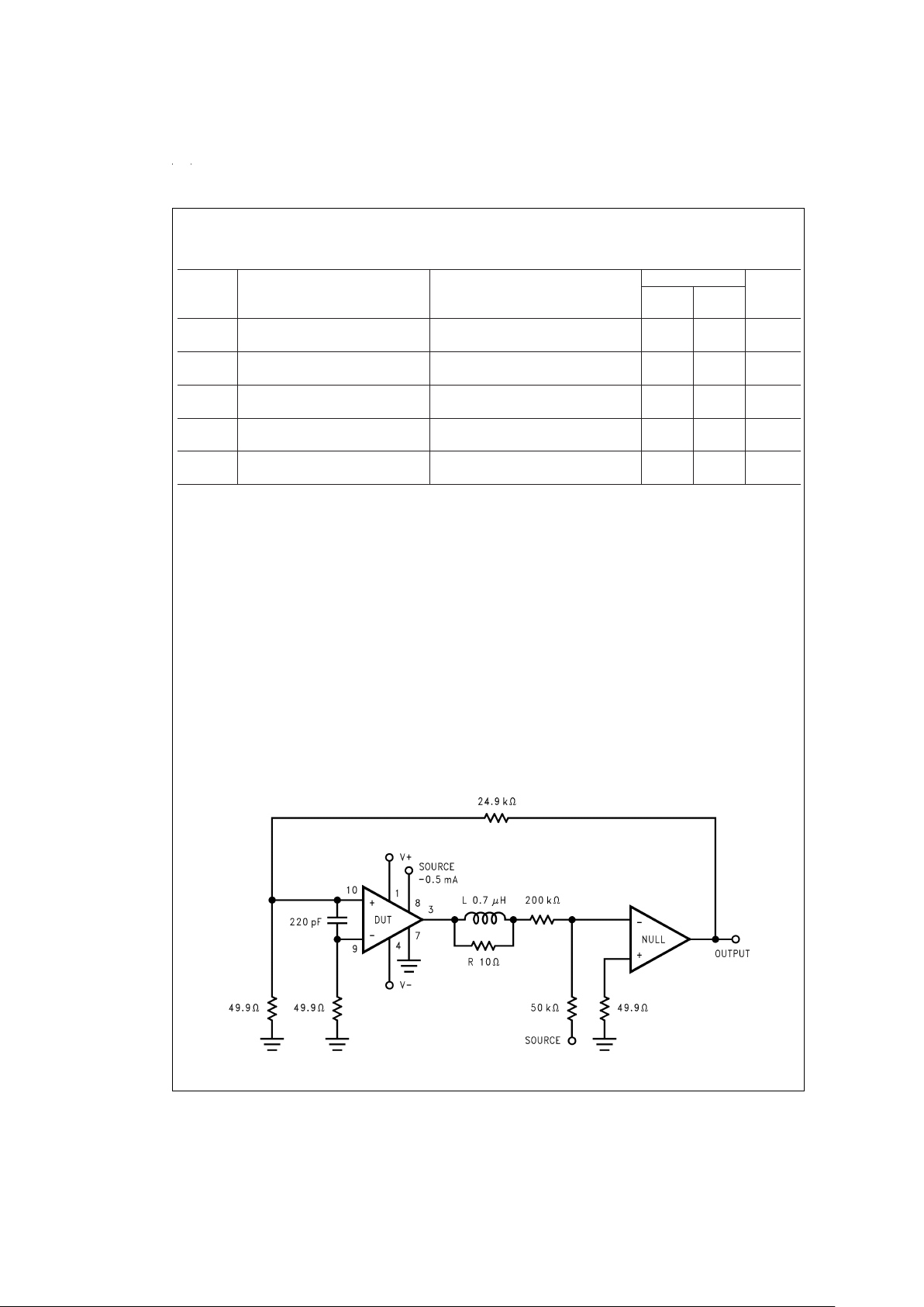
Electrical Characteristics (Notes 4, 5) (Continued)
The following specifications apply for V
+
=
+35V, V
−
=
−35V, I
MUTE
=
−0.5 mA with R
L
=
8Ω unless otherwise specified. Limits
apply for T
A
=
25˚C.
Symbol Parameter Conditions LM3876 Units
(Limits)
Typical Limit
(Note 9) (Note 10)
e
IN
(Note 3)
Input Noise IHF— A Weighting Filter 2.0 8 µV (max)
R
IN
=
600Ω (Input Referred)
SNR Signal-to-Noise Ratio P
O
=
1W, A-Weighted, 98 dB
Measured at 1 kHz, R
S
=
25Ω
P
O
=
40W, A-Weighted, 114 dB
Measured at 1 kHz, R
S
=
25Ω
Ppk=100W, A-Weighted, 122 dB
Measured at 1 kHz, R
S
=
25Ω
IMD Intermodulation Distortion Test 60 Hz, 7 kHz, 4:1 (SMPTE) 0.004
%
60 Hz, 7 kHz, 1:1 (SMPTE) 0.006
Note 2: DC Electrical Test; refer to Test Circuit#1.
Note 3: AC Electrical Test; refer to Test Circuit
#
2.
Note 4: All voltages are measured with respect to the GND pin (pin 7), unless otherwise specified.
Note 5: Absolute Maximum Ratings indicate limits beyond which damage to the device may occur. Operating Ratings indicate conditions for which the device is
functional, but do not guarantee specific performance limits. Electrical Characteristics state DC and AC electrical specifications under particular test conditions which
guarantee specific performance limits. This assumes that the device is within the Operating Ratings. Specifications are not guaranteed for parameters where no limit
is given, however, the typical value is a good indication of device performance.
Note 6: For operating at case temperatures above 25˚C, the device must be derated based on a 150˚C maximum junction temperature and a thermal resistance of
θ
JC
=
1.0 ˚C/W (junction to case). Refer to the Thermal Resistance figure in the Application Information section under Thermal Considerations.
Note 7: Human body model, 100 pF discharged through a 1.5 kΩ resistor.
Note 8: The operating junction temperature maximum is 150˚C, however, the instantaneous Safe Operating Area temperature is 250˚C.
Note 9: Typicals are measured at 25˚C and represent the parametric norm.
Note 10: Limits are guaranteed to National’s AOQL (Average Outgoing Quality Level).
Note 11: The LM3876T package TA11B is a non-isolated package, setting the tab of the device and the heat sink at V
−
potential when the LM3876 is directly
mounted to the heat sink using only thermal compound. If a mica washer is used in addition to thermal compound, θ
CS
(case to sink) is increased, but the heat sink
will be isolated from V
−
.
Note 12: The feedback compensation network limits the bandwidth of the closed-loop response and so the slew rate will be reduced due to the high frequency
roll-off. Without feedback compensation, the slew rate is typically 16V/µs.
Note 13: V
−
must have at least −9V at its pin with reference to ground in order for the under-voltage protection circuitry to be disabled.
Note 14: The output dropout voltage is the supply voltage minus the clipping voltage. Refer to the Clipping Voltage vs Supply Voltage graph in the Typical Performance Characteristics section.
Test Circuit#1 (DC Electrical Test Circuit)
DS011832-3
www.national.com 4
Page 5
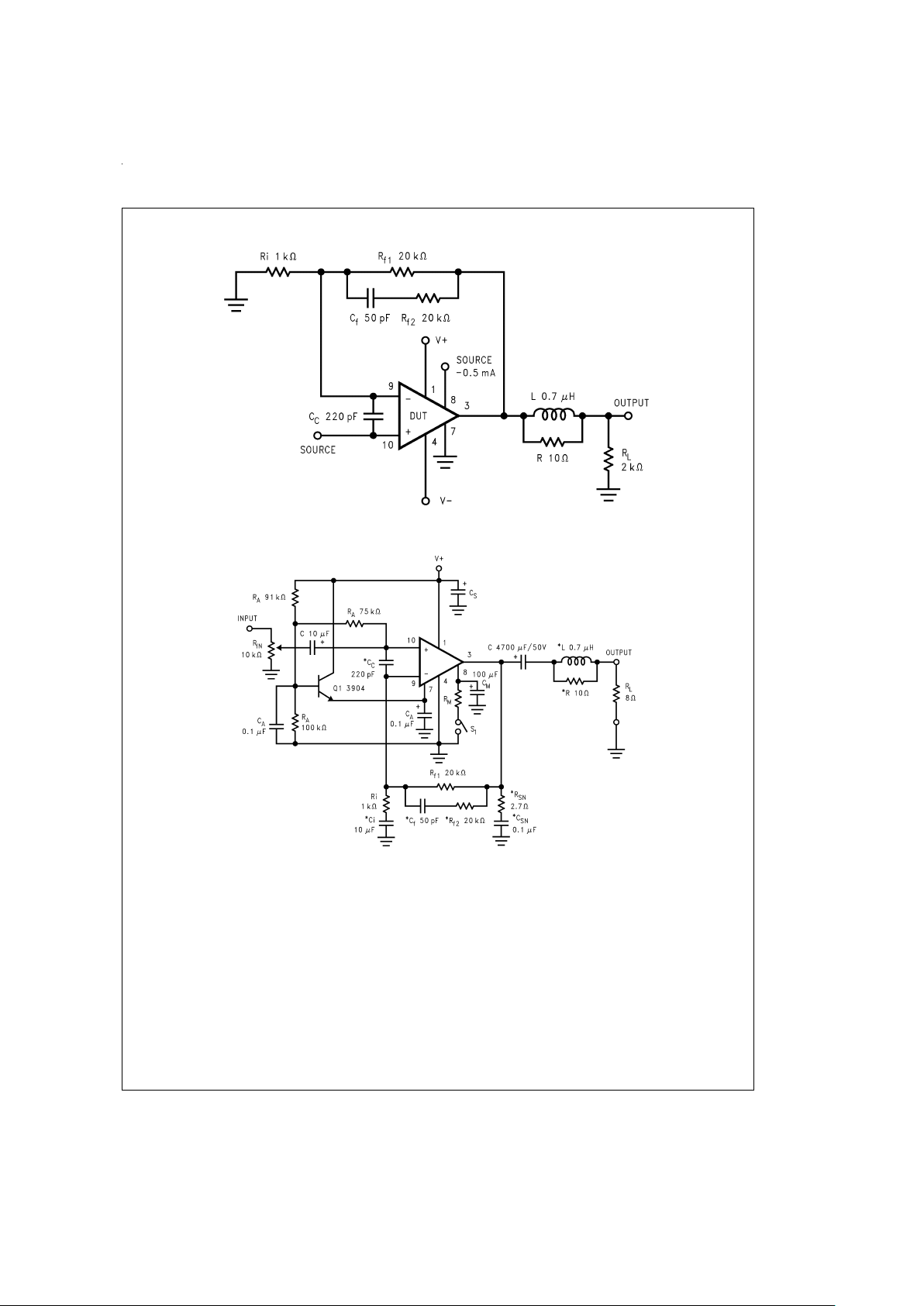
Test Circuit#2 (AC Electrical Test Circuit)
Single Supply Application Circuit
DS011832-4
DS011832-5
*
Optional components dependent upon specific design requirements. Refer to the External
Components Description section for a component functional description.
FIGURE 2. Typical Single Supply Audio Amplifier Application Circuit
www.national.com5
Page 6
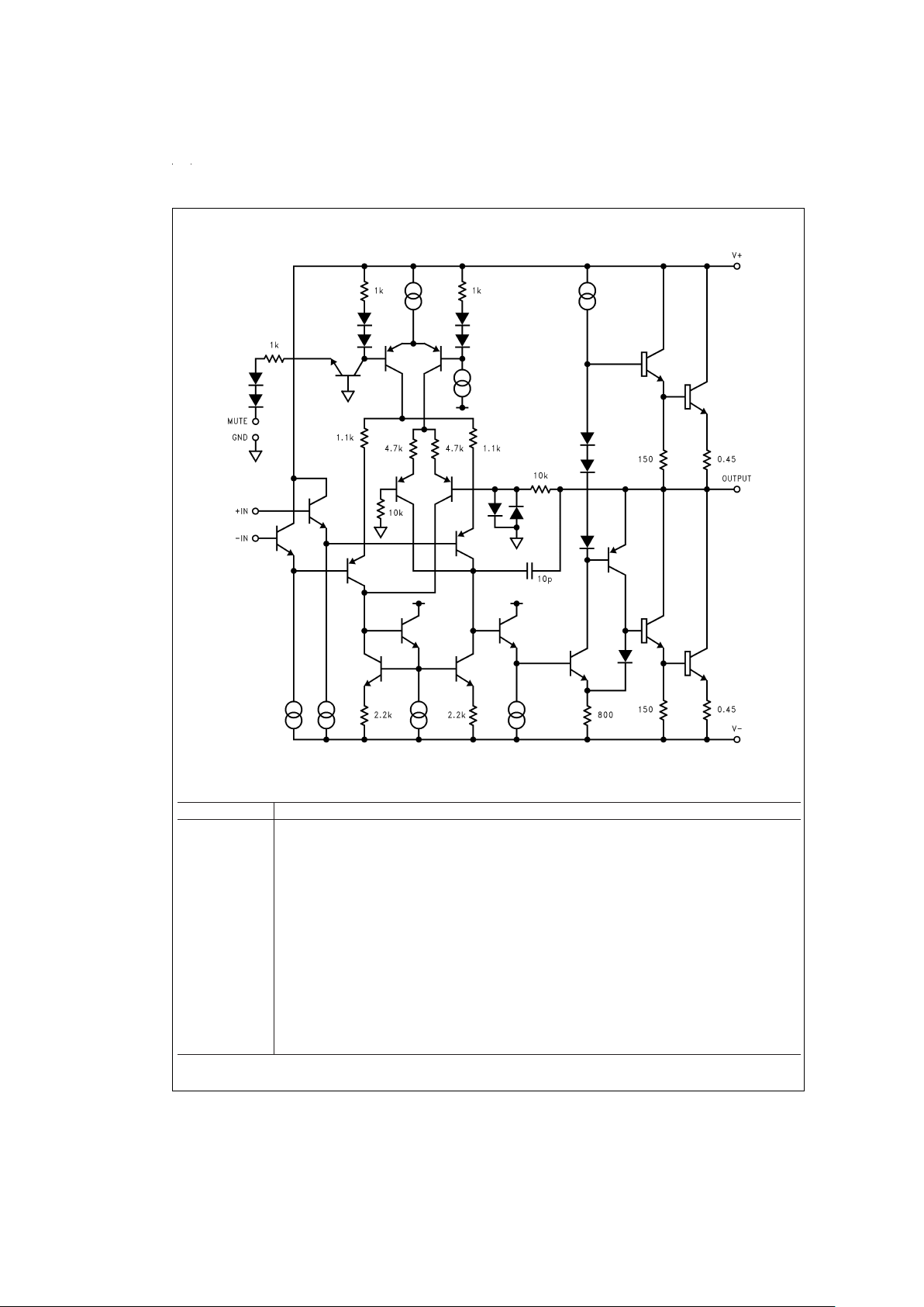
Equivalent Schematic (excluding active protection circuitry)
External Components Description
(
Figures 1, 2
)
Components Functional Description
1. R
IN
Acts as a volume control by setting the voltage level allowed to the amplifier’s input terminals.
2. R
A
Provides DC voltage biasing for the single supply operation and bias current for the positive input terminal.
3. C
A
Provides bias filtering.
4. C Provides AC coupling at the input and output of the amplifier for single supply operation.
5. R
B
Prevents currents from entering the amplifier’s non-inverting input which may be passed through to the load
upon power-down of the system due to the low input impedance of the circuitry when the under-voltage
circuitry is off. This phenomenon occurs when the supply voltages are below 1.5V.
6. C
C
(Note 15)
Reduces the gain (bandwidth of the amplifier) at high frequencies to avoid quasi-saturation oscillations of
the output transistor. The capacitor also suppresses external electromagnetic switching noise created from
fluorescent lamps.
7. Ri Inverting input resistance to provide AC Gain in conjunction with R
f1
.
8. Ci
(Note 15)
Feedback capacitor. Ensures unity gain at DC. Also a low frequency pole (highpass roll-off) at:
f
c
=
1/(2πRi Ci)
9. R
f1
Feedback resistance to provide AC Gain in conjunction with Ri.
DS011832-6
www.national.com 6
Page 7

External Components Description (Continued)
(
Figures 1, 2
)
Components Functional Description
10. R
f2
(Note 15)
At higher frequencies feedback resistance works with C
f
to provide lower AC Gain in conjunction with R
f1
and Ri. A high frequency pole (lowpass roll-off) exists at:
f
c
=
[R
f1Rf2
(s + 1/Rf2Cf)]/[(Rf1+Rf2)(s + 1/Cf(Rf1+Rf2))]
11. C
f
(Note 15)
Compensation capacitor that works with R
f1
and Rf2to reduce the AC Gain at higher frequencies.
12. R
M
Mute resistance set up to allow 0.5 mA to be drawn from pin 8 to turn the muting function off.
→
R
M
is calculated using: RM≤ (|VEE| − 2.6V)/I8 where I8 ≥ 0.5 mA. Refer to the Mute Attenuation vs
Mute Current curves in the Typical Performance Characteristics section.
13. C
M
Mute capacitance set up to create a large time constant for turn-on and turn-off muting.
14. R
SN
(Note 15)
Works with C
SN
to stabilize the output stage by creating a pole that eliminates high frequency oscillations.
15. C
SN
(Note 15)
Works with R
SN
to stabilize the output stage by creating a pole that eliminates high frequency oscillations.
f
c
=
1/(2πR
SNCSN
)
16. L
(Note 15)
Provides high impedance at high frequecies so that R may decouple a highly capacitive load
17. R
(Note 15)
and reduce the Q of the series resonant circuit due to capacitive load. Also provides a low impedance at
low frequencies to short out R and pass audio signals to the load.
18. C
S
Provides power supply filtering and bypassing.
19. S1 Mute switch that mutes the music going into the amplifier when opened.
Note 15: Optional components dependent upon specific design requirements. Refer to the Application Information section for more information.
OPTIONAL EXTERNAL COMPONENT INTERACTION
Although the optional external components have specific desired functions that are designed to reduce the bandwidth and eliminate unwanted high frequency oscillations they may cause certain undesirable effects when they interact. Interaction may occur
for components whose reactances are in close proximity to one another. One example would be the coupling capacitor, C
C
, and
the compensation capacitor, Cf. These two components act as low impedances to certain frequencies which will couple signals
from the input to the output. Please take careful note of basic amplifier component functionality when designing in these components.
The optional external components shown in
Figure 2
and described above are applicable in both single and split voltage supply
configurations.
Typical Performance Characteristics
Safe Area
DS011832-17
SPiKe
Protection Response
DS011832-18
Supply Current vs
Supply Voltage
DS011832-19
www.national.com7
Page 8

Typical Performance Characteristics (Continued)
Pulse Thermal
Resistance
DS011832-20
Pulse Thermal
Resistance
DS011832-21
Supply Current vs
Output Voltage
DS011832-22
Pulse Power Limit
DS011832-23
Pulse Power Limit
DS011832-24
Supply Current vs
Case Temperature
DS011832-25
Pulse Response
DS011832-26
Input Bias Current vs
Case Temperature
DS011832-27
Clipping Voltage vs
Supply Voltage
DS011832-28
www.national.com 8
Page 9

Typical Performance Characteristics (Continued)
THD+N vs Frequency
DS011832-29
THD+N vs Output Power
DS011832-30
THD+N vs Output Power
DS011832-31
THD+N Distribution
DS011832-32
THD+N Distribution
DS011832-33
Output Power vs
Load Resistance
DS011832-34
Max Heatsink Thermal Resistance (˚C/W)
at the Specified Ambient Temperature (˚C)
PDmax
r vs Supply Voltage
DS011832-9
Note: The maximum heat sink thermal resistance values, øSA, in the table above were calculated using a øCS= 0.2˚C/W due to thermal compound
www.national.com9
Page 10

Typical Performance Characteristics (Continued)
Power Dissipation vs
Output Power
DS011832-35
Power Dissipation vs
Output Power
DS011832-36
Output Power vs
Supply Voltage
DS011832-37
IMD 60 Hz, 4:1
DS011832-38
IMD 60 Hz, 7 kHz, 4:1
DS011832-39
IMD 60 Hz, 7 kHz, 4:1
DS011832-40
IMD 60 Hz, 1:1
DS011832-41
IMD 60 Hz, 7 kHz 1:1
DS011832-42
IMD 60 Hz, 7 kHz, 1:1
DS011832-43
www.national.com 10
Page 11

Typical Performance Characteristics (Continued)
Application Information
GENERAL FEATURES
Mute Function: The muting function of the LM3876 allows
the user to mute the music going into the amplifier by drawing less than 0.5 mAout of pin 8 of the device. This is accomplished as shown in the Typical Application Circuit where the
resistor R
M
is chosen with reference to your negative supply
voltage and is used in conjuction with a switch. The switch
(when opened) cuts off the current flow from pin 8 to V
−
, thus
placing the LM3876 into mute mode. Refer to the Mute Attenuation vs Mute Current curves in the Typical Perfor-
mance Characteristics section for values of attenuation per
current out of pin 8. The resistance R
M
is calculated by the
following equation:
R
M
(|VEE| − 2.6V)/I8 where I8 ≥ 0.5 mA.
Under-Voltage Protection: Upon system power-up the
under-voltage protection circuitry allows the power supplies
and their corresponding caps to come up close to their full
values before turning on the LM3876 such that no DC output
spikes occur. Upon turn-off, the output of the LM3876 is
brought to ground before the power supplies such that no
transients occur at power-down.
Over-Voltage Protection: The LM3876 contains overvoltage protection circuitry that limits the output current to approximately 6Apeak while also providing voltage clamping,
though not through internal clamping diodes. The clamping
effect is quite the same, however, the output transistors are
designed to work alternately by sinking large current spikes.
SPiKe Protection: The LM3876 is protected from instantaneous peak-temperature stressing by the power transistor
array.The Safe Operating Area graph in the Typical Perfor-
mance Characteristics section shows the area of device
operation where the SPiKe Protection Circuitry is not enabled. The waveform to the right of the SOA graph exemplifies how the dynamic protection will cause waveform distortion when enabled.
Thermal Protection: The LM3876 has a sophisticated thermal protection scheme to prevent long-term thermal stress
to the device. When the temperature on the die reaches
165˚C, the LM3876 shuts down. It starts operating again
when the die temperature drops to about 155˚C, but if the
temperature again begins to rise, shutdown will occur again
at 165˚C. Therefore the device is allowed to heat up to a
relatively high temperature if the fault condition is temporary,
but a sustained fault will cause the device to cycle in a
Schmitt Trigger fashion between the thermal shutdown temperature limits of 165˚C and 155˚C. This greatly reduces the
stress imposed on the IC by thermal cycling, which in turn
improves its reliability under sustained fault conditions.
Since the die temperature is directly dependent upon the
heat sink, the heat sink should be chosen as discussed in
the Thermal Considerations section, such that thermal
shutdown will not be reached during normal operation. Using
the best heat sink possible within the cost and space constraints of the system will improve the long-term reliability of
any power semiconductor device.
Mute Attenuation vs
Mute Current
DS011832-44
Mute Attenuation vs
Mute Current
DS011832-45
Large Signal Response
DS011832-46
Power Supply
Rejection Ratio
DS011832-47
Common-Mode
Rejection Ratio
DS011832-48
Open Loop
Frequency Response
DS011832-49
www.national.com11
Page 12

Application Information (Continued)
THERMAL CONSIDERATIONS
Heat Sinking
The choice of a heat sink for a high-power audio amplifier is
made entirely to keep the die temperature at a level such
that the thermal protection circuitry does not operate under
normal circumstances. The heat sink should be chosen to
dissipate the maximum IC power for a given supply voltage
and rated load.
With high-power pulses of longer duration than 100 ms, the
case temperature will heat up drastically without the use of a
heat sink. Therefore the case temperature, as measured at
the center of the package bottom, is entirely dependent on
heat sink design and the mounting of the IC to the heat sink.
For the design of a heat sink for your audio amplifier application refer to the Determining The Correct Heat Sink section.
Since a semiconductor manufacturer has no control over
which heat sink is used in a particular amplifier design, we
can only inform the system designer of the parameters and
the method needed in the determination of a heat sink. With
this in mind, the system designer must choose his supply
voltages, a rated load, a desired output power level, and
know the ambient temperature surrounding the device.
These parameters are in addition to knowing the maximum
junction temperature and the thermal resistance of the IC,
both of which are provided by National Semiconductor.
As a benefit to the system designer we have provided Maximum Power Dissipation vs Supply Voltages curves for various loads in the Typical Performance Characteristics section, giving an accurate figure for the maximum thermal
resistance required for a particular amplifier design. This
data wasbased on θ
JC
=
1˚C/W andθ
CS
=
0.2˚C/W.We also
provide a section regarding heat sink determination for any
audio amplifier design where θ
CS
may be a different value. It
should be noted that the idea behind dissipating the maximum power within the IC is to provide the device with a low
resistance to convection heat transfer such as a heat sink.
Therefore, it is necessary for the system designer to be conservative in his heat sink calculations. As a rule, the lower
the thermal resistance of the heat sink the higher the amount
of power that may be dissipated. This is of course guided by
the cost and size requirements of the system. Convection
cooling heat sinks are available commercially, and their
manufacturers should be consulted for ratings.
Proper mounting of the IC is required to minimize the thermal
drop between the package and the heat sink. The heat sink
must also have enough metal under the package to conduct
heat from the center of the package bottom to the fins without excessive temperature drop.
A thermal grease such as Wakefield type 120 or Thermalloy
Thermacote should be used when mounting the package to
the heat sink. Without this compound, thermal resistance will
be no better than 0.5˚C/W, and probably much worse. With
the compound, thermal resistance will be 0.2˚C/W or less,
assuming under 0.005 inch combined flatness runout for the
package and heat sink. Proper torquing of the mounting
bolts is important and can be determined from heat sink
manufacturer’s specification sheets.
Should it be necessary to isolate V
−
from the heat sink, an insulating washer is required. Hard washers like beryluum oxide, anodized aluminum and mica require the use of thermal
compound on both faces. Two-mil mica washers are most
common, giving about 0.4˚C/W interface resistance with the
compound.
Silicone-rubber washers are also available. A 0.5˚C/W thermal resistance is claimed without thermal compound. Experience has shown that these rubber washers deteriorate and
must be replaced should the IC be dismounted.
Determining Maximum Power Dissipation
Power dissipation within the integrated circuit package is a
very important parameter requiring a thorough understanding if optimum power output is to be obtained. An incorrect
maximum power dissipation (P
D
) calculation may result in inadequate heat sinking, causing thermal shutdown circuitry to
operate and limit the output power.
The followingequations can be used to acccurately calculate
the maximum and average integrated circuit power dissipation for your amplifier design, given the supply voltage, rated
load, and output power. These equations can be directly applied to the Power Dissipation vs Output Power curves in the
Typical Performance Characteristics section.
Equation (1)
exemplifies the maximum power dissipation of
the ICand
Equations (2), (3)
exemplify theaverage IC power
dissipation expressed in different forms.
P
DMAX
=
V
CC
2/2π2R
L
(1)
where V
CC
is the total supply voltage
P
DAVE
=
(V
Opk/RL
)[VCC/π −V
Opk
/2] (2)
where V
CC
is the total supply voltage and V
Opk
=
V
CC
/π
P
DAVE
=
V
CCVOpk
/πRL−V
Opk
2
/2R
L
(3)
where V
CC
is the total supply voltage.
Determining the Correct Heat Sink
Once the maximum IC power dissipation is known for a
given supply voltage, rated load, and the desired rated output power the maximum thermal resistance (in ˚C/W) of a
heat sink can be calculated. This calculation is made using
Equation (4)
and is based on the fact that thermal heat flow
parameters are analogous to electrical current flow properties.
It is also known that typically the thermal resistance, θ
JC
(junction to case), of the LM3876 is 1˚C/W and that using
Thermalloy Thermacote thermal compound provides a thermal resistance, θ
CS
(case to heat sink), of about 0.2˚C/W as
explained in the Heat Sinking section.
Referring to the figure below,it is seen that the thermal resis-
tance from the die (junction) to the outside air (ambient) is a
combination of three thermal resistances, two of which are
known, θ
JC
and θCS. Since convection heat flow (power dissipation) is analogous to current flow, thermal resistance is
analogous to electrical resistance, and temperature drops
are analogous to voltage drops, the power dissipation out of
the LM3876 is equal to the following:
P
DMAX
=
(T
Jmax−TAmb
)/θ
JA
where θ
JA
=
θ
JC
+ θCS+ θ
SA
DS011832-12
www.national.com 12
Page 13

Application Information (Continued)
But since we know P
DMAX
, θJC, and θSCfor the application
and we are looking for θ
SA
, we have the following:
θ
SA
=
[(T
Jmax−TAmb
)−P
DMAX(θJC
+ θCS)]/P
DMAX
(4)
Again it must be noted that the value of θ
SA
is dependent
upon the system designer’s amplifier application and its corresponding parameters as described previously. If the ambient temperature that the audio amplifier is to be working under is higher than the normal 25˚C, then the thermal
resistance for the heat sink, given all other things are equal,
will need to be smaller.
Equations (1), (4)
are the only equations needed in the determination of the maximum heat sink thermal resistance.
This is of course given that the system designer knows the
required supply voltages to drive his rated load at a particular
power output level and the parameters provided by the semiconductor manufacturer. These parameters are the junction
to case thermal resistance, θ
JC,TJmax
=
150˚C, and the recommended Thermalloy Thermacote thermal compound resistance, θ
CS
.
SIGNAL-TO-NOISE RATIO
In the measurement of the signal-to-noise ratio, misinterpretations of the numbers actually measured are common. One
amplifier may sound much quieter than another, but due to
improper testing techniques, they appear equal in measurements. This is often the case when comparing integrated circuit designs to discrete amplifier designs. Discrete transistor
amps often “run out of gain” at high frequencies and therefore have small bandwidths to noise as indicated below.
Integrated circuits have additional open loop gain allowing
additional feedback loop gain in order to lower harmonic distortion and improve frequency response. It is this additional
bandwidth that can lead to erroneous signal-to-noise measurements if not considered during the measurement process. In the typical example above, the difference in bandwidth appears small on a log scale but the factor of 10 in
bandwidth, (200kHz to 2 MHz) can result in a 10 dB theoretical difference in the signal-to-noise ratio (white noise is proportional to the square root of the bandwidth in a system).
In comparing audio amplifiers it is necessary to measure the
magnitude of noise in the audible bandwidth by using a
“weighting” filter (Note 16). A “weighting” filter alters the frequency response in order to compensate for the average human ear’s sensitivity to the frequency spectra. The weighting
filters at the same time provide the bandwidth limiting as discussed in the previous paragraph.
Note 16: CCIR/ARM:
A Practical Noise Measurement Method;
by Ray
Dolby, David Robinson and Kenneth Gundry, AES Preprint No. 1353 (F-3).
In addition to noise filtering, differing meter types give different noise readings. Meter responses include:
1. RMS reading,
2. average responding,
3. peak reading, and
4. quasi peak reading.
Although theoretical noise analysis is derived using true
RMS based calculations, most actual measurements are
taken with ARM (Average Responding Meter) test equipment.
Typicalsignal-to-noise figures are listed for anA-weighted filter which is commonly used in the measurement of noise.
The shape of all weighting filters is similar, with the peak of
the curve usually occurring in the 3 kHz–7 kHz region as
shown below.
SUPPLY BYPASSING
The LM3876 has excellent power supply rejection and does
not require a regulated supply. However, to eliminate possible oscillations all op amps and power op amps should
have their supply leads bypassed with low-inductance capacitors having short leads and located close to the package
terminals. Inadequate power supply bypassing will manifest
itself by a low frequency oscillation known as “motorboating”
or by high frequency instabilities. These instabilities can be
eliminated through multiple bypassing utilizing a large tantalum orelectrolytic capacitor (10 µF or larger) which is used to
absorb low frequency variations and a small ceramic capacitor (0.1 µF) to prevent any high frequency feedback through
the power supply lines.
If adequate bypassing is not provided the current in the supply leads which is a rectified component of the load current
may befed back into internal circuitry.This signal causes low
distortion at high frequencies requiring that the supplies be
bypassed at the package terminals with an electrolytic capacitor of 470 µF or more.
LEAD INDUCTANCE
Power op amps are sensitive to inductance in the output
lead, particularly with heavy capacitive loading. Feedback to
the input should be taken directly from the output terminal,
minimizing common inductance with the load.
Lead inductance can also cause voltage surges on the supplies. With long leads to the power supply,energy is stored in
the lead inductance when the output is shorted. This energy
can be dumped back into the supply bypass capacitorswhen
the short is removed. The magnitude of this transient is reduced by increasing the size of the bypass capacitor near
the IC. With at least a 20 µF local bypass, these voltage
surges areimportant only if thelead length exceeds a couple
feet (
>
1 µH lead inductance). Twisting together the supply
and ground leads minimizes the effect.
DS011832-13
DS011832-14
www.national.com13
Page 14

Application Information (Continued)
LAYOUT, GROUND LOOPS AND STABILITY
The LM3876 is designed to be stable when operated at a
closed-loop gain of 10 or greater, but as with any other
high-current amplifier, the LM3876 can be made to oscillate
under certain conditions. These usually involve printed circuit board layout or output/input coupling.
When designing a layout, it is important to return the load
ground, the output compensation ground, and the low level
(feedback and input) grounds to the circuit board common
ground point through separate paths. Otherwise, large currents flowing along a ground conductor will generate voltages on the conductor which can effectively act as signals at
the input, resulting in high frequency oscillation or excessive
distortion. It is advisable to keep the output compensation
components and the 0.1 µF supply decoupling capacitors as
close as possible to the LM3876 to reduce the effects of PCB
trace resistance and inductance. For the same reason, the
ground return paths should be as short as possible.
In general, with fast, high-current circuitry, all sorts of problems can arise from improper grounding which again can be
avoided by returning all grounds separately to a common
point. Without isolating the ground signals and returning the
grounds to a common point, ground loops may occur.
“Ground Loop” is the term used to describe situations occurring in ground systems where a difference in potential exists
between two ground points. Ideally a ground is a ground, but
unfortunately, in order for this to be true, ground conductors
with zero resistance are necessary. Since real world ground
leads possess finite resistance, currents running through
them will cause finite voltage drops to exist. If two ground return lines tie into the same path at different points there will
be a voltage drop between them. The first figure below
shows a common ground example where the positive input
ground and the load ground are returned to the supply
ground point via the same wire. The addition of the finite wire
resistance, R
2
, results in a voltage difference between the
two points as shown below.
The load current I
L
will be much larger than input bias current
I
I
, thus V1will follow the output voltage directly,i.e. in phase.
Therefore the voltage appearing at the non-inverting input is
effectively positive feedback and the circuit may oscillate. If
there were only one device to worry about then the values of
R
1
and R2would probably be small enough to be ignored;
however, several devices normally comprise a total system.
Any ground return of a separate device, whose output is in
phase, can feedback in a similar manner and cause instabilities. Out of phase ground loops also are troublesome, causing unexpected gain and phase errors.
The solution to most ground loop problems is to always use
a single-point ground system, although this is sometimes impractical. The third figure below is an example of a
single-point ground system.
The single-point ground concept should be applied rigorously to all components and all circuits when possible. Violations of single-point grounding are most common among
printed circuit board designs, since the circuit is surrounded
by large ground areas which invite the temptation to run a
device to the closest ground spot. As a final rule, make all
ground returns low resistance and low inductance by using
large wire and wide traces.
Occasionally, current in the output leads (which function as
antennas) can be coupled through the air to the amplifier input, resulting in high-frequency oscillation. This normally
happens when the source impedance is high or the input
leads are long. The problem can be eliminated by placing a
small capacitor,C
C
, (on the order of 50 pF to 500 pF) across
the LM3876 input terminals. Refer to the External Compo-
nents Description section relating to component interaction
with C
f
.
REACTIVE LOADING
It is hard for most power amplifiers to drive highly capacitive
loads very effectively and normally results in oscillations or
ringing on the square wave response. If the output of the
LM3876 is connected directly to a capacitor with no series
resistance, the square wave response will exhibit ringing if
the capacitanceis greater than about0.2 µF.If highly capacitive loads are expected due to long speaker cables, a
method commonly employed to protect amplifiers from low
impedances at high frequencies is to couple to the load
through a 10Ω resistor in parallel with a 0.7 µH inductor.The
inductor-resistor combination as shown in the Typical Appli-
cation Circuit isolates the feedback amplifier from the load
by providing high output impedance at high frequencies thus
allowing the10Ω resistor to decouple the capacitive load and
reduce the Q of the series resonant circuit. The LR combination also provides low output impedance at low frequencies
thus shorting out the 10Ω resistor and allowing the amplifier
to drive the series RC load (large capacitive load due to long
speaker cables) directly.
GENERALIZED AUDIO POWER AMPLIFIER DESIGN
The system designer usually knows some of the following
parameters when starting an audio amplifier design:
Desired Power Output Input Level
Input Impedance Load Impedance
Maximum Supply Voltage Bandwidth
The power output and load impedance determine the power
supply requirements, however, depending upon the application some system designers may be limited to certain maximum supply voltages. If the designer does have a power
supply limitation, he should choose a practical load imped-
DS011832-15
www.national.com 14
Page 15

Application Information (Continued)
ance which would allow the amplifier to provide the desired
output power, keeping in mind the current limiting capabilities of the device. In any case, the output signal swing and
current are found from (where P
O
is the average output
power):
(5)
(6)
To determine the maximum supply voltage the following parameters must be considered. Add the dropout voltage (5V
for LM3876) to the peak output swing, V
opeak
, to get the sup-
ply rail value (i.e.
±
(V
opeak
+ Vod)at a current of I
opeak
). The
regulation of the supply determines the unloaded voltage,
usually about 15%higher. Supply voltage will also rise 10
%
during high line conditions. Therefore, the maximum supply
voltage is obtained from the following equation:
Max. supplies ≈
±
(V
opeak
+ Vod)(1 + regulation)(1.1)(7)
The input sensitivity and the output power specs determine
the minimum required gain as depicted below:
(8)
Normally the gain is set between 20 and 200; for a 40W, 8Ω
audio amplifier this results in a sensitivity of 894 mV and
89 mV, respectively.Although higher gain amplifiers provide
greater output power and dynamic headroom capabilities,
there are certain shortcomings that go along with the so
called “gain.” The input referred noise floor is increased and
hence the SNR is worse. With the increase in gain, there is
also a reduction of the power bandwidth which results in a
decrease in feedback thus not allowing the amplifier to respond quickly enough to nonlinearities. This decreased ability to respond to nonlinearities increases the THD + N specification.
The desired input impedance is set by R
IN
. Very high values
can cause board layout problems and DC offsets at the output. The value for the feedback resistance, R
f1
, should be
chosen to be a relatively large value (10 kΩ–100 kΩ), and
the other feedback resistance, Ri, is calculated using standard op amp configuration gain equations. Most audio amplifiers are designed from the non-inverting amplifier configuration.
DESIGN A 40W/8Ω AUDIO AMPLIFIER
Given:
Power Output 40W
Load Impedance 8Ω
Input Level 1V(max)
Input Impedance 100 kΩ
Bandwidth 20 Hz–20 kHz
±
0.25 dB
Equations (5), (6)
give:
40W/8Ω V
opeak
=
25.3V I
opeak
=
3.16A
Therefore the supply required is:
±
With 15%regulation and high line the final supply voltage is
±
38.3V using
Equation (7)
. At this point it is a good idea to
check thePower Output vs SupplyVoltage to ensure that the
required output power is obtainable from the device while
maintaining low THD + N. It is also good to check the Power
Dissipation vs Supply Voltage to ensure that the device can
handle the internal power dissipation. At the same time designing in a relatively practical sized heat sink with a low
thermal resistance is also important. Refer to Typical Per-
formance Characteristics graphs and the Thermal Considerations section for more information.
The minimum gain from
Equation (8)
is: AV≥ 18
We select a gain of 21 (Non-Inverting Amplifier); resulting in
a sensitivity of 894 mV.
Letting R
IN
equal 100 kΩ gives the required input impedance, however, this would eliminate the “volume control” unless an additional input impedance was placed in series with
the 10 kΩ potentiometer that is depicted in
Figure 1
. Adding
the additional 100 kΩ resistor would ensure the minumum
required input impedance.
For low DC offsets at the output we let R
f1
=
100 kΩ. Solving
for Ri (Non-Inverting Amplifier) gives the following:
Ri=R
f1
/(AV−1)=100k/(21 − 1)=5kΩ; use 5.1 kΩ
The bandwidth requirement must be stated as a pole, i.e.,
the 3 dB frequency. Five times away from a pole gives
0.17 dB down, which is better than the required 0.25 dB.
Therefore:
f
L
=
20 Hz/5=4Hz
f
H
=
20 kHz x 5=100 kHz
At this point, it is a good idea to ensure that the
Gain-Bandwidth Product for the part will provide the designed gain out to the upper 3 dB point of 100 kHz. This is
why the minimum GBWP of the LM3876 is important.
GBWP ≥ A
V
xf3dB=21 x 100 kHz=2.1 MHz
GBWP=2.0 MHz (min) for the LM3876
Solving for the low frequency roll-off capacitor, Ci, we have:
Ci ≥ 1/(2π Ri f
L
)=7.8 µF; use 10 µF.
Definition of Terms
Input Offset Voltage: The absolute value of the voltage
which must be applied between the input terminals through
two equal resistances to obtain zero output voltage and current.
Input Bias Current: The absolute value of the average of
the two input currents with the output voltage and current at
zero.
Input Offset Current: The absolute value of the difference
in the two input currents with the output voltage and current
at zero.
Input Common-Mode Voltage Range (or Input Voltage
Range): The range of voltages on the input terminals for
which the amplifier is operational. Note that the specifications are not guaranteed over the full common-mode voltage
range unless specifically stated.
Common-Mode Rejection: The ratio of the input
common-mode voltage range to the peak-to-peak change in
input offset voltage over this range.
Power Supply Rejection: The ratio of the change in input
offset voltage to the change in power supply voltages producing it.
Quiescent Supply Current: The current required from the
power supply to operate the amplifier with no load and the
output voltage and current at zero.
Slew Rate: The internally limited rate of change in output
voltage with a large amplitude step function applied to the input.
www.national.com15
Page 16

Definition of Terms (Continued)
Class B Amplifier: The most common type of audio power
amplifier that consists of two output devices each of which
conducts for 180˚ of the input cycle. The LM3876 is a
Quasi-AB type amplifier.
Crossover Distortion: Distortion caused in the output stage
of a class B amplifier. It can result from inadequate bias current providing a dead zone where the output does not respond to the input as the input cycle goes through its zero
crossing point. Also for ICs an inadequate frequency response of the output PNP device can cause a turn-on delay
giving crossover distortion on the negative going transition
through zero crossing at the higher audio frequencies.
THD+N:Total Harmonic Distortion plus Noise refers to the
measurement technique in which the fundamental component is removed by a bandreject (notch) filter and all remaining energy is measured including harmonics and noise.
Signal-to-Noise Ratio: The ratio of a system’s output signal
level to the system’s output noise level obtained in the absence of a signal. The output reference signal is either specified or measured at a specified distortion level.
Continuous Average Output Power: The minimum sine
wave continuous average power output in watts (or dBW)
that can be delivered into the rated load, over the rated
bandwidth, at the rated maximum total harmonic distortion.
Music Power: Ameasurement of the peak output power capability of an amplifier with either a signal duration sufficiently short that the amplifier power supply does not sag
during the measurement, or when high quality external
power supplies are used. This measurement (an IHF standard) assumes that with normal music program material the
amplifier power supplies will sag insignificantly.
Peak Power: Most commonly referred to as the power output capability of an amplifier that can be delivered to the
load; specified by the part’s maximum voltage swing.
Headroom: The margin between an actual signal operating
level (usually the power rating of the amplifier with particular
supply voltages, a rated load value, and a rated THD + N figure) and the level just before clipping distortion occurs, expressed in decibels.
Large Signal Voltage Gain: The ratio of the output voltage
swing to the differential input voltage required to drive the
output from zero to either swing limit. The output swing limit
is the supply voltage less a specified quasi-saturation voltage.A pulse of short enough duration to minimize thermal effects is used as a measurement signal.
Output-Current Limit: The output current with a fixed output voltage and a large input overdrive. The limiting current
drops with time once SPiKe protection circuitry is activated.
Output Saturation Threshold (Clipping Point): The output
swing limit for a specified input drive beyond that required for
zero output. It is measured with respect to the supply to
which the output is swinging.
Output Resistance: The ratio of the change in output voltage to the change in output current with the output around
zero.
Power Dissipation Rating: The power that can be dissipated for a specified time interval without activating the protection circuitry. For time intervals in excess of 100 ms, dissipation capability is determined by heat sinking of the IC
package rather than by the IC itself.
Thermal Resistance: The peak, junction-temperature rise,
per unit of internal power dissipation (units in ˚C/W), above
the case temperature as measured at the center of the package bottom.
The DC thermal resistance applies when one output transistor is operating continuously. The AC thermal resistance applies with the output transistors conducting alternately at a
high enough frequency that the peak capability of neither
transistor is exceeded.
Power Bandwidth: The power bandwidth of an audio amplifier is the frequency range over which the amplifier voltage
gain does not fall below 0.707 of the flat band voltage gain
specified for a given load and output power.
Power bandwidth also can be measured by the frequencies
at which a specified level of distortion is obtained while the
amplifier delivers a power output 3 dB below the rated output. For example, an amplifier rated at 60W with ≤ 0.25
%
THD + N, would make its power bandwidth measured as the
difference between the upper and lower frequencies atwhich
0.25%distortion was obtained while the amplifier was delivering 30W.
Gain-Bandwidth Product: The Gain-Bandwidth Product is
a way of predicting the high-frequency usefulness of an op
amp. The Gain-Bandwidth Product is sometimes called the
unity-gain frequency or unity-gain cross frequency because
the open-loop gain characteristic passes through or crosses
unity gain at this frequency.Simply, we have the following relationship: A
CL1xf1
=
A
CL2xf2
Assuming that at unity-gain (A
CL1
=
1 or (0 dB)) fu=fi
=
GBWP, then we have the following: GBWP=A
CL2
xf2
This says that once fu (GBWP) is known for an amplifier,
then the open-loop gain can be found at any frequency. This
is also an excellent equation to determine the 3 dB point of a
closed-loop gain, assuming that you know the GBWP of the
device. Refer to the diagram on the following page.
Biamplification: The technique of splitting the audio frequency spectrum into two sections and using individual
power amplifiers to drive a separate woofer and tweeter.
Crossover frequencies for the amplifiers usually vary between 500 Hz and 1600 Hz. “Biamping” has the advantages
of allowing smaller power amps to produce a given sound
pressure level and reducing distortion effects prodused by
overdrive in one part of the frequency spectrum affecting the
other part.
C.C.I.R./A.R.M.:
Literally: International Radio Consultative Committee
Average Responding Meter
This refers to a weighted noise measurement for a Dolby B
type noise reduction system. A filter characteristic is used
that gives a closer correlation of the measurement with the
subjective annoyance of noise to the ear. Measurements
made with this filter cannot necessarily be related to unweighted noise measurements by some fixed conversion
factor since the answers obtained will depend on the spectrum of the noise source.
S.P.L.: Sound Pressure Level—usually measured with a
microphone/meter combination calibrated to a pressure level
of 0.0002 µBars (approximately the threshold hearing level).
S.P.L.=20 Log 10P/0.0002 dB
where P is the R.M.S. sound pressure in microbars.
(1 Bar=1 atmosphere=14.5 lb/in
2
=
194 dB S.P.L.).
www.national.com 16
Page 17

Definition of Terms (Continued)
DS011832-16
www.national.com17
Page 18

Physical Dimensions inches (millimeters) unless otherwise noted
Order Number LM3876T
NS Package Number TA11B
Order Number LM3876TF
NS Package Number TF11B
www.national.com 18
Page 19

Notes
LIFE SUPPORT POLICY
NATIONAL’S PRODUCTS ARE NOT AUTHORIZED FOR USE AS CRITICAL COMPONENTS IN LIFE SUPPORT
DEVICES OR SYSTEMS WITHOUT THE EXPRESS WRITTEN APPROVAL OF THE PRESIDENT AND GENERAL
COUNSEL OF NATIONAL SEMICONDUCTOR CORPORATION. As used herein:
1. Life support devices or systems are devices or
systems which, (a) are intended for surgical implant
into the body, or (b) support or sustain life, and
whose failure to perform when properly used in
accordance with instructions for use provided in the
labeling, can be reasonably expected to result in a
significant injury to the user.
2. A critical component is any component of a life
support device or system whose failure to perform
can be reasonably expected to cause the failure of
the life support device or system, or to affect its
safety or effectiveness.
National Semiconductor
Corporation
Americas
Tel: 1-800-272-9959
Fax: 1-800-737-7018
Email: [email protected]
National Semiconductor
Europe
Fax: +49 (0) 1 80-530 85 86
Email: [email protected]
Deutsch Tel: +49 (0) 1 80-530 85 85
English Tel: +49 (0) 1 80-532 78 32
Français Tel: +49 (0) 1 80-532 93 58
Italiano Tel: +49 (0) 1 80-534 16 80
National Semiconductor
Asia Pacific Customer
Response Group
Tel: 65-2544466
Fax: 65-2504466
Email: [email protected]
National Semiconductor
Japan Ltd.
Tel: 81-3-5639-7560
Fax: 81-3-5639-7507
www.national.com
LM3876 Overture Audio Power Amplifier Series
High-Performance 56W Audio Power Amplifier w/Mute
National does not assume any responsibility for use of any circuitry described, no circuit patent licenses are implied and National reserves the right at any time without notice to change said circuitry and specifications.
 Loading...