

Page 1
UNISONIC TECHNOLOGIES CO.,
LM386
LINEAR INTEGRATED CIRCUIT
LOW VOLTAGE AUDIO POWER
AMPLIFIER
DESCRIPTION
The UTC LM386 is a power amplifier, designed for use in low
voltage consumer applications. The gain is internally set to 20 to
keep external part count low, but the addition of an external
resistor and capacitor between pin 1 and pin 8 will increase the
gain to any value up from 20 to 200.
The inputs are ground referenced while the output
automatically biases to one-half the supply voltage.The quiescent
power drain is only 24 milliwatts when operating from a 6 voltage
supply, making the LM386 ideal for battery operation.
FEATURES
*Battery operation
*Minimum external parts
*Wide supply voltage range: 4V~12V
*Low quiescent current drain:4mA
*Voltage gains:20~200
*Ground referenced input
*Self-centering output quiescent voltage
*Low distortion:0.2%(Av =20,Vs=6V,RL=8Ω,Po=125mW,f=1kHz)
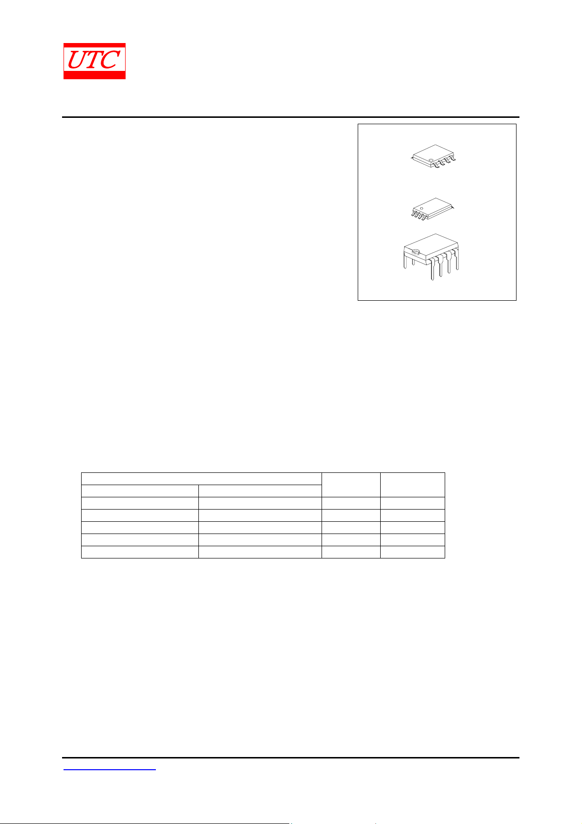
SOP-8
TSSOP-8
DIP-8
*Pb-free plating product number:LM386L
ORDERING INFORMATION
Order Number
Normal Lead Free Plating
LM386-S08-R LM386L-S08-R SOP-8 Tape Reel
LM386-S08-T LM386L-S08-T SOP-8 Tube
LM386-P08-R LM386L-P08-R TSSOP-8 Tape Reel
LM386-P08-T LM386L-P08-T TSSOP-8 Tube
LM386-D08-T LM386L-D08-T DIP-8 Tube
Package Packing
www.unisonic.com.tw 1
Copyright © 2005 Unisonic Technologies Co., QW-R107-007,F
Page 2
LM386 LINEAR INTEGRATED CIRCUIT
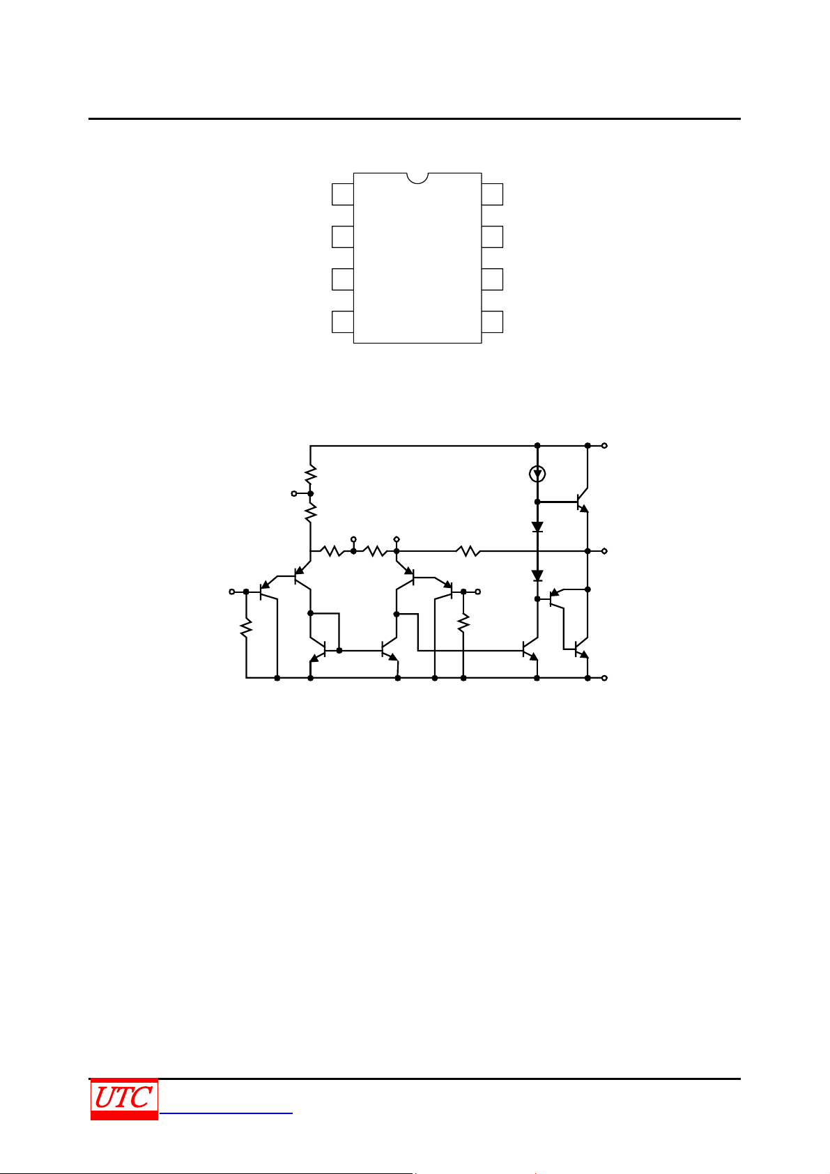
PIN CONFIGURATION
BLOCK DIAGRAM
BYPASS
2
-INPUT
Gain
-Input
+Input
7
15K
1
2
8
7
Gain
Bypass
UTC LM38 6
3
45
6
VCC
OutputGND
15K
GAINGAIN
8
150 1.35K
1
15K
3
+INPUT
6
Vs
5
OUT
V
50K
50K
4
GND
UNISONIC TECHNOLOGIES CO., LTD 2
www.unisonic.com.tw QW-R107-007. F
Page 3

LM386 LINEAR INTEGRATED CIRCUIT
ABSOLUTE MAXIMUM RATINGS
PARAMETER SYMBOL RATINGS UNIT
Supply Voltage VCC 15 V
Input Voltage VIN -0.4V ~ +0.4V V
DIP-8 1250
Power Dissipation
SOP-8 600
TSSOP-8
Operating Temperature T
Junction Temperature TJ +125 °C
Storage Temperature T
Note:1. Absolute maximum ratings are stress ratings only and functional device operation is not implied. The device
could be damaged beyond Absolute maximum ratings.
2. The device is guaranteed to meet performance specifications within 0 ℃~70℃ operating temperature range
and assured by design from –20℃~85℃.
ELECTRICAL CHARACTERISTICS (Ta=25°C, unless otherwise specified.)
PARAMETER SYMBOL TEST CONDITIONS MIN TYP MAX UNIT
Operating Supply Voltage Vss 4 12 V
Quiescent Current IQ Vss=6V, VIN=0 4 8 mA
Output Power P
OUT
Voltage Gain GV
Bandwidth BW Vss=6V , Pin1 and pin 8 open 300 kHz
Total Harmonic Distortion THD
Rejection Ratio RR
Input Resistance RIN 50 kΩ
Input Bias Current I
Vss=6V Pin2 and pin 3 open 250 nA
BIAS
PD
0 ~ +70 °C
OPR
-40 ~ +150 °C
STG
Vss=6V, RL=8Ω, THD=10%
Vss=9V, R
=8Ω, THD=10%
L
Vss=6V, f=1kHz
10µF from pin 1 to pin 8
P
=125mW, Vs=6V,f=1kHz
OUT
RL=8Ω pin1 and pin 8 open
Vss=6V, f=1kHz, C
BYPASS
=10µF
pin1and pin 8 open, Referred to
output
600
250
500
325
700
26
46
0.2 %
50 dB
mW
mW
mW
dB
dB
UNISONIC TECHNOLOGIES CO., LTD 3
www.unisonic.com.tw QW-R107-007. F
Page 4
LM386 LINEAR INTEGRATED CIRCUIT
APPLICATION NOTES
GAIN CONTROL
To make the LM386 a more versatile amplifier, two pins(1and 8) are provided for gain control. With pins 1 and 8
open the 1.35 kΩ resistor sets the gain at 20(26dB),If a capacitor is put from pin 1 to 8,bypassing the 1.35 kΩ
resistor, the gain will go up to 200(46dB).If a resistor is placed in series with the capacitor, the gain can be set to any
value from 20 to 200.Gain control can also be done by capacitively coupling a resistor (or FET) from pin 1 to ground.
Additional external components can be placed in parallel with the internal feedback resistors to tailor the gain and
frequency response for individual applications. For example we can compensate poor speaker bass response b y
frequency shaping the feedback path. This is done with a series RC from pin 1 to 5 (paralleling the internal 15 kΩ
resistor). For 6 dB effective bass boost: R=15 kΩ, the lowest value for good stable operation is R=10 k Ω, if pin 8 is
open, If pins 1 and 8 are bypassed then R as low as 2 kΩ can be used. This restriction is because the amplifier is
only compensated for closed-loop gains greater than 9.
INPUT BIASING
The schematic shows that both inputs are biased to ground with a 50 kΩ resistor. The base current of the input
transistors is about 250nA, so the inputs are at about 12.5mW when left open. If the dc source resistance driving the
LM386 is higher than 250 kΩ it will contribute very little additional offset (about 2.5mW at the input, 50mW at the
output).If the dc source resistance is less than 10 kΩ,then shorting the unused input to ground will keep the offset
low (about 2.5mV at the input,50 mV at the output).For dc source resistances between these values we can
eliminate excess offset by putting a resistor from the unused input to ground, equal in value to the dc source
resistance. Of course all offset problems are eliminated if the input is capacitively coupled.
When using the LM386 with higher gains (bypassing the 1.35 k Ω resistor between pins 1 and 8)it is necessary to
bypass the unused input, preventing degradation of gain and possible instabilities. This is done with a 0.1µF
capacitor or a short to ground depending on the dc source resistance on the driven input.
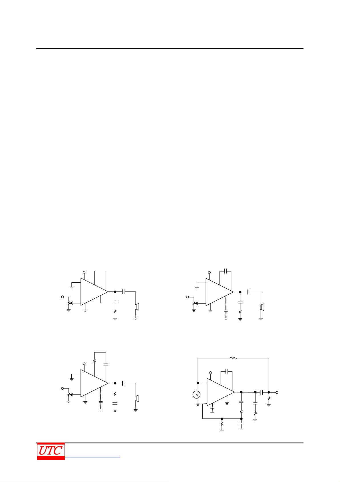
TYPICAL APPLICATIONS CIRCUIT
Amplifier with Gain=20
Minimum Parts
Vs
6
2
-
1
V
IN
10K
3
+
7
4
250µF
8
+
5
0.05µF
10
Amplifier with Gain=200
V
IN
10K
10µF
Vs
+
6
2
-
1
3
+
7
4
BYPASS
250µF
8
+
5
0.05µF
10
Amplifier with Gain=50
Vs
1.2K
6
2
-
V
IN
10K
3
+
4
10µF
1
7
BYPASS
250µF
8
+
5
10
0.05µF
ELDEMA
CF-S-2158
Low Distortion Power Wienbridge O scillator
10µF
Vs
+
6
2
-
1
4
3V-15mA
f=1kHz
3
+
4.7K
7
BYPASS
0.01µF
0.01µF
390
47K
8
5
50µF
+
0.05µF
10
V
o
R
L
UNISONIC TECHNOLOGIES CO., LTD 4
www.unisonic.com.tw QW-R107-007. F
Page 5
LM386 LINEAR INTEGRATED CIRCUIT
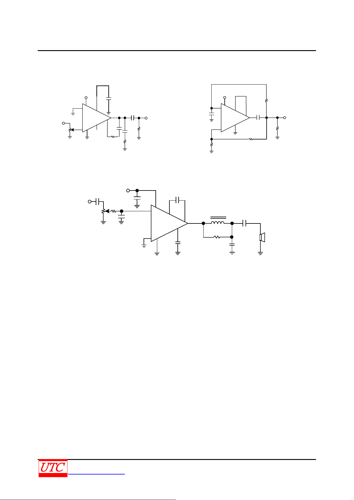
TYPICAL APPLICATIONS CIRCUIT(cont.)
Amplifier with Bass Boost
Square Ware Oscillator
10K
Vs
6
2
-
3
+
4
BYPASS
7
1
0.033µF
8
10K
250µF
+
5
0.05µF
10Ω
O
V
R
L
0.1µF
AM Radio Power Amplifier
FROM
DETECTOR
Cc
VOL
10K
R1
10K
Vs
0.05µ F
C1
2
-
2200pF
3
+
Note 1: Twist Supply lead and supply ground very tightly.
Note 2: Twist speaker lead and ground very tightly.
Note 3: Ferrite bead in Ferroxcube K5-001-001/3B with 3 turns of wire.
Note 4: R1C1 band limits input signals.
Note 5: All components must be spaced very closely to IC.
10µ F
+
6
1
8
5
7
4
+
10µ F
47
Vs
2
-
3
+
1K
FERRITE
BEAD
6
1
4
f=1kHz
250µ F
+
+
0.05µ F
8
5
10K
50µF
+
30K
V
R
L
8Ω
SPEAKER
O
UNISONIC TECHNOLOGIES CO., LTD 5
www.unisonic.com.tw QW-R107-007. F
Page 6
LM386 LINEAR INTEGRATED CIRCUIT
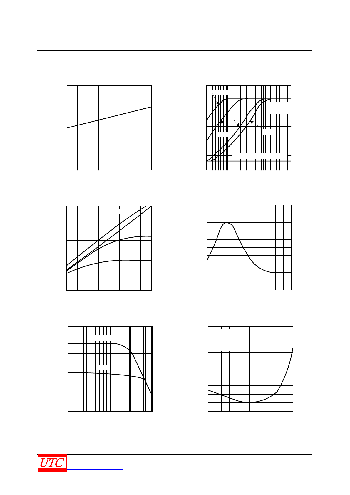
TYPICAL CHARACTERISTICS
Quiescent Supply Current vs Supply Voltage
6
5
4
3
Supply Current (mA)
2
Power Supply Rejection Ratio(Referred
to the Output) vs Frequency
60
C7=50µF
50
40
30
20
Power Supply Rejection (dB)
10
1µF
10µF
NO BYPASSCAPACITOR
Vs=6V
Av=26dB
0.5µF
1
4 5 6 7 8 9 101112
Supply Voltage(volts)
Peak-to -P eak Output Voltage Swing vs Supply Voltage
10
8
6
4
2
Output Voltage (Vol ts Peak-To-Peak)
0
456789101112
Supply Voltage(volts)
Voltage Gain vs Frequency
60
C
50
40
30
20
Voltage Gain (dB)
10
0
100 1K 10K 100K 1M
1.8
C
1.8
Frequency (Hz)
RL=∞
16
8
4
=10µF
=0
0
10 100 1K 10K 100K
Frequency (Hz)
Frequency Response With Bass Boost
27
26
25
24
23
22
21
20
Voltage Gain (dB)
19
18
17
20 50 100 200 5001K2K 5K10K
Frequency (Hz)
20K
Distortion vs Frequency
2.0
1.8
1.6
1.4
1.2
1.0
0.8
0.6
0.4
Total Harmonic Distortion (%)
0.2
0
Vs=6V
R
L
=8Ω
P
OUT
=125mW
1.8
Av=26dB(C
20 50 100200 5001K 2K 5K10K
=0)
Frequency (Hz)
20K
UNISONIC TECHNOLOGIES CO., LTD 6
www.unisonic.com.tw QW-R107-007. F
Page 7
LM386 LINEAR INTEGRATED CIRCUIT
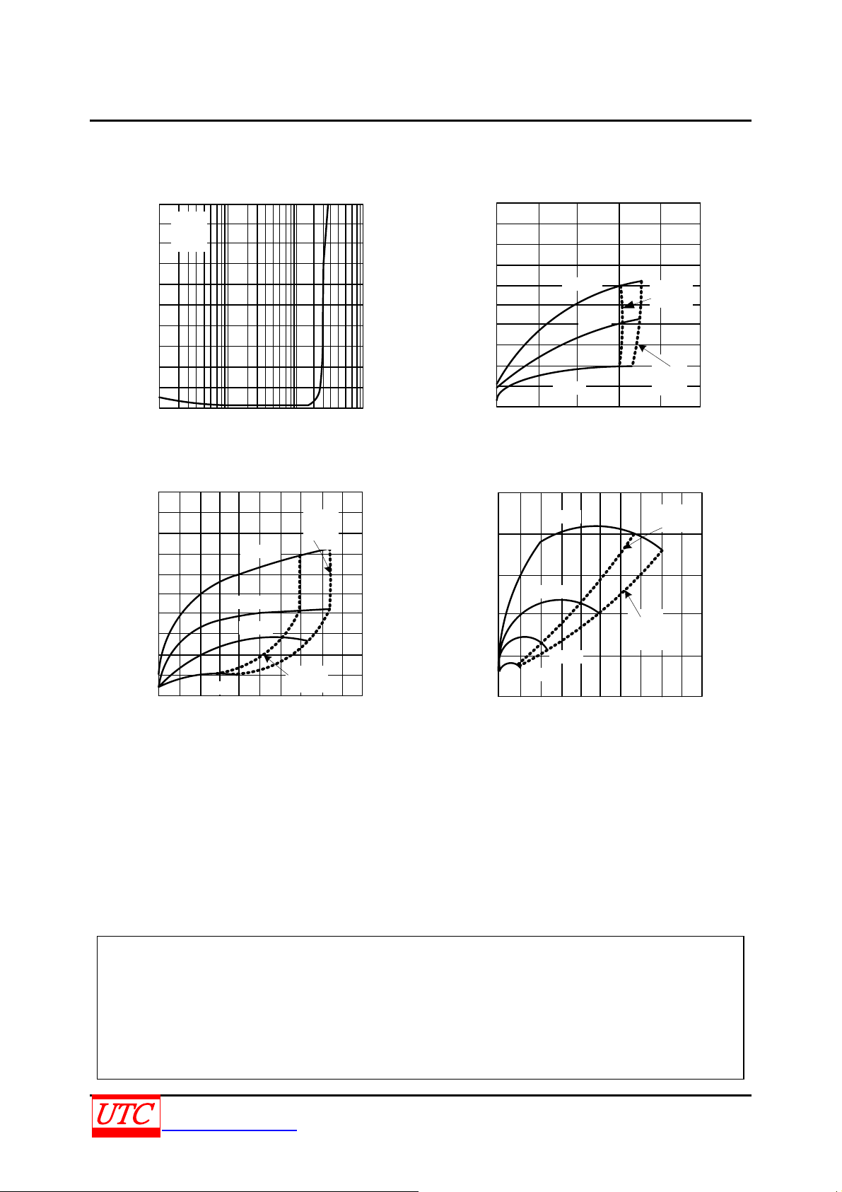
TYPICAL CHARACTERISTICS(cont.)
Distortion vs Output Power
10
Vs=6V
9
R
L
=8Ω
8
f=1kHz
7
6
5
4
3
2
Total Harmonic Distortion (%)
1
0
Power Output (Watts )
0.10.001 0.01 1.0
Device Dissipaton vs Output Power -
2.0
1.8
1.6
1.4
1.2
1.0
0.8
0.6
0.4
Device Dissipation (W)
0.2
0
0 0.1 0.2 0.3 0.4
4ΩLoad
Vs= 12V
Vs=9V
Vs=6V
O utput Power (W)
3% THD
LEVEL
10%
THD
LEVEL
0.5
Devic e Dissipaton vs Output Power -
2.0
1.8
1.6
1.4
1.2
1.0
0.8
0.6
0.4
Device Dissipation (W)
0.2
0
0 0.1 0.2 0.3 0.4
8ΩLoad
Vs=16V
Vs= 12V
Vs=9V
Vs=6V
0.5
Output Power (W)
10%
THD
LEVEL
3% THD
LEVEL
0.60.7 0.80.91.0
Devic e Dissipaton vs Output Power -16ΩLoad
1.0
3% THD
LEVEL
10%
THD
LEVEL
1.2 1.4 1.6 1 .8 2.0
0.8
0.6
0.4
0.2
Device Dissipation (W)
0
0 0 .2 0.4 0.60.8
Vs=16V
Vs= 12V
Vs=9V
Vs=6V
1.0
Output Power (W)
UTC assumes no responsibility for equipment failures that result from using products at values that
exceed, even momentarily, rated values (such as maximum ratings, operating condition ranges, or
other parameters) listed in products specifications of any and all UT C products described or contained
herein. UTC products are not designed f or use in life support appliances, devi ces or systems where
malf unction of these products can be reasonably expected to result in personal injury. Reproduction in
whole or in part is prohibited without the prior written consent of the copyright owner. The information
presented in this document does not form part of any quotation or contract, is believ ed to be accurate
and reliable and may be c hanged without notice.
UNISONIC TECHNOLOGIES CO., LTD 7
www.unisonic.com.tw QW-R107-007. F
 Loading...