

Datasheet LM385PS-1.2, LM385BDR-1-2, LM385D-1-2, LM385LPR-1-2, LM385LP-1-2 Datasheet (Texas Instruments)
...Page 1
LM285-1.2, LM385-1.2, LM385B-1.2
MICROPOWER VOLTAGE REFERENCES
SLVS075C – APRIL 1989 – REVISED JULY 1999
1
POST OFFICE BOX 655303 • DALLAS, TEXAS 75265
D
Operating Current Range
– LM285 . . . 10 µA to 20 mA
– LM385 . . . 15 µA to 20 mA
– LM385B ...15 µA to 20 mA
D
1% and 2% Initial Voltage Tolerance
D
Reference Impedance
– LM385...1 Ω Max at 25°C
– All Devices . . . 1.5 Ω Max Over Full
T emperature Range
D
Very Low Power Consumption
D
Applications:
– Portable Meter References
– Portable Test Instruments
– Battery-Operated Systems
– Current-Loop Instrumentation
– Panel Meters
D
Designed to be Interchangeable With
National LM285-1.2 and LM385-1.2
description
These micropower, two-terminal, band-gap voltage references operate over a 10-µA to 20-mA current range
and feature exceptionally low dynamic impedance and good temperature stability . On-chip trimming provides
tight voltage tolerance. The band-gap reference for these devices has low noise and long-term stability.
The design makes these devices exceptionally tolerant of capacitive loading and thus, easier to use in most
reference applications. The wide dynamic operating temperature range accommodates varying current
supplies with excellent regulation.
The extremely low power drain of this series makes them useful for micropower circuitry. These voltage
references can be used to make portable meters, regulators, or general-purpose analog circuitry , with battery
life approaching shelf life. The wide operating current range allows them to replace older references with
tighter-tolerance parts.
The LM285-1.2 is characterized for operation from –40°C to 85°C. The LM385-1.2 and LM385B-1.2 are
characterized for operation from 0°C to 70°C.
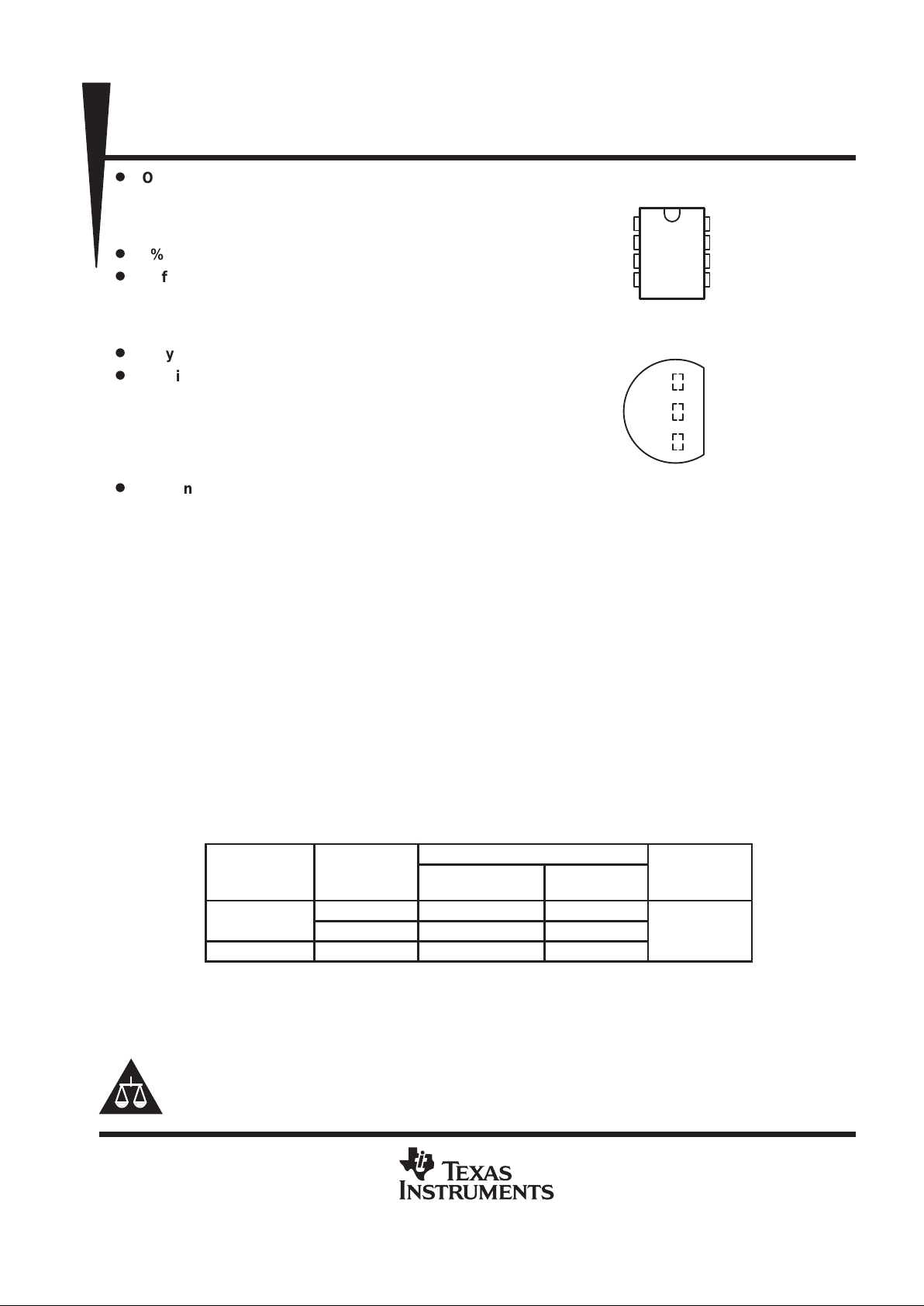
AVAILABLE OPTIONS
PACKAGED DEVICES
†
T
A
V
Z
TOLERANCE
SMALL OUTLINE
(D)
PLASTIC
(LP)
CHIP FORM
(Y)
°
°
2% LM385D-1.2 LM385LP-1.2
0°C to 70°C
1% LM385BD-1.2 LM385BLP-1.2
LM385Y-1.2
–40°C to 85°C 1% LM285D-1.2 LM285LP-1.2
The D package is available taped and reeled. Add the suffix R to the device type (e.g., LM385DR-1-2).
The chip form is tested at TA = 25°C.
†
For ordering purposes, the decimal point in the part number must be replaced with a hyphen (i.e., show
the -1.2 suffix as “-1-2”).
Copyright 1999, Texas Instruments Incorporated
PRODUCTION DATA information is current as of publication date.
Products conform to specifications per the terms of Texas Instruments
standard warranty. Production processing does not necessarily include
testing of all parameters.
Please be aware that an important notice concerning availability, standard warranty, and use in critical applications of
Texas Instruments semiconductor products and disclaimers thereto appears at the end of this data sheet.
1
2
3
4
8
7
6
5
NC
NC
NC
ANODE
CATHODE
NC
NC
NC
D PACKAGE
(TOP VIEW)
NC–No internal connection
LP PACKAGE
(TOP VIEW)
ANODE
CATHODE
NC
Page 2

LM285-1.2, LM385-1.2, LM385B-1.2
MICROPOWER VOLTAGE REFERENCES
SLVS075C – APRIL 1989 – REVISED JULY 1999
2
POST OFFICE BOX 655303 • DALLAS, TEXAS 75265
symbol
ANODE
CATHODE
schematic
CATHODE
Q13
Q12
Q7
Q4
600 kΩ
7.5 kΩ
ANODE
200 kΩ
50 kΩ
300 kΩ
Q14
20 pF20 pF
Q11
Q10
Q9
Q5
Q3
Q1
Q2
Q8Q6
60 kΩ500 Ω100 kΩ
NOTE A: Component values shown are nominal.
absolute maximum ratings over operating free-air temperature range
†
Reverse current, IR 30 mA. . . . . . . . . . . . . . . . . . . . . . . . . . . . . . . . . . . . . . . . . . . . . . . . . . . . . . . . . . . . . . . . . . . . . .
Forward current, IF 10 mA. . . . . . . . . . . . . . . . . . . . . . . . . . . . . . . . . . . . . . . . . . . . . . . . . . . . . . . . . . . . . . . . . . . . . . .
Package thermal impedance, θJA (see Notes 1 and 2): D package 197°C/W. . . . . . . . . . . . . . . . . . . . . . . . . . .
LP package 156°C/W. . . . . . . . . . . . . . . . . . . . . . . . . .
Lead temperature 1,6 mm (1/16 inch) from case for 10 seconds 260°C. . . . . . . . . . . . . . . . . . . . . . . . . . . . . . .
Storage temperature range, T
stg
–65°C to 150°C. . . . . . . . . . . . . . . . . . . . . . . . . . . . . . . . . . . . . . . . . . . . . . . . . . .
†
Stresses beyond those listed under “absolute maximum ratings” may cause permanent damage to the device. These are stress ratings only, and
functional operation of the device at these or any other conditions beyond those indicated under “recommended operating conditions” is not
implied. Exposure to absolute-maximum-rated conditions for extended periods may affect device reliability.
NOTES: 1. Maximum power dissipation is a function of T
J(max)
,
θ
JA
, and TA. The maximum allowable power dissipation at any allowable ambient
temperature is PD = (T
J(max)
– TA)/
θ
JA
. Operation at the absolute maximum TJ of 150°C can impact reliability.
2. The package thermal impedance is calculated in accordance with JESD51, except for through-hole packages which use a trace
length of zero.
recommended operating conditions
MIN MAX UNIT
Reference current, I
Z
0.01 20 mA
p
p
LM285-1.2 –40 85
°
Operating free-air temperature range, T
A
LM385-1.2, LM385B-1.2 0 70
°C
Page 3
LM285-1.2, LM385-1.2, LM385B-1.2
MICROPOWER VOLTAGE REFERENCES
SLVS075C – APRIL 1989 – REVISED JULY 1999
3
POST OFFICE BOX 655303 • DALLAS, TEXAS 75265
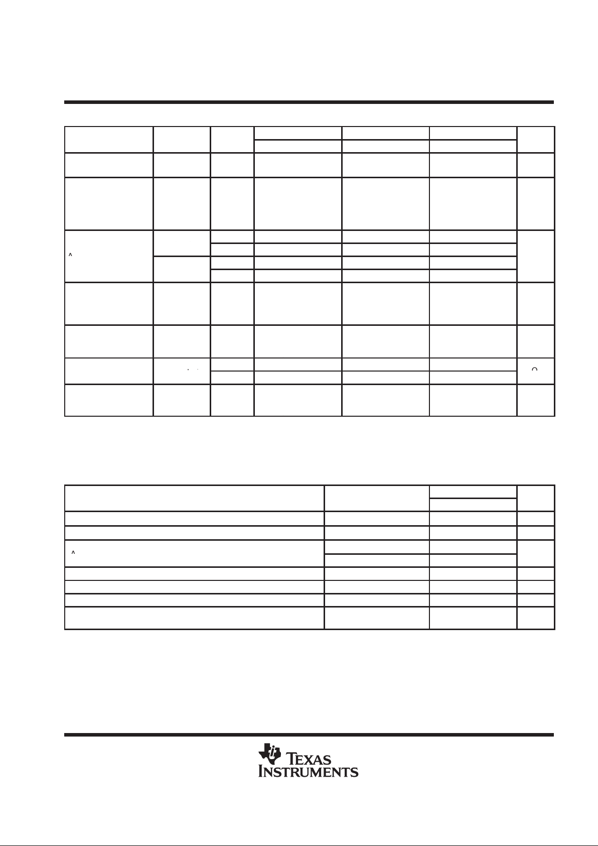
electrical characteristics at specified free-air temperature
TEST
LM285-1.2 LM385-1.2 LM385B-1.2
PARAMETER
CONDITIONS
T
A
†
MIN TYP MAX MIN TYP MAX MIN TYP MAX
UNIT
V
Z
Reference
voltage
IZ = I(min)
to 20 mA
‡
25°C 1.223 1.235 1.247 1.21 1.235 1.26 1.223 1.235 1.247 V
α
VZ
Average
temperature
coefficient of
reference
voltage
§
IZ = I(min)
to 20 mA
‡
25°C ±20 ±20 ±20 ppm/°C
I
= I(min)
25°C 1 1 1
Change in
reference
Z
()
to 1 mA
‡
Full range 1.5 1.5 1.5
∆V
Z
voltage with
I
= 1 mA
25°C 12 20 20
mV
current
Z
to 20 mA
Full range 30 30 30
∆VZ/∆t
Long-term
change in
reference
voltage
IZ = 100 µA 25°C ±20 ±20 ±20 ppm/khr
IZ(min)
Minimum
reference
current
Full range 8 10 8 15 8 15 µA
Reference I
= 100 µA,
25°C 0.2 0.6 0.4 1 0.4 1
z
z
impedance
Z
µ ,
f = 25 Hz
Full range 1.5 1.5 1.5
Ω
V
n
Broadband
noise voltage
IZ = 100 µA,
f = 10 Hz to
10 kHz
25°C 60 60 60 µV
†
Full range is –40°C to 85°C for the LM285-1.2, and 0°C to 70°C for the LM385-1.2 and LM385B-1.2.
‡
I(min) = 10 µA for the LM285-1.2 and 15 µA for the LM385-1.2 and LM385B-1.2.
§
The average temperature coefficient of reference voltage is defined as the total change in reference voltage divided by the specified temperature
range.
electrical characteristics, TA = 25°C
LM385Y-1.2
PARAMETER
TEST CONDITIONS
MIN TYP MAX
UNIT
V
Z
Reference voltage
IZ = 15 µA to 20 mA
1.21 1.235 1.26 V
α
VZ
Average temperature coefficient of reference voltage
§
IZ = 15 µA to 20 mA
±20 ppm/°C
IZ = 15 µA to 1 mA
1
∆VZChange in reference voltage with current
IZ = 1 mA to 20 mA 20
mV
∆VZ/∆t Long-term change in reference voltage IZ = 100 µA ±20 ppm/khr
IZ(min) Minimum reference current 8 15 µA
z
z
Reference impedance IZ = 100 µA 0.4 1 Ω
V
n
Broadband noise voltage
IZ = 100 µA,
f = 10 Hz to 10 kHz
60 µV
§
The average temperature coefficient of reference voltage is defined as the total change in reference voltage divided by the specified temperature
range.
Page 4

LM285-1.2, LM385-1.2, LM385B-1.2
MICROPOWER VOLTAGE REFERENCES
SLVS075C – APRIL 1989 – REVISED JULY 1999
4
POST OFFICE BOX 655303 • DALLAS, TEXAS 75265
TYPICAL CHARACTERISTICS
†
Figure 1
0 0.2 0.4 0.6 0.8 1 1.2 1.4
TA = –55°C to 125°C
– Reverse Current –
VR – Reverse Voltage – V
0.1
1
10
100
REVERSE CURRENT
vs
REVERSE VOLTAGE
I
R
Aµ
Figure 2
1010.10.01
–4
0
4
8
12
16
IR – Reverse Current – mA
– Reference Voltage Change – mV
REFERENCE VOLTAGE CHANGE
vs
REVERSE CURRENT
100
∆V
Z
TA = –55°C to 125°C
FORWARD VOLTAGE
vs
FORWARD CURRENT
Figure 3
0.01 0.1 1 10 100
0.8
1.2
0.4
0
IF – Forward Current – mA
– Forward Voltage – VV
F
TA = 25°C
Figure 4
105 125856545255–15–35–55
1.225
1.23
1.235
1.24
1.245
TA – Free-Air Temperature – °C
– Reference Voltage – V
REFERENCE VOLTAGE
vs
FREE-AIR TEMPERATURE
V
Z
1.220
†
Data at high and low temperatures are applicable only within the rated operating free-air temperature ranges of the various devices.
Page 5

LM285-1.2, LM385-1.2, LM385B-1.2
MICROPOWER VOLTAGE REFERENCES
SLVS075C – APRIL 1989 – REVISED JULY 1999
5
POST OFFICE BOX 655303 • DALLAS, TEXAS 75265
TYPICAL CHARACTERISTICS
†
Figure 5
REFERENCE IMPEDANCE
vs
REFERENCE CURRENT
IZ – Reference Current – mA
TA = –55°C to 125°C
f = 25 Hz
100
10
1
0.1
1001010.10.01
z
z
– Reference Impedance –
Ω
Figure 6
NOISE VOLTAGE
vs
FREQUENCY
Vn – Noise Voltage – nV/
f – Frequency – Hz
700
600
500
400
300
200
100
0
10 100 1 k 10 k 100 k
√
Hz
IZ = 100 µA
TA = 25°C
V
n
Output Noise Voltage –
f – Cutoff Frequency – kHz
1001010.1
70
60
50
40
30
20
10
0
IZ = 100 µA
TA = 25°C
OUTPUT NOISE VOLTAGE
vs
CUTOFF FREQUENCY
RC Low Pass
µV
C
R
100 µA
Figure 7 Figure 8
Input
V
I
t – Time – µs
Input and Output Voltages – V
0 100 500 600
0
5
0
0.5
1
1.5
V
O
36 kΩ
TRANSIENT RESPONSE
Output
†
Data at high and low temperatures are applicable only within the rated operating free-air temperature ranges of the various devices.
Page 6

LM285-1.2, LM385-1.2, LM385B-1.2
MICROPOWER VOLTAGE REFERENCES
SLVS075C – APRIL 1989 – REVISED JULY 1999
6
POST OFFICE BOX 655303 • DALLAS, TEXAS 75265
APPLICATION INFORMATION
+
412 Ω
‡
±1%
†
Adjust for 11.15 mV at 25°C across 953 Ω
‡
Adjust for 12.17 mV at 25°C across 412 Ω
2.00 kΩ ±1%
IO ≈ 58 µA
+
5.1 kΩ
R
LM334
V–
V+
100 kΩ ±1%
10 kΩ
953 Ω
†
±1%
Meter
Type K
LM385-1.2
Mercury Cell
1.345 V
–
–
500 Ω
cw
cw
Figure 9. Thermocouple Cold-Junction Compensator
2.3 V ≤ V+ ≤ 30 V
R
V–
V+
2.74 kΩ
1.2 V
LM385-1.2
LM334
Figure 10. Operation Over a Wide Supply Range
LM385-1.2
1.2 V
499 kΩ
9 V
Figure 11. Reference From a 9-V Battery
Page 7

IMPORTANT NOTICE
T exas Instruments and its subsidiaries (TI) reserve the right to make changes to their products or to discontinue
any product or service without notice, and advise customers to obtain the latest version of relevant information
to verify, before placing orders, that information being relied on is current and complete. All products are sold
subject to the terms and conditions of sale supplied at the time of order acknowledgement, including those
pertaining to warranty, patent infringement, and limitation of liability.
TI warrants performance of its semiconductor products to the specifications applicable at the time of sale in
accordance with TI’s standard warranty. Testing and other quality control techniques are utilized to the extent
TI deems necessary to support this warranty. Specific testing of all parameters of each device is not necessarily
performed, except those mandated by government requirements.
CERT AIN APPLICATIONS USING SEMICONDUCTOR PRODUCTS MAY INVOLVE POTENTIAL RISKS OF
DEATH, PERSONAL INJURY, OR SEVERE PROPERTY OR ENVIRONMENTAL DAMAGE (“CRITICAL
APPLICATIONS”). TI SEMICONDUCTOR PRODUCTS ARE NOT DESIGNED, AUTHORIZED, OR
WARRANTED TO BE SUITABLE FOR USE IN LIFE-SUPPORT DEVICES OR SYSTEMS OR OTHER
CRITICAL APPLICATIONS. INCLUSION OF TI PRODUCTS IN SUCH APPLICA TIONS IS UNDERSTOOD T O
BE FULLY AT THE CUSTOMER’S RISK.
In order to minimize risks associated with the customer’s applications, adequate design and operating
safeguards must be provided by the customer to minimize inherent or procedural hazards.
TI assumes no liability for applications assistance or customer product design. TI does not warrant or represent
that any license, either express or implied, is granted under any patent right, copyright, mask work right, or other
intellectual property right of TI covering or relating to any combination, machine, or process in which such
semiconductor products or services might be or are used. TI’s publication of information regarding any third
party’s products or services does not constitute TI’s approval, warranty or endorsement thereof.
Copyright 1999, Texas Instruments Incorporated
 Loading...