

Page 1
LM383/LM383A 7W Audio Power Amplifier
LM383/LM383A 7W Audio Power Amplifier
February 1995
General Description
The LM383 is a cost effective, high power amplifier suited
for automotive applications. High current capability (3.5A)
enables the device to drive low impedance loads with low
distortion. The LM383 is current limited and thermally protected. High voltage protection is available (LM383A) which
enables the amplifier to withstand 40V transients on its supply. The LM383 comes in a 5-pin TO-220 package.
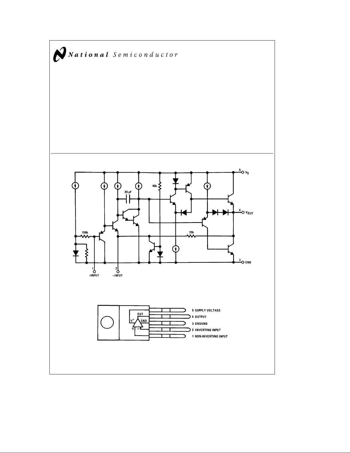
Equivalent Schematic
Features
Y
High peak current capability (3.5A)
Y
Large output voltage swing
Y
Externally programmable gain
Y
Wide supply voltage range (5V–20V)
Y
Few external parts required
Y
Low distortion
Y
High input impedance
Y
No turn-on transients
Y
High voltage protection available (LM383A)
Y
Low noise
Y
AC short circuit protected
TL/H/7145– 1
Connection Diagram
Plastic Package
Order Number LM383T or LM383AT
See NS Package Number T05B
C
1995 National Semiconductor Corporation RRD-B30M115/Printed in U. S. A.
TL/H/7145
TL/H/7145– 2
Page 2
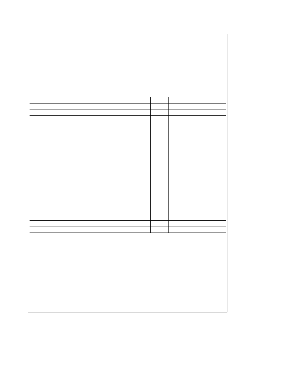
Absolute Maximum Ratings
If Military/Aerospace specified devices are required,
please contact the National Semiconductor Sales
Office/Distributors for availability and specifications.
Peak Supply Voltage (50 ms)
LM383A (Note 2) 40V
LM383 25V
Operating Supply Voltage 20V
Output Current
Repetitive 3.5A
Non-repetitive 4.5A
Input Voltage
g
0.5V
Power Dissipation (Note 3) 15W
Operating Temperature 0§Ctoa70§C
b
Storage Temperature
60§Ctoa150§C
Lead Temperature (Soldering, 10 sec.) 260§C
Electrical Characteristics V
S
e
14.4V, T
TAB
e
25§C, A
e
100 (40 dB), R
V
e
4X, unless otherwise specified
L
Parameter Conditions Min Typ Max Units
DC Output Level 6.4 7.2 8 V
Quiescent Supply Current Excludes Current in Feedback Resistors 45 80 mA
Supply Voltage Range 5 20 V
Input Resistance 150 kX
Bandwidth Gaine40 dB 30 kHz
Output Power V
THD P
Ripple Rejection R
Input Noise Voltage R
Input Noise Current R
Note 1: A 0.2 mF capacitor in series with a 1X resistor should be placed as close as possible to pins 3 and 4 for stability.
Note 2: The LM383 shuts down above 25V.
Note 3: For operating at elevated temperatures, the device must be derated based on a 150
junction to case.
e
13.2V, fe1 kHz
S
e
R
4X, THDe10% 4.7 W
L
e
R
2X, THDe10% 7.2 W
L
e
V
13.8V, fe1 kHz
S
e
R
4X, THDe10% 5.1 W
L
e
R
2X, THDe10% 7.8 W
L
e
V
14.4V, fe1 kHz
S
e
R
4X, THDe10% 4.8 5.5 W
L
e
R
2X, THDe10% 7 8.6 W
L
e
R
1.6X, THDe10% 9.3 W
L
e
V
16V, fe1 kHz
S
e
R
4X, THDe10% 7 W
L
e
R
2X, THDe10% 10.5 W
L
e
R
1.6X, THDe10% 11 W
L
e
o
e
P
o
e
S
e
R
S
e
S
e
S
e
2W, R
4W, R
4X,fe1 kHz 0.2 %
L
e
2X,fe1 kHz 0.2 %
L
50X,fe100 Hz 30 40 dB
50X,fe1 kHz 44 dB
0, 15 kHz Bandwidth 2 mV
100 kX, 15 kHz Bandwidth 40 pA
C maximum junction temperature and a thermal resistance of 4§C/W
§
2
Page 3

Typical Performance Characteristics
Device Dissipation vs
Ambient Temperature
Open Loop Gain
vs Frequency
Output Power vs
Supply Voltage
Power Dissipation vs
Output Power
Supply Ripple Rejection
vs Frequency
Distortion vs Output Power Distortion vs Frequency
Power Dissipation vs
Output Power
Supply Current vs
Supply Voltage
Distortion vs Frequency Supply Voltage
Output Swing vs
3
TL/H/7145– 4
Page 4

Typical Applications
Single Amplifier
TL/H/7145– 3
16W Bridge Amplifier
Component Layout
Single Amplifier
e
V
20V
S
e
R
4X
L
Heatsink from:
Staver Company
41 Saxon Ave.
P.O. Drawer H
Bay Shore, NY 11706
Tel: (516) 666-8000 TL/H/7145– 6
4
TL/H/7145– 5
Page 5

Physical Dimensions inches (millimeters)
LM383/LM383A 7W Audio Power Amplifier
Order Number LM383T or LM383AT
NS Package Number T05B
LIFE SUPPORT POLICY
NATIONAL’S PRODUCTS ARE NOT AUTHORIZED FOR USE AS CRITICAL COMPONENTS IN LIFE SUPPORT
DEVICES OR SYSTEMS WITHOUT THE EXPRESS WRITTEN APPROVAL OF THE PRESIDENT OF NATIONAL
SEMICONDUCTOR CORPORATION. As used herein:
1. Life support devices or systems are devices or 2. A critical component is any component of a life
systems which, (a) are intended for surgical implant support device or system whose failure to perform can
into the body, or (b) support or sustain life, and whose be reasonably expected to cause the failure of the life
failure to perform, when properly used in accordance support device or system, or to affect its safety or
with instructions for use provided in the labeling, can effectiveness.
be reasonably expected to result in a significant injury
to the user.
National Semiconductor National Semiconductor National Semiconductor National Semiconductor
Corporation Europe Hong Kong Ltd. Japan Ltd.
1111 West Bardin Road Fax: (
Arlington, TX 76017 Email: cnjwge@tevm2.nsc.com Ocean Centre, 5 Canton Rd. Fax: 81-043-299-2408
Tel: 1(800) 272-9959 Deutsch Tel: (
Fax: 1(800) 737-7018 English Tel: (
National does not assume any responsibility for use of any circuitry described, no circuit patent licenses are implied and National reserves the right at any time without notice to change said circuitry and specifications.
Fran3ais Tel: (
Italiano Tel: (
a
49) 0-180-530 85 86 13th Floor, Straight Block, Tel: 81-043-299-2309
a
49) 0-180-530 85 85 Tsimshatsui, Kowloon
a
49) 0-180-532 78 32 Hong Kong
a
49) 0-180-532 93 58 Tel: (852) 2737-1600
a
49) 0-180-534 16 80 Fax: (852) 2736-9960
 Loading...