

Page 1
September 2006
LM3743
N-Channel FET Synchronous Buck Controller for Low
Output Voltages
Reference accuracy: ±1.75%, over full temperature and
General Description
The LM3743 is a voltage mode PWM buck controller which
implements synchronous rectification. It provides a low cost,
fault tolerant, and efficient point of load solution. To reduce
component count several parameters are fixed, such as
switching frequency and the short circuit protection level. For
example the LM3743 has an operating switching frequency
of 300 kHz or 1 MHz and a fixed 500 mV high side current
limit for switch node short-circuit protection. LM3743 is a very
fault tolerant IC with switch node short-circuit, output undervoltage protection, and the ability to self recover after the
removal of the fault. It avoids the need to over design components due to thermal runaway during a fault condition, thus
resulting in a lower cost solution. It employs a proprietary
monotonic glitch free pre-bias start-up method suited for FPGAs and ASIC logic devices. A 0.8V internal reference with
±1.75% accuracy is ideal for sub-volt conversion. An external
programmable soft-start allows for tracking and timing flexibility. The driver features 1.6Ω of pull-up resistance and 1Ω
of pull-down drive resistance for high power density and very
efficient power processing.
Features
Input voltage from 3.0V to 5.5V
■
Output voltage adjustable down to 0.8V
■
■
input voltage range
Low-side sensing programmable current limit
■
Fixed high-side sensing for supplemental short-circuit
■
protection
Undervoltage protection
■
Hiccup mode protection eliminates thermal runaway
■
during fault conditions
Externally programmable soft-start with tracking capability
■
Switching frequency options of 1 MHz or 300 kHz
■
Pre-bias start-up capability
■
MSOP-10 package
■
Applications
ASIC/FPGA/DSP core power
■
Broadband Communications
■
Multi-media Set Top Boxes
■
Networking Equipment
■
Printers/Scanners
■
Servers
■
Low Voltage Distributed Power
■
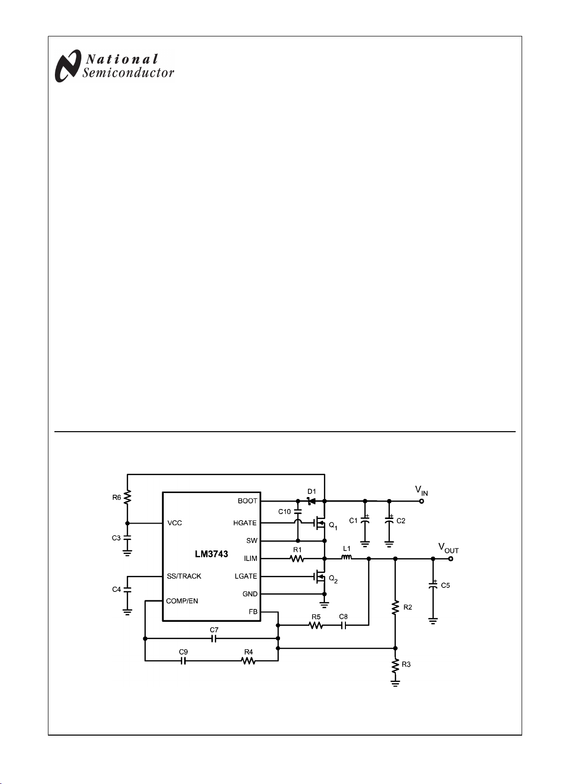
LM3743 N-Channel FET Synchronous Buck Controller for Low Output Voltages
Typical Application
20177401
© 2007 National Semiconductor Corporation 201774 www.national.com
Page 2
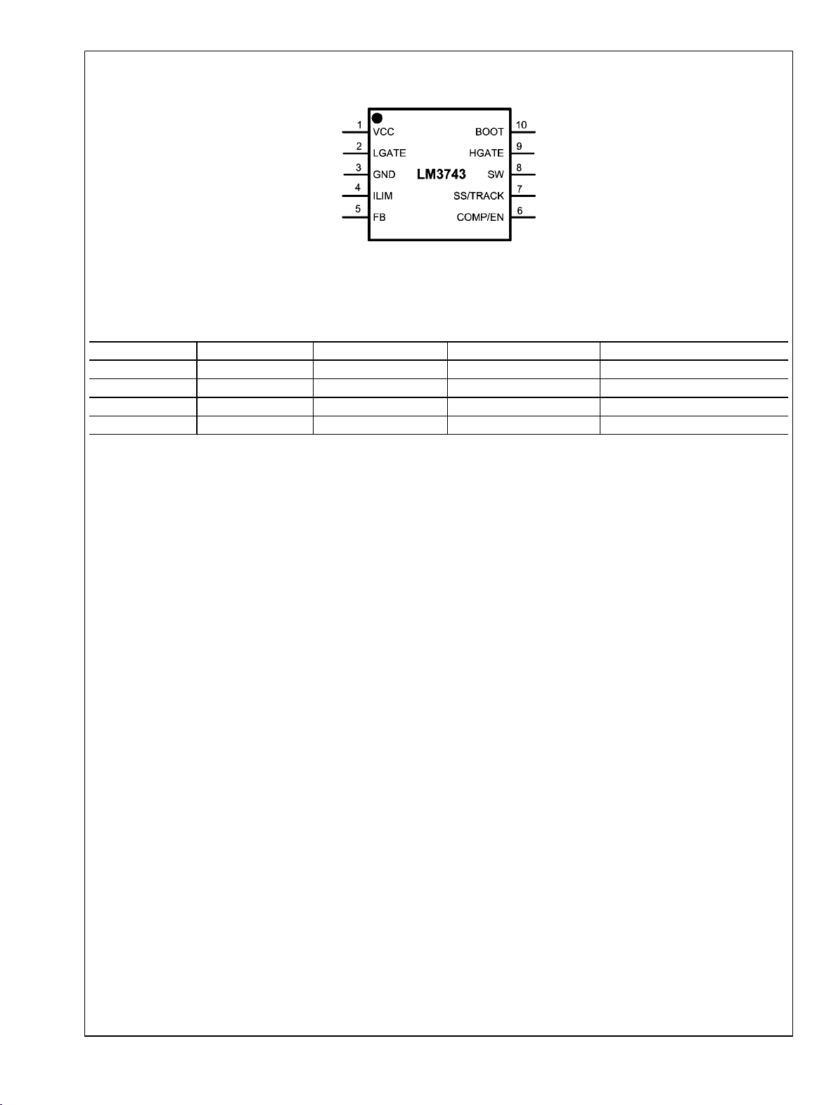
Connection Diagram
LM3743
10-Lead Plastic MSOP
NS Package Number MUB10A
Top View
20177402
Ordering Information
Order Number Frequency Option Top Mark NSC Package Drawing Supplied As
LM3743MM-300 300 kHz SKPB MUB10A 1000 units in Tape and Reel
LM3743MMX-300 300 kHz SKPB MUB10A 3500 units in Tape and Reel
LM3743MM-1000 1 MHz SKNB MUB10A 1000 units in Tape and Reel
LM3743MMX-1000 1 MHz SKNB MUB10A 3500 units in Tape and Reel
Pin Descriptions
VCC (Pin 1) Supply rail for the controller section of the IC. A
minimum capacitance of 1 µF, preferably a multi-layer ceramic capacitor type (MLCC), must be connected as close as
possible to the VCC and GND pin and a 1 to 4.99Ω resistance
must be connected in series from the supply rail to the Vcc
pin. See VCC FILTERING in the Design Consideration section for further details.
LGATE (Pin 2) Gate drive for the low-side N-channel MOSFET. This signal is interlocked with HGATE to avoid a shootthrough problem.
GND (Pin 3) Power ground (PGND) and signal ground
(SGND). Connect the bottom feedback resistor between this
pin and the feedback pin.
ILIM (Pin 4) Low side current limit threshold setting pin. This
pin sources a fixed 50 µA current. A resistor of appropriate
value should be connected between this pin and the drain of
the low-side N-FET.
FB (Pin 5) Feedback pin. This is the inverting input of the error
amplifier used for sensing the output voltage and compensating the control loop.
COMP/EN (Pin 6) Output of the error amplifier and enable
pin. The voltage level on this pin is compared with an internally
generated ramp signal to determine the duty cycle. This pin
is necessary for compensating the control loop. Forcing this
pin to ground will shut down the IC.
SS/TRACK (Pin 7) Soft-start and tracking pin. This pin is
connected to the non-inverting input of the error amplifier during initial soft-start, or any time the voltage is below the
reference. To track the rising ramp of another power supply's
output, connect a resistor divider from the output of that supply to this pin as described in Application Information.
SW (Pin 8) Switch pin. The lower rail of the high-side N-FET
driver. Also used for the high side current limit sensing.
HGATE (Pin 9) Gate drive for the high-side N-channel MOSFET. This signal is interlocked with LGATE to avoid a shootthrough problem.
BOOT (Pin 10) Supply rail for the N-channel MOSFET high
gate drive. The voltage should be at least one gate threshold
above the regulator input voltage to properly turn on the highside N-FET. See MOSFET Gate Drivers in the Application
Information section for more details on how to select MOSFETs.
www.national.com 2
Page 3
LM3743
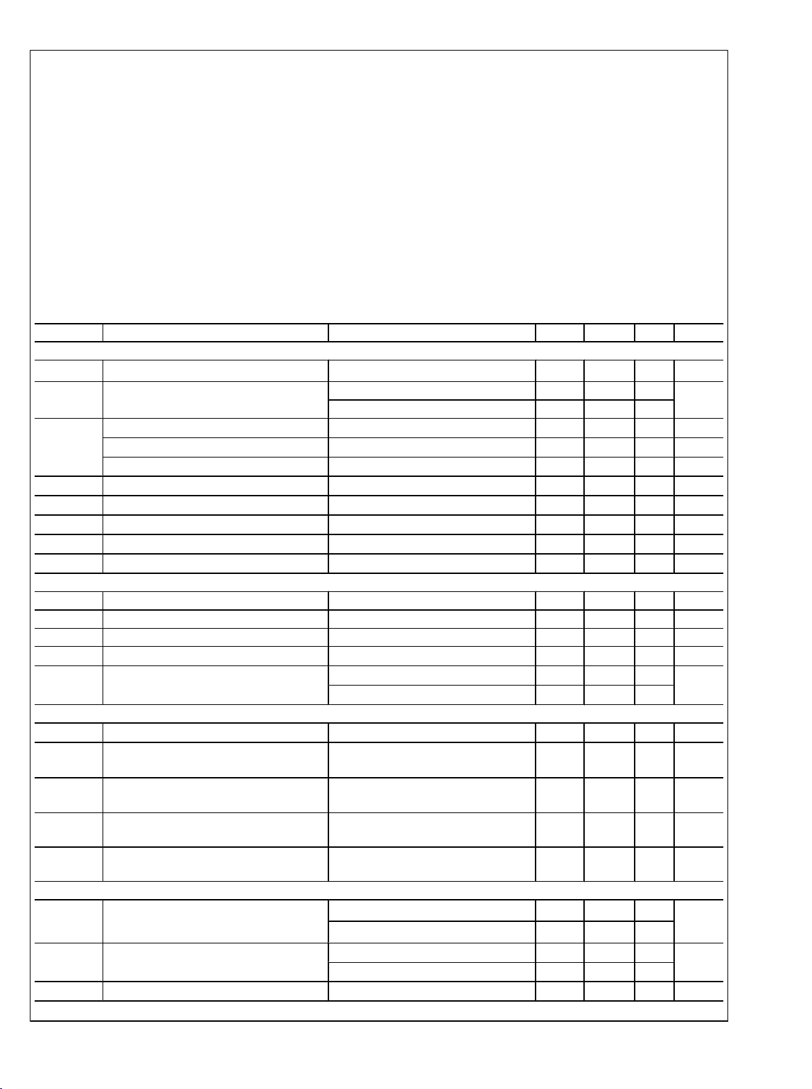
Absolute Maximum Ratings (Note 1)
If Military/Aerospace specified devices are required,
please contact the National Semiconductor Sales Office/
Distributors for availability and specifications.
V
CC
SW to GND -0.3V to 6V
Boot to GND -0.3V to 12V
Boot to SW -0.3V to 6V
SS/TRACK, ILIM, COMP/EN,FB
to GND
-0.3V to 6V
-0.3V to V
CC
Storage Temperature −65°C to 150°C
Soldering Information
Lead Temperature (soldering, 10sec) 260°C
Infrared or Convection (20sec) 235°C
ESD Rating (Note 3) + / – 2 kV
Operating Ratings
Supply Voltage Range, VCC (Note 2)
Junction Temperature Range (TJ)
3.0V to 5.5V
−40°C to +125°C
Junction Temperature 150°C
Electrical Characteristics V
= 3.3V, COMP/EN floating unless otherwise indicated in the conditions column.
CC
Limits in standard type are for TJ = 25°C only; limits in boldface type apply over the junction temperature (TJ) range of -40°C to
+125°C. Minimum and Maximum limits are guaranteed through test, design, or statistical correlation. Typical values represent the
most likely parametric norm at TJ = 25°C, and are provided for reference purposes only.
Symbol Parameter Conditions Min Typ Max Units
SYSTEM PARAMETERS
V
V
UVLO
FB pin voltage in regulation
FB
3.0V ≤ VCC ≤ 5.5V
0.786 0.8 0.814 V
UVLO thresholds Input voltage rising 2.84 3.0
Input voltage falling 2.45 2.66
I
VCC
Operating VCC current fSW = 300 kHz, LM3743-300 1.5 2.5 mA
Operating VCC current fSW = 1 MHz, LM3743-1000 1.8 3.0 mA
Shutdown VCC current COMP/EN = 0V 6 50 µA
I
SS/TRACK
I
ILIM
V
ILIM
I
COMP/EN
V
HS-CLIM
SS/TRACK pin source current V
ILIM pin source current V
SS/TRACK
ILIM
= 0V 8 10.2 12.5 µA
= 0V 42.5 50 57.5 µA
Current Limit Trip Level –25 0 25 mV
COMP/EN pin pull-up current V
= 0V 4 µA
COMP/EN
High-side current limit threshold Measured at VCC pin with respect to SW 500 mV
ERROR AMPLIFER
GBW Error Amplifier Unity Gain Bandwidth 30 MHz
G Error Amplifier DC Gain 90 dB
SR Error Amplifier Slew Rate 6 V/ms
I
I
EAO
FB
FB pin Bias Current 10 200 nA
EAO pin sourcing/sinking current capability V
V
= 1.5, VFB = 0.75V 1.7
COMP/EN
= 1.5, VFB = 0.85V -1
COMP/EN
GATE DRIVE
I
SHDN-BOOT
R
HG-UP
R
HG-DN
R
LG-UP
BOOT Pin Shutdown Current V
High Side MOSFET Driver Pull-up ON
resistance
High Side MOSFET Driver Pull-down ON
resistance
Low Side MOSFET Driver Pull-up ON
BOOT-VSW
V
BOOT-VSW
(sourcing)
V
BOOT-VSW
(sinking)
VCC = 3.3V, I
= 3.3V, V
= 3.3V, I
= 3.3V, I
HGATE
HGATE
= 350mA (sourcing) 1.6
LGATE
= 0V 25 50 µA
COMP/EN
= 350mA
= 350mA
1.6
1
resistance
R
LG-DN
Low Side MOSFET Driver Pull-down ON
VCC = 3.3V, I
= 350mA (sinking) 1
LGATE
resistance
OSCILLATOR
f
SW
D
MAX
Oscillator Frequency
3.0V ≤ VCC ≤ 5.5V, LM3743-300
3.0V ≤ VCC ≤ 5.5V, LM3743-1000
255 300 345
850 1000 1150
Max Duty Cycle fSW = 300 kHz, LM3743-300 85 91
fSW = 1 MHz, LM3743-1000 69 76
V
RAMP
PWM Ramp Amplitude 1.0 V
V
mA
Ω
Ω
Ω
Ω
kHz
%
3 www.national.com
Page 4
Symbol Parameter Conditions Min Typ Max Units
LOGIC INPUTS AND OUTPUTS
LM3743
V
COMP/EN-HI
V
COMP/EN-LO
COMP/EN pin logic high trip-point 0.65 0.9 V
COMP/EN pin logic low trip-point 0.1 0.45 V
HICCUP MODE
N
LSCYCLES
Low-side sensing cycles before hiccup
15 Cycles
mode
N
LSRESET
Low-side sensing cycles reset without
32 Cycles
activating current limit
V
UVP
Under Voltage Protection comparator
400 mV
threshold
t
GLICH-UVP
Under Voltage Protection fault time before
7 µs
hiccup mode
t
HICCUP
t
SS
Hiccup timeout 5.5 ms
Soft-start time coming out of hiccup mode 3.6 ms
THERMAL RESISTANCE
θ
JA
Note 1: Absolute maximum ratings indicate limits beyond which damage to the device may occur. Operating ratings indicate conditions for which the device
operates correctly. Operating Ratings do not imply guaranteed performance limits.
Note 2: Practical lower limit of VCC depends on selection of the external MOSFET. See the MOSFET GATE DRIVERS section under Application Information for
further details.
Note 3: ESD using the human body model which is a 100 pF capacitor discharged through a 1.5 kΩ resistor into each pin. Test method is per JESD22–A114.
Junction to Ambient Thermal Resistance 235 °C/W
www.national.com 4
Page 5
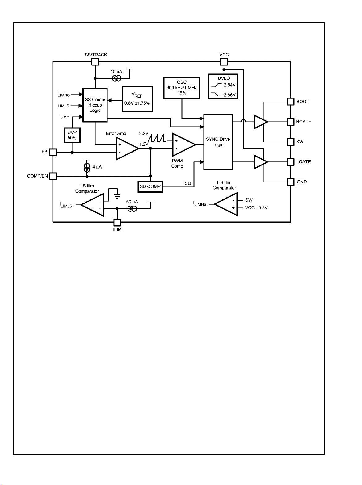
Block Diagram
LM3743
20177403
5 www.national.com
Page 6
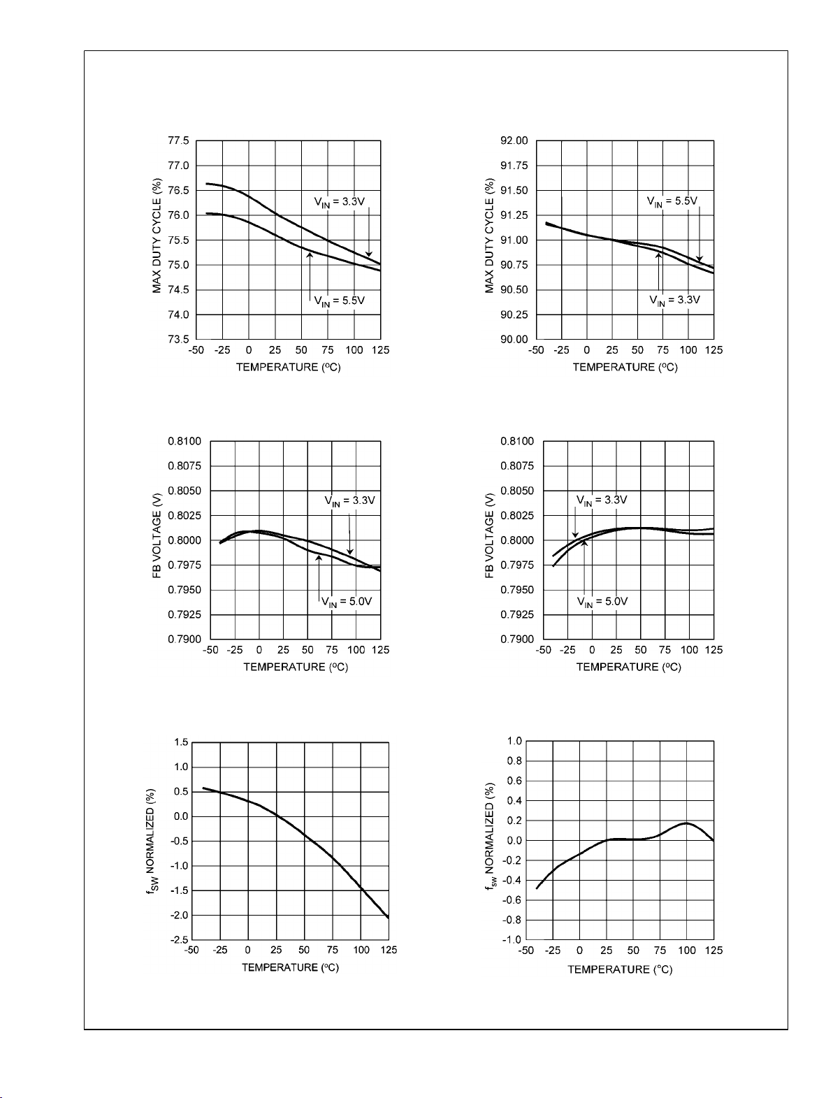
Typical Performance Characteristics V
= 3.3, TJ = 25°C, I
IN
= 1A unless otherwise specified.
LOAD
LM3743
D
vs Temperature
Max
fSW = 1 MHZ
FB vs Temperature
fSW = 1 MHZ
20177455
D
vs Temperature
Max
fSW = 300 kHz
FB vs Temperature
fSW = 300 kHz
20177456
20177457
Frequency vs Temperature
fSW = 1 MHz
20177459
www.national.com 6
20177458
Frequency vs Temperature
fSW = 300 kHz
201774a2
Page 7
LM3743
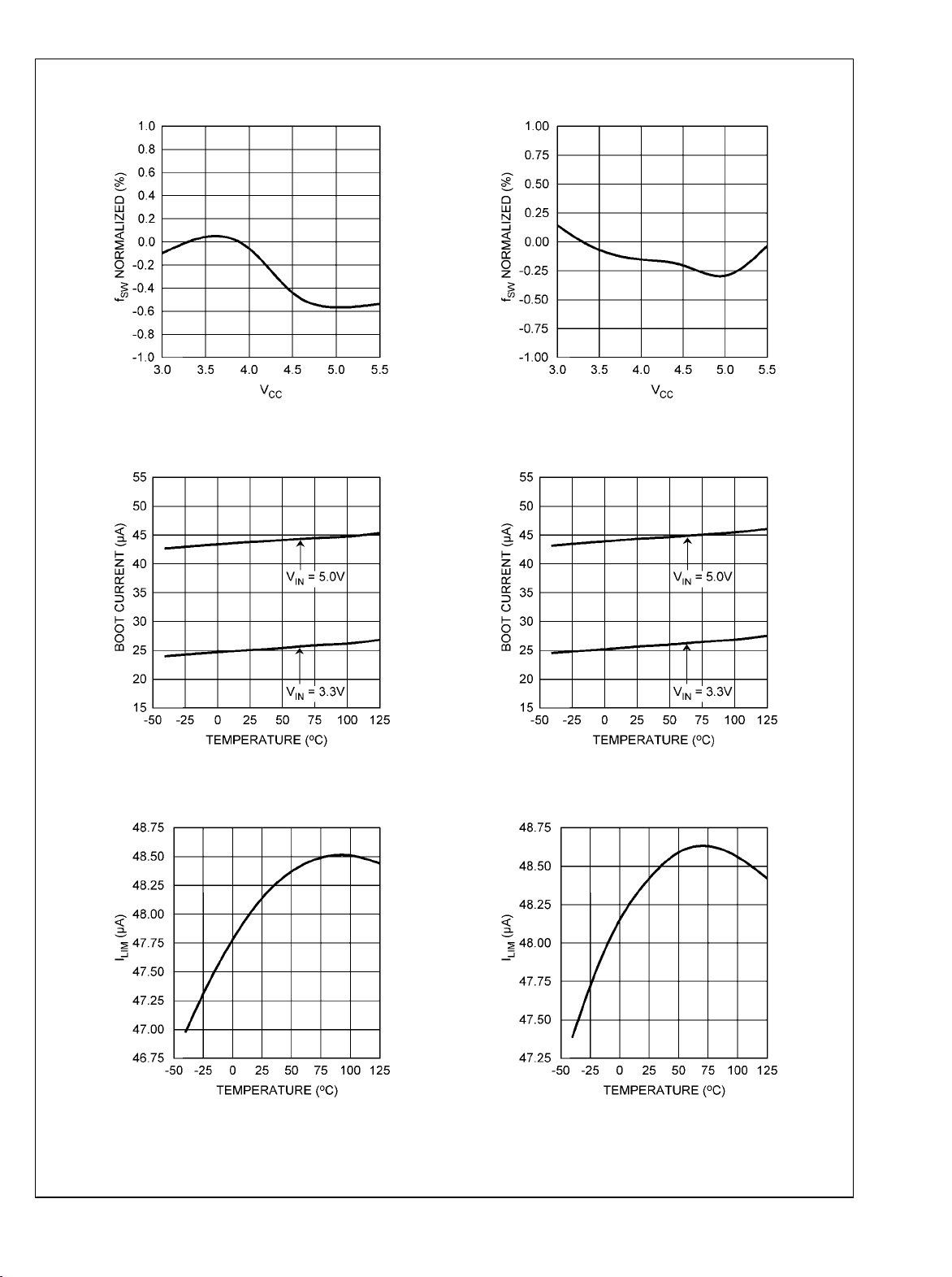
Frequency vs V
fSW = 1 MHz
I
SHDN_BOOT
fSW = 1 MHz
CC
vs Temperature
20177461
Frequency vs V
fSW = 300 kHz
I
SHDN_BOOT
fSW = 300 kHz
CC
20177462
vs Temperature
I
vs Temperature
LIM
fSW = 1 MHz
20177463
20177465
20177464
I
vs Temperature
LIM
fSW = 300 kHz
20177466
7 www.national.com
Page 8
LM3743
I
vs Temperature
VCC
fSW = 1 MHz
I
vs Temperature
VCC
fSW = 300 kHz
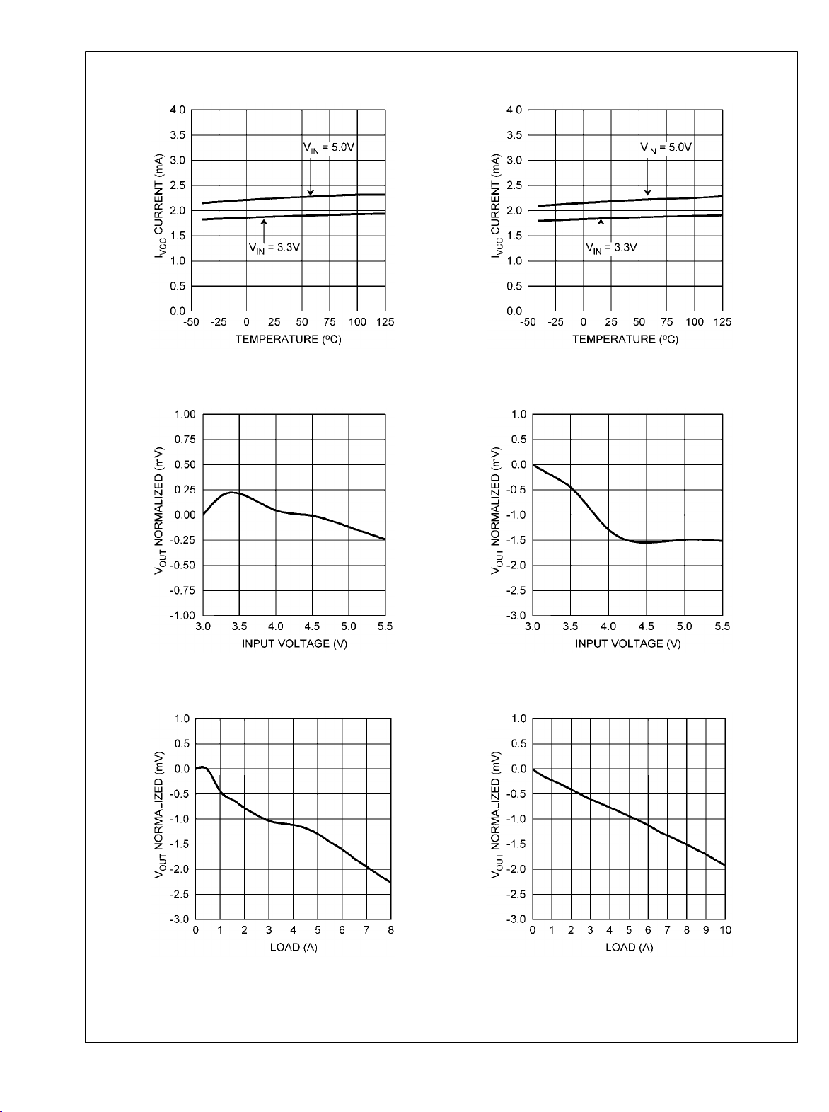
V
= 1.2V, I
OUT
OUT
Load Regulation
VIN = 3.3V, fSW = 1 MHz
Line Regulation
= 1A, fSW = 300 kHz
20177467
20177469
V
= 1.5V, I
OUT
= 1A, fSW = 1 MHz
OUT
Load Regulation
VIN = 3.3V, fSW = 300 kHz
Line Regulation
20177468
20177470
20177471
www.national.com 8
20177472
Page 9

LM3743
Efficiency vs Load
fSW = 1 MHz, V
Efficiency vs Load
fSW = 1 MHz, V
OUT
OUT
= 2.5V
= 1.5V
20177489
Efficiency vs Load
fSW = 1 MHz, V
Efficiency vs Load
fSW = 1 MHz, V
OUT
OUT
= 1.8V
20177488
= 1.2V
Efficiency vs Load
fSW = 1 MHz, V
OUT
= 1.0V
20177487
20177473
20177474
Efficiency vs Load
fSW = 1 MHz, V
9 www.national.com
OUT
= 0.8V
20177490
Page 10

LM3743
Efficiency vs Load
fSW = 300 kHz, V
OUT
= 2.5V
Efficiency vs Load
fSW = 300 kHz, V
OUT
= 1.8V
Efficiency vs Load
fSW = 300 kHz, V
Efficiency vs Load
fSW = 300 kHz, V
OUT
OUT
= 1.5V
= 1.0V
20177495
20177493
Efficiency vs Load
fSW = 300 kHz, V
Efficiency vs Load
fSW = 300 kHz, V
OUT
OUT
20177494
= 1.2V
20177492
= 0.8V
20177491
www.national.com 10
20177496
Page 11

LM3743
fSW = 1 MHz, VIN = 3.3V, I
Load Transient Response
(Refer to AN-1450 for BOM)
Shutdown
R
= 1Ω, VIN = 5V
LOAD
= 100 mA to 3.5A
LOAD
20177497
fSW = 300 kHz, VIN = 3.3V, I
Load Transient Response
(Refer to AN-1450 for BOM)
Pre Bias Startup
= 100 mA to 3.5A
LOAD
20177498
20177499
Application Information
THEORY OF OPERATION
The LM3743 is a voltage mode PWM buck controller featuring
synchronous rectification at 300 kHz or 1 MHz. In steady state
operation the LM3743 is always synchronous even at no load,
thus simplifying the compensation design. The LM3743 ensures a smooth and controlled start-up to support pre-biased
outputs. Two levels of current limit protection enhance the robustness of the power supply and requires no current sense
resistor in the power path. The primary level of protection is
the low side current limit and is achieved by sensing the voltage VDS across the low side MOSFET. The second level of
protection is the high side current limit, which protects power
components from extremely high currents, caused by switch
node short to ground.
NORMAL OPERATION
While in normal operation, the LM3743 IC controls the output
voltage by controlling the duty cycle of the power FETs. The
DC level of the output voltage is determined by a pair of feedback resistors using the following equation:
201774a0
(Designators refer to the Typical Application Circuit in the front
page)
For synchronous buck regulators, the duty ratio D is approximately equal to:
START UP
The LM3743 IC begins to operate when the COMP/EN pin is
released from a clamped condition and the voltage at the
VCC pin has exceeded 2.84V. Once these two conditions have
been met the internal 10µA current source begins to charge
the soft-start capacitor connected at the SS/TRACK pin. During soft-start the voltage on the soft-start capacitor is connected internally to the non-inverting input of the error
amplifier. The soft-start period lasts until the voltage on the
soft-start capacitor exceeds the LM3743 reference voltage of
0.8V. At this point the reference voltage takes over at the noninverting error amplifier input. The capacitance determines
the length of the soft-start period, and can be approximated
by:
C4 = (tSS x 10 µA) / 0.8V
11 www.national.com
Page 12

Where tSS is the desired soft-start time. In the event of either
VCC falling below UVLO or COMP/EN pin being pulled below
0.45V, the soft-start pin will discharge C4 to allow the output
LM3743
voltage to recover smoothly.
START UP WITH PRE-BIAS
A pre-bias output is a condition in which current from another
source has charged up the output capacitor of the switching
regulator before it has been turned on. The LM3743 features
a proprietary glitch free monotonic pre-bias start-up method
designed to ramp the output voltage from a pre-biased rail to
the target nominal output voltage. The IC limits the on time of
the low-side FET to 150 ns (typ) during soft-start, while allowing the high-side FET to adjust it's time according to softstart voltage, V
commutation of the load current is carried by the body diode
, and the internal voltage ramp. Any further
OUT
of the low-side FET or an external Schottky diode, if used. The
low side current limit is active during soft-start while allowing
the asynchronous switching. When soft-start is completed,
the on-time of the low-side FET is allowed to increase in a
controlled fashion up to the steady state duty cycle determined by the control loop. A plot of the LM3743 starting up
into a pre-biased condition is shown in the Typical Performance Characteristics section.
Note that the pre-bias voltage must not be greater than the
target output voltage of the LM3743, otherwise the LM3743
will pull the pre-bias supply down during steady state operation.
governing the values of the tracking divider resistors RT1 and
RT2 is:
The top resistance RT2 must be set to 1 kΩ in order to limit
current into the LM3743 during UVLO or shutdown. The final
voltage of the SS/TRACK pin should be slightly higher than
the feedback voltage of 0.8V, say about 0.85V as in the above
equation. The 50 mV difference will ensure the LM3743 to
reach regulation slightly before the master supply. If the master supply voltage was 5V and the LM3743 output voltage was
1.8V, for example, then the value of RT1 needed to give the
two supplies identical soft-start times would be 205Ω. A timing
diagram for the equal soft-start time case is shown in Figure
2.
TRACKING WITH EQUAL SOFT-START TIME
The LM3743 can track the output of a master power supply
during soft-start by connecting a resistor divider to the SS/
TRACK pin. In this way, the output voltage slew rate of the
LM3743 will be controlled by the master supply for loads that
require precise sequencing. When the tracking function is
used, no soft-start capacitor should be connected to the SS/
TRACK pin. However in all other cases, a capacitor value (C4)
of at least 560 pF should be connected between the soft-start
pin and ground.
20177430
20177431
FIGURE 2. Tracking with Equal Soft-Start Time
TRACKING WITH EQUAL SLEW RATES
The tracking feature can alternatively be used not to make
both rails reach regulation at the same time but rather to have
similar rise rates (in terms of output dV/dt). In this case, the
tracking resistors can be determined based on the following
equation:
For the example case of V
RT2 set to 1 kΩ as before, RT1 is calculated from the above
= 5V and V
OUT1
= 1.8V, with
OUT2
equation to be 887Ω. A timing diagram for the case of equal
slew rates is shown in Figure 3.
FIGURE 1. Tracking Circuit
One way to use the tracking feature is to design the tracking
resistor divider so that the master supply’s output voltage
(V
) and the LM3743’s output voltage (represented sym-
OUT1
bolically in Figure 1 as V
the power components) both rise together and reach their
, i.e. without explicitly showing
OUT2
target values at the same time. For this case, the equation
www.national.com 12
Page 13

20177433
FIGURE 3. Tracking with Equal Slew Rate
TRACKING AND SHUTDOWN SEQUENCING
LM3743 is designed to track the output of a master power
supply during start-up, but when the master supply powers
down the output capacitor of the LM3743 will discharge cycle
by cycle through the low-side FET. The off-time will reach
100% when the voltage at the track pin reaches zero volts.
This condition will persist as long as the master output voltage
is zero volts and the drivers of the LM3743 are still on. For
example if the load is required to not be discharged, the
drivers must be shut-off before the master powers down. This
is achieved by shutting down the LM3743 or bring VCC below
UVLO falling threshold. In this case the load will not be discharged.
SHUTDOWN
The LM3743 IC can be put into shutdown mode by bringing
the voltage at the COMP/EN pin below 0.45V (typ). The quiescent current during shutdown is approximately 6 µA (typ).
During shutdown both the high-side and low-side FETs are
disabled. The soft-start capacitor is discharged through an
internal FET so that the output voltage rises in a controlled
fashion when the part is enabled again. When enabled a 4 µA
pull-up current increases the charge of the compensation capacitors.
UNDER VOLTAGE LOCK-OUT (UVLO)
If VCC drops below 2.66V (typ), the chip enters UVLO mode.
UVLO consists of turning off the top and bottom FETs and
remaining in that condition until VCC rises above 2.84V (typ).
As with shutdown, the soft-start capacitor is discharged
through an internal FET, ensuring that the next start-up will
be controlled by the soft-start circuitry.
MOSFET GATE DRIVE
The LM3743 has two gate drivers designed for driving Nchannel MOSFETs in synchronous mode. Power for the high
gate driver is supplied through the BOOT pin, while driving
power for the low gate is provided through the VCC pin. The
BOOT voltage is supplied from a local charge pump structure
which consists of a Schottky diode and 0.1 µF capacitor,
shown in Figure 4. Since the bootstrap capacitor (C10) is
connected to the SW node, the peak voltage impressed on
the BOOT pin is the sum of the input voltage (VIN) plus the
voltage across the bootstrap capacitor (ignoring any forward
drop across the bootstrap diode). The bootstrap capacitor is
charged up by VIN (called V
MOSFET turns off.
here) whenever the upper
BOOT_DC
20177434
FIGURE 4. Charge Pump Circuit and Driver Circuitry
The output of the low-side driver swings between VCC and
ground, whereas the output of the high-side driver swings between VIN + V
FET fully on, the Gate pin voltage of the MOSFET must be
and VIN. To keep the high-side MOS-
BOOT_DC
higher than its instantaneous Source pin voltage by an
amount equal to the 'Miller plateau'. It can be shown that this
plateau is equal to the threshold voltage of the chosen MOSFET plus a small amount equal to I
maximum load current of the application, and g is the
/g. Here I
OUT
OUT
is the
transconductance of this MOSFET (typically about 100 for
logic-level devices). That means we must choose V
to at least exceed the Miller plateau level. This may therefore
BOOT_DC
affect the choice of the threshold voltage of the external MOSFETs, and that in turn may depend on the chosen VIN rail.
So far in the discussion above, the forward drop across the
bootstrap diode has been ignored. But since that does affect
the output of the driver, it is a good idea to include this drop
in the following examples. Looking at the Typical Application
schematic, this means that the difference voltage VIN - VD1,
which is the voltage the bootstrap capacitor charges up to,
must always be greater than the maximum tolerance limit of
the threshold voltage of the upper MOSFET. Here VD1 is the
forward voltage drop across the bootstrap diode D1. This
voltage drop may place restrictions on the type of MOSFET
selected.
The capacitor C10 serves to maintain enough voltage between the top MOSFET gate and source to control the device
even when the top MOSFET is on and its source has risen up
to the input voltage level. The charge pump circuitry is fed
from VIN, which can operate over a range from 3.0V to 5.5V.
Using this basic method the voltage applied to the high side
gate VIN - VD1. This method works well when VIN is 5V±10%,
because the gate drives will get at least 4.0V of drive voltage
during the worst case of V
Logic level MOSFETs generally specify their on-resistance at
= 4.5V and V
IN-MIN
D1-MAX
= 0.5V.
VGS = 4.5V. When VCC = 3.3V±10%, the gate drive at worst
case could go as low as 2.5V. Logic level MOSFETs are not
guaranteed to turn on, or may have much higher on-resistance at 2.5V. Sub-logic level MOSFETs, usually specified at
VGS = 2.5V, will work, but are more expensive and tend to
have higher on-resistance.
LM3743
13 www.national.com
Page 14

LOW-SIDE CURRENT LIMIT
The main current limit of the LM3743 is realized by sensing
LM3743
the voltage drop across the low-side FET as the load current
passes through it. The R
ue; hence the voltage across the MOSFET can be determined
of the MOSFET is a known val-
DSON
as:
VDS = I
OUT
x R
DSON
The current flowing through the low-side MOSFET while it is
on is the falling portion of the inductor current. The current
limit threshold is determined by an external resistor, R1, connected between the switching node and the ILIM pin. A constant current (I
causing a fixed voltage drop. This fixed voltage is compared
) of 50 µA typical is forced through R1,
ILIM
against VDS and if the latter is higher, the current limit of the
chip has been reached. To obtain a more accurate value for
R1 you must consider the operating values of R
I
at their operating temperatures in your application and
ILIM
the effect of slight parameter variations from part to part. R1
can be found by using the following equation using the
R
value of the low side MOSFET at it's expected hot
DSON
temperature and the absolute minimum value expected over
the full temperature range for the I
which is 42.5 µA:
ILIM
R1 = R
DSON-HOT
x I
CLIM
/ I
ILIM
For example, a conservative 15A current limit (I
design with a R
resistor. The LM3743 enters current limit mode if the inductor
DSON-HOT
of 10 mΩ would require a 3.83 kΩ
current exceeds the set current limit threshold. The inductor
current is first sampled 50 ns after the low-side MOSFET turns
on. Note that in normal operation mode the high-side MOSFET always turns on at the beginning of a clock cycle. In
current limit mode, by contrast, the high-side MOSFET onpulse is skipped. This causes inductor current to fall. Unlike
a normal operation switching cycle, however, in a current limit
mode switching cycle the high-side MOSFET will turn on as
soon as inductor current has fallen to the current limit threshold.
CLIM
and
DSON
) in a 10A
normally well defined, but the peaks are variable, according
to the duty cycle, see Figure 5. The PWM error amplifier and
comparator control the pulse of the high-side MOSFET, even
during current limit mode, meaning that peak inductor current
can exceed the current limit threshold. For example, during
an output short-circuit to ground, and assuming that the output inductor does not saturate, the maximum peak inductor
current during current limit mode can be calculated with the
following equation:
Where TSW is the inverse of switching frequency fSW. The 200
ns term represents the minimum off-time of the duty cycle,
which ensures enough time for correct operation of the current sensing circuitry.
In order to minimize the temperature effects of the peak inductor currents, the IC enters hiccup mode after 15 over
current events, or a long current limit event that lasts 15
switching cycles (the counter is reset when 32 non-current
limit cycles occur in between two current limit events). Hiccup
mode will be discussed in further detail in the “Hiccup Mode
and Internal Soft-Start” section.
HIGH-SIDE COARSE CURRENT LIMIT
The LM3743 employs a comparator to monitor the voltage
across the high-side MOSFET when it is on. This provides
protection for short circuits from switch node to ground or the
case when the inductor is shorted, which the low side current
limit cannot detect. A 200 ns blanking time period after the
high-side FET turns on is used to prevent switching transient
voltages from tripping the high-side current limit without
cause. If the difference between VCC pin and SW pin voltage
exceeds 500 mV, the LM3743 will immediately enter hiccup
mode (see Hiccup Mode section).
OUTPUT UNDER-VOLTAGE PROTECTION (UVP)
After the end of soft-start the output UVP comparator is activated. The threshold is 50% of the feedback voltage. Once
the comparator indicates UVP for more than 7 µs typ. (glitch
filter time), the IC goes into hiccup mode.
20177444
FIGURE 5. Current Limit Threshold
The low-side current sensing scheme can only limit the current during the converter off-time, when inductor current is
falling. Therefore in a typical current limit plot the valleys are
www.national.com 14
HICCUP MODE AND INTERNAL SOFT-START
Hiccup protection mode is designed to protect the external
components of the circuit (output inductor, FETs, and input
voltage source) from thermal stress. During hiccup mode, the
LM3743 disables both the high-side and low-side FETs and
begins a cool down period of 5.5 ms. At the conclusion of this
cool down period, the regulator performs an internal 3.6 ms
soft-start. There are three distinct conditions under which the
IC will enter the hiccup protection mode:
1.
The low-side current sensing threshold has exceeded
the current limit threshold for fifteen sampled cycles, see
Figure 6. Each cycle is sampled at the start of each off
time (t
when 32 consecutive non-current limit cycles occur in
). The low-side current limit counter is reset
OFF
between two current limit events.
2.
The high-side current limit comparator has sensed a
differential voltage larger than 500 mV.
3.
The voltage at the FB pin has fallen below 0.4V, and the
UVP comparator has sensed this condition for 7 μs
(during steady state operation).
The band gap reference, the external soft-start, and internal
hiccup soft-start of 3.6 ms (typ) connect to the non-inverting
Page 15

LM3743
input of the error amplifier through a multiplexer. The lowest
voltage of the three connects directly to the non-inverting input. Hiccup mode will not discharge the external soft-start,
only UVLO or shut-down will. When in hiccup mode the internal 5.5 ms timer is set, and the internal soft-start capacitor is
discharged. After the 5.5 ms timeout, the internal 3.6 ms softstart begins, see Figure 7. During soft-start, only low-side
current limit and high side current limit can put the LM3743
into hiccup mode.
20177452
FIGURE 6. Entering Hiccup Mode
DESIGN CONSIDERATIONS
The following is a design procedure for selecting all the components in the Typical Application circuit on the front page.
This design converts 5V (VIN) to 1.8V (V
load of 10A with an efficiency of 90% and a switching fre-
) at a maximum
OUT
quency of 300 kHz. The same procedures can be followed to
create many other designs with varying input voltages, output
voltages, load currents, and switching frequency.
Switching Frequency
Selection of the operating switching frequency is based on
trade-offs between size, cost, efficiency, and response time.
For example, a lower frequency will require larger more expensive inductors and capacitors. While a higher switching
frequency will generally reduce the size of these components,
but will have a reduction in efficiency. Fast switching converters allow for higher loop gain bandwidths, which in turn have
the ability to respond quickly to load and line transients. For
the example application we have chosen a 300 kHz switching
frequency because it will reduce the switching power losses
and in turn allow for higher conduction losses considering the
same power loss criteria, thus it is possible to sustain a higher
load current.
Output Inductor
The output inductor is responsible for smoothing the square
wave created by the switching action and for controlling the
output current ripple (ΔI
the inductor current. The DC current into the load is equal to
) also called the AC component of
OUT
the average current flowing in the inductor. The inductance is
chosen by selecting between trade-offs in efficiency, size, and
response time. The recommended percentage of AC component to DC current is 30% to 40%, this will provide the best
trade-off between energy requirements and size, (read
AN-1197 for theoretical analysis). Another criteria is the ability
to respond to large load transient responses; the smaller the
output inductor, the more quickly the converter can respond.
The equation for output inductor selection is:
20177406
FIGURE 7. Hiccup Time-Out and Internal Soft-Start
For example, if the low-side current limit is 10A, then once in
overload the low-side current limit controls the valley current
and only allows an average amount of 10A plus the ripple
current to pass through the inductor and FETs for 15 switching
cycles. In such an amount of time, the temperature rise is very
small. Once in hiccup mode, the average current through the
high-side FET is:
I
= (I
HSF-AVE
+ ΔI) x [ D(15 cycles x TSW) ] / 5.5 ms
CLIM
equals 71 mA. With an arbitrary D = 60%, ripple current of 3A,
and a 300 kHz switching frequency.
The average current through the low-side FET is:
I
= (I
LSF-AVE
+ ΔI) x [ (1–D) x (15 cycles x TSW) ] / 5.5 ms
CLIM
equals 47 mA,
And the average current through the inductor is:
I
= (I
L-AVE
+ ΔI) x [ (15 cycles x TSW) ] / 5.5 ms
CLIM
equals 118 mA.
Here we have plugged in the values for input voltage, output
voltage, switching frequency, and 30% of the maximum load
current. This yields an inductance of 1.34 µH. The output inductor must be rated to handle the peak current (also equal
to the peak switch current), which is (I
11.5A, for a 10A design and a AC current of 3A.
+ (0.5 x ΔI
OUT
OUT
)) =
The Coiltronics DR125–1R5 is 1.5 µH, is rated to 13.8A RMS
current, and has a direct current resistance (DCR) of 3 mΩ.
After selecting the Coiltronics DR125–1R5 for the output inductor, actual inductor current ripple must be re-calculated
with the selected inductance value. This information is needed to determine the RMS current through the input and output
capacitors. Re-arranging the equation used to select inductance yields the following:
15 www.national.com
Page 16

LM3743
V
is assumed to be 10% above the steady state input
IN(MAX)
voltage, or 5.5V at VIN = 5.0V. The re-calculated current ripple
will then be 2.69A. This gives a peak inductor/switch current
will be 11.35A.
Output Capacitor
The output capacitor in a switching regulator is selected on
the basis of capacitance, equivalent series resistance (ESR),
size, and cost. In this example the output current is 10A and
the expected type of capacitor is an aluminum electrolytic, as
with the input capacitors. An important specification in switching converters is the output voltage ripple ΔV
the impedance of most capacitors is very small compared to
ESR, hence ESR becomes the main selection criteria. In this
design the load requires a 2% ripple , which results in a
ΔV
of 36 mV
OUT
ESR
(Ta), solid aluminum, organic, and niobium (Nb) capacitors
is 13 mΩ. Aluminum electrolytic (Al-E), tantalum
MAX
. Thus the maximum ESR is then:
P-P
are all popular in switching converters. In general, by the time
enough capacitors have been paralleled to obtain the desired
ESR, the bulk capacitance is more than enough to supply the
load current during a transient from no-load to full load. The
number and type of capacitors used depends mainly on their
size and cost. One exception to this is multi-layer ceramic capacitors. MLCCs have very low ESR, but also low capacitance in comparison with other types. This makes them
attractive for lower power designs. For higher power or for fast
load transients the number of MLCCs needed often increases
the size and cost to unacceptable levels. Because the load
could transition quickly from 0 to 10A, more bulk capacitance
is needed than the MLCCs can provide. One compromise is
a solid electrolytic POSCAP from Sanyo or SP-caps from
Panasonic. POSCAP and SPcaps often have large capacitances needed to supply currents for load transients, and low
ESRs. The 6TPD470M by Sanyo has 470 µF, and a maximum
ESR of 10 mΩ. Solid electrolytics have stable ESR relative to
temperature, and capacitance change is relatively immune to
bias voltage. Tantalums (Ta), niobium (Nb), and Al-E are
good solutions for ambient operating temperatures above 0°
C, however their ESR tends to increase quickly below 0°C
ambient operating temperature, so these capacitor types are
not recommended for this area of operation.
Input Capacitor
The input capacitors in a buck converter are subjected to high
RMS current stress. Input capacitors are selected for their
ability to withstand the heat generated by the RMS current
and the ESR as specified by the manufacturer. Input RMS
ripple current is approximately:
Where duty cycle D = V
buck converter occurs during full load and when the duty cycle
. The worst-case ripple for a
OUT/VIN
(D) is 0.5.
OUT
. At 300 kHz
When multiple capacitors of the same type and value are paralleled, the power dissipated by each input capacitor is:
where n is the number of paralleled capacitors, and ESR is
the equivalent series resistance of each capacitor. The equation above indicates that power loss in each capacitor decreases rapidly as the number of input capacitors increases.
For this 5V to 1.8V design the duty cycle is 0.36. For a 10A
maximum load the RMS current is 4.8A.
Connect one or two 22 µF MLCC as close as possible across
the drain of the high-side MOSFET and the source of the lowside MOSFET, this will provide high frequency decoupling
and satisfy the RMS stress. A bulk capacitor is recommended
in parallel with the MLCC in order to prevent switching frequency noise from reflecting back into the input line, this
capacitor should be no more than 1inch away from the MLCC
capacitors.
MOSFETs
Selection of the power MOSFETs is governed by a trade-off
between cost, size, and efficiency. One method is to determine the maximum cost that can be endured, and then select
the most efficient device that fits that price. Using a spreadsheet to estimate the losses in the high-side and low-side
MOSFETs is one way to determine relative efficiencies between different MOSFETs. Good correlation between the
prediction and the bench result is not guaranteed.
Losses in the high-side MOSFET can be broken down into
conduction loss, gate charging loss, and switching loss. Conduction, or I2R loss, is approximately:
For the high side FET:
PC = D (I
OUT
x R
DSON-HI
x 1.3)
2
For the low side FET:
PC = (1 - D) x (I
OUT
x R
DSON-LO
x 1.3)
2
In the above equations the factor 1.3 accounts for the increase in MOSFET R
1.3 can be ignored and the R
using the R
manufacturer datasheet.
vs. Temperature curves in the MOSFET
DSON
due to heating. Alternatively, the
DSON
of the MOSFET estimated
DSON
Gate charging loss results from the current driving the gate
capacitance of the power MOSFETs, and is approximated as:
PGC = (VCC) x QG x f
SW
VCC is the driving voltage (see MOSFET Gate Driver section)
and QG is the gate charge of the MOSFET. If multiple devices
will be placed in parallel, their gate charges can simply be
summed to form a cumulative QG.
Switching loss occurs during the brief transition period as the
high-side MOSFET turns on and off, during which both current
and voltage are present in the channel of the MOSFET. It can
be approximated as:
PSW = 0.5 x VIN x I
x (tr + tf) x f
OUT
SW
where tr and tf are the rise and fall times of the MOSFET.
Switching loss occurs in the high-side MOSFET only.
For this example, the maximum drain-to-source voltage applied to either MOSFET is 5.5V. The maximum drive voltage
at the gate of the high-side MOSFET is 5.0V, and the maximum drive voltage for the low-side MOSFET is 5.5V. For
www.national.com 16
Page 17

designs between 5A and 10A, single MOSFETs in SO-8 provide a good trade-off between size, cost, and efficiency.
VCC Filtering
To ensure smooth DC voltage for the chip supply a 1 µF (C3),
X5R MLCC type or better must be placed as close as possible
to the VCC and GND pin. Together with a small 1 to 4.99Ω
resistor placed between the input rail and the VCC pin, a low
pass filter is formed to filter out high frequency noise from
injecting into the VCC rail. Since VCC is also the sense pin for
the high-side current limit, the resistor should connect close
to the drain of the high-side MOSFET to prevent IR drops due
to trace resistance. A second design consideration is the low
pass filter formed by C3 and R6 on the VCC pin, a fast slew
rate, large amplitude load transient may cause a larger voltage droop on CIN than on VCC pin. This may lead to a lower
current at which high-side protection may occur. Thus increase the bulk input capacitor if the high-side current limit is
engaging due to a dynamic load transient behavior as explained above.
Bootstrap Diode (D1)
The MBR0520 and BAT54 work well as a bootstrap diode in
most designs. Schottky diodes are the preferred choice for
the bootstrap circuit because of their low forward voltage
drop. For circuits that will operate at high ambient temperature
the Schottky diode datasheet must be read carefully to ensure
that the reverse current leakage at high temperature does not
increase enough to deplete the charge on the bootstrap capacitor while the high side FET is on. Some Schottky diodes
increase their reverse leakage by as much as 1000 times at
high temperatures. Fast rectifier and PN junction diodes
maintain low reverse leakage even at high ambient temperature. These diode types have higher forward voltage drop but
can still be used for high ambient temperature operation.
Control Loop Compensation
The LM3743 uses voltage-mode (‘VM’) PWM control to correct changes in output voltage due to line and load transients.
VM requires careful small signal compensation of the control
loop for achieving high bandwidth and good phase margin.
The control loop is comprised of two parts. The first is the
power stage, which consists of the duty cycle modulator, output inductor, output capacitor, and load. The second part is
the error amplifier, which for the LM3743 is a 30 MHz op-amp
used in the classic inverting configuration. Figure 8 shows the
regulator and control loop components.
20177413
FIGURE 8. Power Stage and Error Amp
One popular method for selecting the compensation components is to create Bode plots of gain and phase for the power
stage and error amplifier. Combined, they make the overall
bandwidth and phase margin of the regulator easy to see.
Software tools such as Excel, MathCAD, and Matlab are useful for showing how changes in compensation or the power
stage affect system gain and phase.
The power stage modulator provides a DC gain ADC that is
equal to the input voltage divided by the peak-to-peak value
of the PWM ramp. This ramp is 1.0V
inductor and output capacitor create a double pole at fre-
for the LM3743. The
pk-pk
quency fDP, and the capacitor ESR and capacitance create a
single zero at frequency f
5.0V, these quantities are:
. For this example, with VIN =
ESR
LM3743
In the equation for fDP, the variable RL is the power stage resistance, and represents the inductor DCR plus the on resistance of the top power MOSFET. RO is the output voltage
divided by output current. The power stage transfer function
GPS is given by the following equation, and Figure 9 shows
Bode plots of the phase and gain in this example.
a = LCO(RO + RC)
17 www.national.com
Page 18

b = L + CO(RORL + RORC + RCRL)
c = RO + R
LM3743
L
20177418
of the switching frequency, or 60 kHz for this example. The
generic equation for the error amplifier transfer function is:
In this equation the variable AEA is a ratio of the values of the
capacitance and resistance of the compensation components, arranged as shown in Figure 8. AEA is selected to
provide the desired bandwidth. A starting value of 80,000 for
AEA should give a conservative bandwidth. Increasing the
value will increase the bandwidth, but will also decrease
phase margin. Designs with 45-60° are usually best because
they represent a good trade-off between bandwidth and
phase margin. In general, phase margin is lowest and gain
highest (worst-case) for maximum input voltage and minimum
output current. One method to select AEA is to use an iterative
process beginning with these worst-case conditions.
1.
Increase A
2.
Check overall bandwidth and phase margin
3.
Change VIN to minimum and recheck overall bandwidth
EA
and phase margin
4.
Change IO to maximum and recheck overall bandwidth
and phase margin
The process ends when both bandwidth and phase margin
are sufficiently high. For this example input voltage can vary
from 4.5V to 5.5V and output current can vary from 0 to 10A,
and after a few iterations a moderate gain factor of 90 dB is
used.
The error amplifier of the LM3743 has a unity-gain bandwidth
of 30 MHz. In order to model the effect of this limitation, the
open-loop gain can be calculated as:
20177419
FIGURE 9. Power Stage Gain and Phase
The double pole at 6 kHz causes the phase to drop to approximately -140° at around 15 kHz. The ESR zero, at 33.9
kHz, provides a +90° boost that prevents the phase from
dropping to -180º. If this loop were left uncompensated, the
bandwidth would be approximately 15 kHz and the phase
margin 40°. In theory, the loop would be stable, but would
suffer from poor DC regulation (due to the low DC gain) and
would be slow to respond to load transients (due to the low
bandwidth.) In practice, the loop could easily become unstable due to tolerances in the output inductor, capacitor, or
changes in output current, or input voltage. Therefore, the
loop is compensated using the error amplifier and a few passive components.
For this example, a Type III, or three-pole-two-zero approach
gives optimal bandwidth and phase.
In most voltage mode compensation schemes, including
Type III, a single pole is placed at the origin to boost DC gain
as high as possible. Two zeroes fZ1 and fZ2 are placed at the
double pole frequency to cancel the double pole phase lag.
Then, a pole, fP1 is placed at the frequency of the ESR zero.
A final pole fP2 is placed at one-half of the switching frequency.
The gain of the error amplifier transfer function is selected to
give the best bandwidth possible without violating the Nyquist
stability criteria. In practice, a good crossover point is one-fifth
The new error amplifier transfer function that takes into account unity-gain bandwidth is:
The gain and phase of the error amplifier are shown in Figure
10.
www.national.com 18
Page 19

20177423
20177424
FIGURE 10. Error Amp. Gain and Phase
In VM regulators, the top feedback resistor R2 forms a part of
the compensation. Setting R2 to 10 kΩ±1%, usually gives
values for the other compensation resistors and capacitors
that fall within a reasonable range. (Capacitances > 1 pF, resistances <1 MΩ) C7, C8, C9, R4, and R5 are selected to
provide the poles and zeroes at the desired frequencies, using the following equations:
LM3743
In practice, a good trade off between phase margin and bandwidth can be obtained by selecting the closest ±10% capacitor values above what are suggested for C7 and C8, the
closest ±10% capacitor value below the suggestion for C9,
and the closest ±1% resistor values below the suggestions
for R4, R5. Note that if the suggested value for R5 is less than
100Ω, it should be replaced by a short circuit. Following this
guideline, the compensation components will be:
C7 = 47 pF±10%, C9 = 1.5 nF±10%
C8 = 2.2 nF±10%, R4 = 22.6 kΩ±1%
R5 = 2.1 kΩ±1%
The transfer function of the compensation block can be de-
rived by considering the compensation components as
impedance blocks ZF and ZI around an inverting op-amp:
As with the generic equation, G
take into account the limited bandwidth of the error amplifier.
EA-ACTUAL
must be modified to
The result is:
19 www.national.com
Page 20

The total control loop transfer function H is equal to the power
stage transfer function multiplied by the error amplifier transfer function.
LM3743
H = GPS x H
EA
The bandwidth and phase margin can be read graphically
from Bode plots of HEA as shown in Figure 11.
FIGURE 11. Overall Loop Gain and Phase
The bandwidth of this example circuit is 59 kHz, with a phase
margin of 60°.
EFFICIENCY CALCULATIONS
The following is a sample calculation.
A reasonable estimation of the efficiency of a switching buck
controller can be obtained by adding together the Output
Power (P
) loss and the Total Power loss (P
OUT
20177429
20177450
LOSS
FET Switching Loss (PSW)
PSW = P
PSW = 0.5 x VIN x I
SW(ON)
+ P
SW(OFF)
x (tr + tf) x f
OUT
SW
PSW = 0.5 x 5V x 10A x 300 kHz x 67 ns
PSW = 503 mW
The Si4866DY has a typical turn-on rise time tr and turn-off
fall time tf of 32 ns and 35 ns, respectively. The switching
losses for the upper FET (Q1) is 0.503W. The low side FET
(Q2) does not incur switching losses.
FET Conduction Loss (P
P
CND
P
= I
CND1
P
= I
CND2
R
= 4.5 mΩ and the k factor accounts for the increase
DS(ON)
in R
due to heating. k = 1.3 at TJ = 100°C
DS(ON)
P
= (10A)2 x 4.5 mΩ x 1.3 x 0.36
CND1
P
= (10A)2 x 4.5 mΩ x 1.3 x (1 - 0.36)
CND2
P
CND
P
= 211 mW + 374 mW = 585 mW
CND
FET Gate Charging Loss (P
P
= n x ( VCC - VD1 ) x QGS x f
GATE_H
P
GATE_L
P
= [ 1 x ( 5.0V - 0.4V ) x 22 nC x 300 kHz ] + [ 1 x ( 5.0V )
GATES
P
x 22 nC x 300 kHz ]
= 29 mW + 33 mW = 62 mW
GATES
)
CND
2
= P
2
OUT
= P
OUT
CND1
x R
x R
CND1
DS(ON)
GATE
+ P
CND2
DS(ON)
x k x (1-D)
+ P
CND2
)
x k x D
= n x VCC x QGS x f
SW
SW
The value n is the total number of FETs used and QGS is the
typical gate-source charge value, which is 21 nC. For the
Si4866DY the gate charging loss is 62 mW.
Thus the total MOSFET losses are:
P
= PSW + P
FET
CND
+ P
GATES
=
503 mW + 585 mW + 62 mW
P
= 1.15 W
FET
There are few additional losses that are taken into account:
IC Loss (PIC)
POP = I
PDR = [[ (n x QGS x fSW) / D] +[ (n x QGS x fSW) / (1–D) ]] x V
where POP is the operating loss, PDR is the driver loss, I
is the typical operating VCC current
VCC
Q_VCC
x V
CC
CC
Q-
POP= ( 1.3 mA x 5.0V )
PDR= [( 1 x 22 nC x 300 kHz ) / .36 ] + [( 1 x 22 nC x 300
kHz ) / .64 ] x V
):
PIC= POP + P
CC
DR
PIC= 6.5 mW + 137 mW = 143.5 mW
Input Capacitor Loss (P
CAP
)
The Output Power (P
design is (1.8V x 10A) = 18W. The Total Power (P
an efficiency calculation to complement the design, is shown
) for the Typical Application Circuit
OUT
LOSS
), with
below.
The majority of the power losses are due to the low side and
high side MOSFET’s losses. The losses in any MOSFET are
switching (PSW), conduction losses (P
losses (P
www.national.com 20
GATE
)
), and gate charging
CND
where,
Page 21

LM3743
Here n is the number of paralleled capacitors, ESR is the
equivalent series resistance of each, and P
tion in each. So for example if we use only one input capacitor
is the dissipa-
CAP
of 10mΩ.
P
= 230 mW
CAP
Output Inductor Loss (P
P
IND
IND
= I
2
)
OUT
x DCR
where DCR is the DC resistance. Therefore, for example
P
= (10A)2 x 3 mΩ
IND
P
= 302 mW
IND
Total System Efficiency
P
= P
LOSS
+ PIC + P
FET
CAP
+ P
IND
PCB LAYOUT CONSIDERATIONS
To produce an optimal power solution with the LM3743, good
layout and design of the PCB are as important as component
selection. The following are several guidelines to aid in creating a good layout. For an extensive PCB layout explanation
refer to AN-1229.
Separate Power Ground and Signal Ground
Good layout techniques include a dedicated ground plane,
preferably on an internal layer. Signal level components like
the compensation and feedback resistors should be connected to a section of this internal plane, signal ground. The signal
ground section of the plane should be connected to the power
ground at a single point. The best place to connect the signal
ground and power ground is right at the GND pin of the IC.
Low Impedance Power Path
The power path includes the input capacitors, power FETs,
output inductor, and output capacitors. Keep these components on the same side of the PCB and connect them with
thick traces or copper planes on the same layer. Vias add
resistance and inductance to the power path, and have high
impedance connections to internal planes than do top or bottom layers of a PCB. If heavy switching currents must be
routed through vias and/or internal planes, use multiple vias
in parallel to reduce their resistance and inductance. The
power components must be kept close together. The longer
the paths that connect them, the more they act as antennas,
radiating unwanted EMI.
Minimize the Switch Node Copper
The plane that connects the power FETs and output inductor
together radiates more EMI as it gets larger. Use just enough
copper to give low impedance to the switching currents.
Kelvin Traces For Sense Lines
The drain and the source of the high-side FET should be connected as close as possible to the VCC filter resistor (R6) and
the SW pin and each pin should connect with a separate trace.
The feedback trace should connect the positive node of the
output capacitor and connect to the top feedback resistor
(R2). Keep this trace away from the switch node and from the
output inductor. If driving the COMP pin low with a signal BJT
or MOSFET make sure to keep the signal transistor as close
as possible to the pin and keep the trace away from EMI radiating nodes and components.
21 www.national.com
Page 22

Physical Dimensions inches (millimeters) unless otherwise noted
LM3743
MSOP-10 Pin Package
NS Package Number MUB10A
www.national.com 22
Page 23

Notes
LM3743
23 www.national.com
Page 24

Notes
THE CONTENTS OF THIS DOCUMENT ARE PROVIDED IN CONNECTION WITH NATIONAL SEMICONDUCTOR CORPORATION
(“NATIONAL”) PRODUCTS. NATIONAL MAKES NO REPRESENTATIONS OR WARRANTIES WITH RESPECT TO THE ACCURACY
OR COMPLETENESS OF THE CONTENTS OF THIS PUBLICATION AND RESERVES THE RIGHT TO MAKE CHANGES TO
SPECIFICATIONS AND PRODUCT DESCRIPTIONS AT ANY TIME WITHOUT NOTICE. NO LICENSE, WHETHER EXPRESS,
IMPLIED, ARISING BY ESTOPPEL OR OTHERWISE, TO ANY INTELLECTUAL PROPERTY RIGHTS IS GRANTED BY THIS
DOCUMENT.
TESTING AND OTHER QUALITY CONTROLS ARE USED TO THE EXTENT NATIONAL DEEMS NECESSARY TO SUPPORT
NATIONAL’S PRODUCT WARRANTY. EXCEPT WHERE MANDATED BY GOVERNMENT REQUIREMENTS, TESTING OF ALL
PARAMETERS OF EACH PRODUCT IS NOT NECESSARILY PERFORMED. NATIONAL ASSUMES NO LIABILITY FOR
APPLICATIONS ASSISTANCE OR BUYER PRODUCT DESIGN. BUYERS ARE RESPONSIBLE FOR THEIR PRODUCTS AND
APPLICATIONS USING NATIONAL COMPONENTS. PRIOR TO USING OR DISTRIBUTING ANY PRODUCTS THAT INCLUDE
NATIONAL COMPONENTS, BUYERS SHOULD PROVIDE ADEQUATE DESIGN, TESTING AND OPERATING SAFEGUARDS.
EXCEPT AS PROVIDED IN NATIONAL’S TERMS AND CONDITIONS OF SALE FOR SUCH PRODUCTS, NATIONAL ASSUMES NO
LIABILITY WHATSOEVER, AND NATIONAL DISCLAIMS ANY EXPRESS OR IMPLIED WARRANTY RELATING TO THE SALE
AND/OR USE OF NATIONAL PRODUCTS INCLUDING LIABILITY OR WARRANTIES RELATING TO FITNESS FOR A PARTICULAR
PURPOSE, MERCHANTABILITY, OR INFRINGEMENT OF ANY PATENT, COPYRIGHT OR OTHER INTELLECTUAL PROPERTY
RIGHT.
LIFE SUPPORT POLICY
NATIONAL’S PRODUCTS ARE NOT AUTHORIZED FOR USE AS CRITICAL COMPONENTS IN LIFE SUPPORT DEVICES OR
SYSTEMS WITHOUT THE EXPRESS PRIOR WRITTEN APPROVAL OF THE CHIEF EXECUTIVE OFFICER AND GENERAL
COUNSEL OF NATIONAL SEMICONDUCTOR CORPORATION. As used herein:
Life support devices or systems are devices which (a) are intended for surgical implant into the body, or (b) support or sustain life and
whose failure to perform when properly used in accordance with instructions for use provided in the labeling can be reasonably expected
to result in a significant injury to the user. A critical component is any component in a life support device or system whose failure to perform
can be reasonably expected to cause the failure of the life support device or system or to affect its safety or effectiveness.
LM3743 N-Channel FET Synchronous Buck Controller for Low Output Voltages
National Semiconductor and the National Semiconductor logo are registered trademarks of National Semiconductor Corporation. All other
brand or product names may be trademarks or registered trademarks of their respective holders.
Copyright© 2007 National Semiconductor Corporation
For the most current product information visit us at www.national.com
www.national.com
National Semiconductor
Americas Customer
Support Center
Email:
new.feedback@nsc.com
Tel: 1-800-272-9959
National Semiconductor Europe
Customer Support Center
Fax: +49 (0) 180-530-85-86
Email: europe.support@nsc.com
Deutsch Tel: +49 (0) 69 9508 6208
English Tel: +49 (0) 870 24 0 2171
Français Tel: +33 (0) 1 41 91 8790
National Semiconductor Asia
Pacific Customer Support Center
Email: ap.support@nsc.com
National Semiconductor Japan
Customer Support Center
Fax: 81-3-5639-7507
Email: jpn.feedback@nsc.com
Tel: 81-3-5639-7560
 Loading...